1
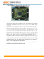
GFEC MAX V Starter Kit
User's Manual
Address: 14F, 207-5, Sec 3, Peihsin Rd.
Hsintien, Taiwan R.O.C.
TEL: 886-2-8913-2200
FAX: 886-2-8913-2277
GALAXY FAR EAST CORP.
Taipei Head Office
14F., No. 207-5, Sec. 2, Bei Hsin Rc., Hsin Dien, New Taipei
TEL: 886-2-8913-2200
FAX: 886-2-8913-2277
Hsinchu Branch
3F., No. 526, Sec. 1, Kuang Fu Rd., Hsinchu City
TEL: 886-3-578-6766
FAX: 886-3-577-4795
Kaohsiung Branch
10F-8, No. 56, Sec. 1, Min Sen 1 Rd., Hsin Hsin District, Kaouhsiung City
TEL: 886-7-223-1338
FAX: 886-7-222-4051
For technical support, please call:
TEL: 0800819595
GALAXY website:
HTTP://WWW.GFEC.COM.TW
2
Table of Contents
Table of Contents ..................................................................... 錯誤! 尚未定義書籤。
Chapter 1
Chapter 2
Appendix A
Appendix B
Instructions.............................................................................................4
Quartus II Starter................................................................................200
Quartus II 10.1 Installation ..................................................................41
Installing Download Cable on Windows XP/Win7 .............................46
3
Chapter 1 Instructions
¾ Contents
z Altera MAX V Main Board
z USB Cable
z CD-ROM
¾ Attention
z Please check the contents of the box are complete when you receive this
Experimental Board.
z The max. voltage of expansion I/O is limited to 3.3V, so that if an IC
(5M1270ZT144C5N) has been burnt out due to carelessness, you will need to
purchase it from our service department and solder it by yourself.
z 3 month warranty is provided for normal use.
¾ Feature
This experimental board is a simulation board specially made for the Altera MAX
V Family of Devices. Those interested in digitizing design could realize their
ideas through this experimental board. The built-in CPLD: 5M1270ZT144C5N
provides 1270 LEs with 114 common I/O, 8K bits User Flash Memory.
Detailed information and specs. are available on the DVD enclosed or on the
Altera Web Site (http://www.altera.com) 。
Except IC: 5M1270ZT144C5N, some peripheral parts connected to it, are
available for users upon completion of a digital logic design.
4
¾ Peripheral parts
4 Bits DIP Switch
2 Push Buttons
8 LEDs
1 Oscillator Socket
4 Extension I/O Connectors
¾ Appearance of MAX V Experimental Board
5
¾ Detailed specs. are listed below:
1. 4 Bits DIP Switch (DIP_SW)
The MAX V Experimental Board comes equipped with a 4-bit DIP Switch; when it is
switched to ON, it will turn MAX V Device I/O on in Low; the signal pin position of
the 4 Bits DIP Switch and the connection to the MAX V Device I/O can be found in
the following table.
Devices
Switch code
DIP1
MAX V pin position
96
4 Bits DIP Switch
DIP2
DIP3
95
94
DIP 4
93
Comments: ON is Low; OFF is High.
2. 2 Push Buttons (SW0 – SW1)
2 Push buttons are available; push button down to direct
the Low signal to the MAX V; leave it without pushing for a High signal. For the
pin positions of the Push Buttons vs. I/O of MAX V Device, please refer to the
following table.
Devices
Push Button code
MAX V pin position
2 Push Buttons
SW0
SW1
108
107
Comments pushed-down: low level; normal: high level.
6
3. 8 LEDs (D1 – D8)
When High signals are sent by MAX V I/O, the LED will light up; the pin positions of
the 8 LEDs vs. I/O of MAX V Device are listed in the following table.
Devices
LED code
MAX V pin position
D1
106
D2
105
D3
104
8 LEDs
D4 D5
103 102
D6
101
D7
98
D8
97
Comments: high level – lit LED; low level -- LED off.
4. Oscillator Socket
A half-long oscillator socket is provided, which can transmit Clock to the MAX V
Device.
The appropriate frequency of the oscillator should be selected by the user when
applying the clock source.
The output of this clock source is connected to the 89 Pin (CLK 2) of MAX V.
7
5. VCC I/O Voltage Selection
4 I/O extension connectors are provided; the VCC I/O in 3 of the connectors is
adjustable.
They are JP5 (IO 2), JP6 (IO 1) andJP7 (IO 4) with their output
voltage ranges at 1.2V, 1.5V, 1.8V, 2.5V and 3.3V. JP4 (IO 3) is a fixed VCC I/O at
3.3V; the user can link to this connector and input a working voltage of 5V for the
experiment board.
VIO1 (JP6):
1: 3.3V
2: 2.5V
3:1.8V
4:1.5V
ALL OFF: 1.2V
VIO2 (JP5):
1: 3.3V
2: 2.5V
3: 1.8V
4: 1.5V
ALL OFF: 1.2V
8
VIO4 (JP7):
1: 3.3V
2: 2.5V
3: 1.8V
4: 1.5V
ALL OFF: 1.2V
6. Power Selection
2 experiment board working voltages are available for selection, which come from the
USB socket or VCC I/O 3(JP4) and which can light up the PWR (D 11) LED.
DC: USB cord
EXT: JP4
9
7. 4 Extension I/O Connectors (JP4 / JP5 / JP6/ JP7)
5M1270ZT144C5N provides 114 common I/O pins. The expansion I/O ports of this
experimental board connect to JP6 (IO 1), JP5 (IO 2), JP4 (IO 3) and JP7 (IO 4),
respectively,
so that the user can easily link this connector to other PC boards. Furthermore, JP6,
JP5 and JP7 also provide the Power Pin and GND pin; Power Pins offer 1.2V, 1.5V,
2.5V and 3.3V voltages but without current protection. We suggest that you set up a
power circuit in your own expansion circuit before connecting the two if a large
current would be obtained from this experimental board. Except for the Power Pin and
GND Pin, other pins of the JP4 to JP7 connectors are directly connected to I/O of
MAX V Device; signals exceeding 3.3V are prohibited to connect to this connector.
Furthermore, besides the partial pins connected to the MAX V Device, some of them
are also connected to other parts on the board (e.g. LED, Push Button etc.), and the
user is advised to pay attention to the possible affect that expansion of the I/O pin
would have on these parts. The mapping of the expansion of the I/O connector vs.
MAX V Device can be found in the following table.
For the JP4, some of the pins are defined as external Asynchronous FIFO, which
enable MAX V to exchange data with other systems.
10
MAX V pin
Connector
position/property
MAX V pin
Connector
position/property
VCC_IO1
JP6 Pin1
VCC_IO2
JP5 Pin1
VCC_IO1
JP6 Pin2
VCC_IO2
JP5 Pin2
GND
JP6 Pin3
144
JP5 Pin3
GND
JP6 Pin4
143
JP5 Pin4
GND
JP6 Pin5
142
JP5 Pin5
GND
JP6 Pin6
141
JP5 Pin6
32
JP6 Pin7
140
JP5 Pin7
31
JP6 Pin8
139
JP5 Pin8
30
JP6 Pin9
138
JP5 Pin9
29
JP6 Pin10
137
JP5 Pin10
28
JP6 Pin11
134
JP5 Pin11
27
JP6 Pin12
133
JP5 Pin12
24
JP6 Pin13
132
JP5 Pin13
23
JP6 Pin14
131
JP5 Pin14
22
JP6 Pin15
130
JP5 Pin15
21
JP6 Pin16
129
JP5 Pin16
16
JP6 Pin17
127
JP5 Pin17
CLK1
JP6 Pin18
125
JP5 Pin18
GND
JP6 Pin19
GND
JP5 Pin19
GND
JP6 Pin20
GND
JP5 Pin20
GND
JP6 Pin21
GND
JP5 Pin21
GND
JP6 Pin22
GND
JP5 Pin22
GND
JP6 Pin23
124
JP5 Pin23
GND
JP6 Pin24
CLK0
JP5 Pin24
14
JP6 Pin25
122
JP5 Pin25
15
JP6 Pin26
123
JP5 Pin26
12
JP6 Pin27
120
JP52 Pin27
13
JP6 Pin28
121
JP5 Pin28
GND
JP6 Pin29
118
JP5 Pin29
GND
JP6 Pin30
119
JP5 Pin30
7
JP6 Pin31
114
JP5 Pin31
8
JP6 Pin32
117
JP5 Pin32
5
JP6 Pin33
112
JP5 Pin33
6
JP6 Pin34
113
JP5 Pin34
3
JP6 Pin35
110
JP5 Pin35
11
4
JP6 Pin36
111
JP5 Pin36
1
JP6 Pin37
GND
JP5 Pin37
2
JP6 Pin38
109
JP5 Pin38
VCC_IO1
JP6 Pin39
VCC_IO2
JP5 Pin39
VCC_IO1
JP6 Pin40
VCC_IO2
JP5 Pin40
MAX V pin
Connector
MAX V pin
Connector
position/property
position/property
Ext_Power
JP4 Pin1
VCC_IO4
JP7 Pin1
Ext_Power
JP4 Pin2
VCC_IO4
JP7 Pin2
LED0/106
JP4 Pin3
GND
JP7 Pin3
LED1/105
JP4 Pin4
72
JP7 Pin4
LED2/104
JP4 Pin5
71
JP7 Pin5
LED3/103
JP4 Pin6
70
JP7 Pin6
LED4/102
JP4 Pin7
69
JP7 Pin7
LED5/101
JP4 Pin8
68
JP7 Pin8
LED6/98
JP4 Pin9
67
JP7 Pin9
LED7/97
JP4 Pin10
66
JP7 Pin10
GND
JP4 Pin11
63
JP7 Pin11
GND
JP4 Pin12
62
JP7 Pin12
DIP0/96
JP4 Pin13
61
JP7 Pin13
DIP1/95
JP4 Pin14
60
JP7 Pin14
DIP2/94
JP4 Pin15
59
JP7 Pin15
DIP3/93
JP4 Pin16
58
JP7 Pin16
SW0/108
JP4 Pin17
57
JP7 Pin17
SW1/107
JP4 Pin18
55
JP7 Pin18
GND
JP4 Pin19
GND
JP7 Pin19
GND
JP4 Pin20
GND
JP7 Pin20
GND
JP4 Pin21
GND
JP7 Pin21
GND
JP4 Pin22
GND
JP7 Pin22
DB0/88
JP4 Pin23
53
JP7 Pin23
DB1/87
JP4 Pin24
CKL3
JP7 Pin24
DB2/86
JP4 Pin25
51
JP7 Pin25
DB3/85
JP4 Pin26
52
JP7 Pin26
DB4/84
JP4 Pin27
49
JP7 Pin27
DB5/81
JP4 Pin28
50
JP7 Pin28
12
GND
JP4 Pin29
45
JP7 Pin29
GND
JP4 Pin30
48
JP7 Pin30
DB6/80
JP4 Pin31
43
JP7 Pin31
DB7/79
JP4 Pin32
44
JP7 Pin32
RxF/75
JP4 Pin33
41
JP7 Pin33
TxF/77
JP4 Pin34
42
JP7 Pin34
RD/74
JP4 Pin35
39
JP7 Pin35
WR/76
JP4 Pin36
40
JP7 Pin36
GPIO/73
JP4 Pin37
37
JP7 Pin37
GND
JP4 Pin38
38
JP7 Pin38
Ext_Power
JP4 Pin39
VCC_IO4
JP7 Pin39
Ext_power
JP4 Pin40
VCC_IO4
JP7 Pin40
8. DC Input Connector
The voltage regulator has been built-in to this experimental board; power can be
obtained by inserting a USB cable into JP16. The LED D11 will light up when the
power comes on.
Users are able to input working power from JP4 (IO3) by switching JP8 to EXT (Pin
1 &2, 39 & 40 of JP4 are for input of EXT_Power).
13
9. JTAG 5X2 Header Connector
The Altera MAX V Device comes with ISP (In System Programming) as a function;
insert the USB Download Cable (sold separately) into the USB port on the PC, with
the other end inserted into JP3. Use Altera’s proprietary software Quartus II and then
download the data onto this experimental board.
14
Circuit diagram of this experimental board
15
16
¾ Easy Download and Installation of Quartus II
A.
Install Altera Quartus II 10.1 SP1 or later by opening the included CD and
clicking
Install Quartus II Web Edition
B.
Apply License
1. Open Quartus II 10.1 (Start => program files => Altera => Quartus II
10.1 )
2. From the main menu, select Tools => License Setup => jot down the
(NIC) ID
3. Then visit http://www.altera.com/support/licensing/lic-index.html, click
Quartus II Web Edition Software License, so you can apply for a free
17
account of Quartus II License.
4. Altera will then return a License.dat file through e-mail. Open Tools
=>License Setup window; via the License file, and place the Lincense.dat
there.
5. When you see the figure as shown on the below, this means that the
installation is complete.
C.
After Compiler is done, select Tools => open Programmer
1. Select Hardware Setup
2. Highlight USB Blaster and click close.
18
D.
E.
Mode => JTAG
Add File,select pof file
F.
If UFM is not in use, check the
following window
Insert the USB Download
cable into JP3
Insert USB into the Power Cable ( JP16)
Press Start to burn.
G.
H.
I.
19
Chapter 2 Quartus II Starter
In this chapter, an example of Marquee in VHDL design shall be revealed and how to
create new projects, program, edit and download, etc. via Quartus II.
It is
necessary to copy the data in the ledtest directory into the hard drive before starting
the following procedure; the example shows how to transfer data from the ledtest to
D:\ledtest\.
Part 1. Create new project
Step 1
Open Project Wizard: 【File】→【New Project Wizard】.
20
Step 2
Click【Next】.
Step 3
Type in project working directory and name, then click【Next】.
21
Step 4
Select ledtest.VHD, click [ADD] and add it into this project; click [Next].
22
Step 5
Select Chip model: 5M1270ZT144C5N of MAX V series.
23
Step 6
Click【Next】.
24
Step 7
Click [Finish] to complete creating the new project.
Part 2. Create program file
The input methods of circuits in Quartus II come with AHDL, Block
Diagram/Schematic, Verilog HDL and VHDL File, etc.; however, an example of
Marquee in VHDL shall be introduced in this chapter. To create a new VHDL
program, click 【File】→【New】to start a designing method; click 【VHDL File】
under 【Design Files】to open a new VHDL programming file. In this example,
programmed codes have been prepared that will only open old files by ledtest.vhd.
25
Step 1.
Open ledtest.vhd.
26
Marquee programming code and description
[Marquee programming code]
LIBRARY ieee;
USE ieee.std_logic_1164.ALL;
USE ieee.std_logic_unsigned.all;
LIBRARY ALTERA;
USE ALTERA.MAXPLUS2.ALL;
ENTITYledtest IS
PORT(
CLK
RESET
: IN
STD_LOGIC;
: IN
STD_LOGIC;
LED_SEL
: IN
STD_LOGIC;
LED
: OUT
STD_LOGIC_VECTOR(7 DOWNTO 0);
DIP_SW
: IN
STD_LOGIC_VECTOR(3 DOWNTO 0)
);
ENDledtest;
ARCHITECTURE a OF ledtest IS
SIGNAL LED_REG
: STD_LOGIC_VECTOR(7 DOWNTO 0);
SIGNAL CNT
: INTEGER RANGE 0 TO 4194303;
SIGNAL CNT_CLK
: STD_LOGIC;
BEGIN
CLK_CNT: PROCESS(CLK,RESET)
BEGIN
IF RESET = '0' THEN
CNT_CLK <= '0';
CNT <= 0;
ELSIF CLK'EVENT AND CLK='1' THEN
IF CNT=4194303 THEN
CNT_CLK <= NOT CNT_CLK;
CNT <= 0;
ELSE
CNT <= CNT + 1;
27
END IF;
END IF;
END PROCESS CLK_CNT;
LED_REG_CON: PROCESS (RESET,CNT_CLK,LED_SEL)
BEGIN
IF RESET='0' THEN
LED_REG <=
"00000001";
ELSIF LED_SEL='0' THEN
LED_REG <= "00000011";
ELSIF CNT_CLK'EVENT AND CNT_CLK='1' THEN
LED_REG(0) <= LED_REG(7);
LED_REG(7 DOWNTO 1) <= LED_REG(6 DOWNTO 0);
END IF;
END PROCESS LED_REG_CON;
LED_OUT: WITH DIP_SW SELECT
LED <= LED_REG
WHEN "1111" ,
"00010001" WHEN "1110" ,
"00100010" WHEN "1101" ,
"01000100" WHEN "1011" ,
"10001000" WHEN "0111" ,
"00000000" WHEN others;
END a;
Step 2
This VHDL file can be constructed as a symbol of an electric circuit for a
circuit diagram Design with the following process:
Step2-1
Open VHDL file to create the symbol, click 【File】→【Create/Update】
→【Create SymbolFiles for Current File】
28
Step 2-2 Complete the symbol to be built
Step 2-3 To create a new Block Diagram, click 【File】→【New】to choose a new
designing method; click 【Block Diagram/Schematic File】under 【Design
Files】to open a new Electric circuit diagram designing file.
29
Step 2-4 Double click on any blank space to open the symbol selection window,
where the ledtest symbol as built under [Project] can be found.
Part 3 Designated chip pin positions
Step 1
Quartus II provides several methods to designate pin positions by selecting
30
one of the them【Assignments】→【Assignment Editor】menu.
Step 2
Double click left <NEW> under the <To> column to open up the Node
Finder as follows:
31
Step 3
Click the selector key on the right of “Look in” in the Node Finder window
and select ledtest; then click list.
All the pin name of the ledtest will be generated in the Node Finder window, select all
of the pins and click OK.
32
Step 4
Left click Assignment Name column and type in Location, repeat until all
Assignment name spaces are filled with Location.
Step 5
Type in the pin positions in the Value column as follows:
33
34
Part 4 Program compilation
Step 1
Compilation : 【Processing】→【Start Compilation】
35
Step 2
Compilation complete
Part 5 Downloading the program
Step 1
Open program 【Tools】→【Programmer】
36
Step 2
Make sure the Download Cable is set; if not, please refer to “Download
Cable” under Windows XP/Win7. If in Hardware Setup, select USB Blaster
[USB-0]; if not, please refer to “Hardware Setup”. Download the file by
selecting ledtest.pof, check all boxes in 【Program/Configure】; at this
moment the MAX V Kit must be connected to the Download Cable and
power cord; finally, click 【Start】to complete downloading.
37
Part 6 Hardware settings and operation descriptions
While DIP SW1 is ON, D0 D4 LED lights up
While DIP SW2 is ON, D1 D5 LED lights up
While DIP SW3 is ON, D2 D6 LED lights up
While DIP SW4 is ON, D3 D7 LED lights up
(Only one DIP SW will be ON at the same time; i.e. if DIP SW1 is ON, all other DIP
SWs shall be OFF, or all LED will not be lit)
When all DIP SWs are OFF, LED shall be in Marquee mode; press SW0 with one
LED lit up; press SW1 to light up two LED.
38
Part 7 Hardware Setup
Step 1
【Tools】→【Programmer】
Step 2
Click【Hardware Setup】
39
Step 3
Select USB Blaster
40
Appendix A Quartus II 10.1 Installation
Step 1
Click【Next】
Step 2
Click [I agree to the terms of the license agreement】, then click【Next】.
41
Step 3
Designate Quartus 10.1 installation path, click [Next].
42
Step 4
Check Quartus,NIOS and Modelsim boxes,then click【Yes】.
43
Step 5
Click【Next】.
Step 6
Start installation.
44
Step 7
Click [Finish] to complete installation.
45
Appendix B Installing Download Cable on Windows XP/ Win7
The download cable is a standard USB hardware interface which requires an
additional driver under XP or Win 7 O/S so that the burning of the chip can go
through the USB interface.
Create new hardware on Windows XP
Step 1
[Start]-> [Setup]-> [Control panel]-> [System]-> [Hardware]-> [Hardware
administrator]-> New hardware wizard pops up --> click [Next]
46
Step 2
Select a directory "From List" or a specific directory for installation -->
click [Next].
Step 3
Select path C:\altera\quartus\drivers\usb-blaster\→ [Next].
47
Step 4
Select [Continue to install] --> [Finish] --> [Next].
Step 5
Installation complete
48
Create new hardware on Windows 7
Step 1
[Start]-> [Setup]-> [Control panel]-> [System]-> [Hardware]-> [Hardware
administrator]-> [New/delete hardware] wizard pops up --> click [Next].
Step 2
Insert Download Cable into USB/PC, select USB-Blaster, right click on it
and select update new driver or software.
49
Step 3
Browse and select the driver from the list --> browse --> select
C:\altera\10.1\quartus\drivers\USB-blaster\ Æ click [Next]
Step 4
Select: Continue to install this driver.
50
Step 5
Installation complete --> [Exit]
Step 6
Installation complete
51
52