1
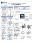
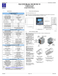
MAN0963-09-EN
XL4 OCS
Datasheet for HE-XC1E0, HE-XC1E2, HE-XC1E3, HE-XC1E4, HE-XC1E5
HEXT251C100, HEXT251C112, HEXT251C113, HEXT251C114, HEXT251C115
1. Specifications
Required Power
(Steady state)
Required Power
(Inrush)
General Specifications
95 mA @ 24 VDC
190 mA @ 12 VDC
2A for <1 ms @ 24 VDC
DC Switched
Primary Power Range
10 – 30 VDC
Relative Humidity
Clock Accuracy
Surrounding Air Temp
Storage Temp
Weight
5 to 95% Non-condensing
+/- 20 ppm maximum at 25° C (+/- 1 min/month)
-10°C to +60°C
-30°C to +70°C
12 oz. (340 g)
Control & Logic Specifications
Advanced Ladder Logic
Full IEC 1131-3 Languages
Control Language Support
1MB, maximum
0.013mS/K
Supported in Advanced Ladder
Logic Program Size
& Logic Scan Rate
Online Programming
Changes
Digital Inputs
2048
Digital Outputs
2048
I/O Support
Analog Inputs
512
Analog Outputs
512
50,000 (words) Retentive
General Purpose Registers
16,384 (bits) Retentive
US Certifications
UL / CE
Europe Certifications
16,384 (bits) Non-retentive
Display Specifications
Connectivity
Serial Ports
1 RS232 & 1 RS485 on single Modular Jack
Display Type
3.5” TFT Transmissive Color
USB mini-B
USB 2.0 (480MHz) Programming & Data Access
Resolution
QVGA (320x240)
USB A
USB 2.0 (480MHz) for USB FLASH Drives (2TB)
Color
16-bit (65,535)
CAN
Remote I/O, Peer-to-Peer Comms, Cscape
Screen Memory
27MB
User-Programmable
10/100 Mb (Auto-MDX)
Ethernet
1023
Screens
Modbus TCP C/S, HTTP, FTP, SMTP, Cscape
Remote I/O
SmartRail, SmartStix, SmartBlock, SmartMod
Backlight
LED – 50,000 hour life
Removable
User Configurable within the scan time.
MicroSD, support for >32GB max.
Screen Update Rate
Memory
(perceived as instantaneous in many cases)
Application Updates, Datalogging, more
Input / Output Specifications
High-Speed Counters
mA/V
mA/V
mA/V
Model
DC In
DC Out
Relays
HS In
HS Out
In
RTD/Tc
Out
Number of Counters
2
Model 2
12
6
4
4
Maximum Frequency
>500kHz each
Model 3
12
12
4
2
2
Accumulator Size
32-bits each
Modes Supported
Model 4
24
16
4
2
2
Model 5
12
12
4
2
2
2
Totalizer
Quadrature
Pulse Meas.
Frequency Meas.
There are 2 high-speed inputs of the total DC Inputs. There are 2 high-speed outputs of the total DC
outputs. Model 2, 3 & 4 feature 12-bit Analog I/O. Model 5 features 14/16-bit Analog I/O. High2 Position Controlled Outputs
speed Outputs can be used for PWM and Pulse Train Outputs, currently limited to <65kHz.
1 ON/OFF Setpoint per Output
2. Dimensions & Panel Cutout
3.622 [92mm]
Panel Cutout
3.622 [92mm]
Cutout tolerance to meet NEMA
standards is ±0.005” (0.1mm).
Max. Panel Thickness is 5mm.
September 20, 2013
Page 1 of 6
MAN0963-09-EN
3. Installation Procedures
1. Carefully locate an appropriate place to mount the XL4. Be sure to leave enough room at the top of the unit for insertion and
removal of the microSD™ card. Also leave enough room at the bottom for the insertion and removal of USB FLASH drives
2. Carefully cut the host panel per the diagram on Page 1, creating a 92mm x 92mm ±0.1mm opening into which the XL4 may be
installed. If the opening is too large, water may leak into the enclosure, potentially damaging the XL4. If the opening is too small,
the OCS may not fit through the hole without damage.
3. Remove all Removable Terminals from the XL4. Insert the XL4 through the panel cutout (from the front). The gasket needs to be
between the host panel and the XL4.
4. Install and tighten the four mounting clips (provided in the box) until the gasket forms a tight seal (max torque 1.5Nm / 13.2Lb-in).
5. Reinstall the XL4 I/O Removable Terminal Blocks. Connect communications cables to the serial port, USB ports, Ethernet port,
and CAN port as required.
4. Ports & Connectors
XL4 Connector Locations
September 20, 2013
Page 2 of 6
MAN0963-09-EN
DC Input / Frame
CAN
Torque rating
4.5 – 7 Lb-In
(0.50 – 0.78 N-m)
Locking Spring-Clamp,
Two-terminators Per Conductor
Torque rating 4.5 Lb-In
(0.50 N-m)
DC- is internally connected to
I/O V-, but is isolated from
CAN VA Class 2 power supply must
be used.
SHLD and V+ pins are not
internally connected to XL4
MJ1/2 Serial Ports
DIP Switches
MJ1: RS-232 w/Full
Handshaking
1 2 3
MJ2: RS-485 Half-Duplex
Two Serial Ports on One Modular Jack (8posn)
Pin
8
7
6
5
4
3
2
1
MJ1 Pins
ON
MJ2 Pins
Signal
Direction
Signal
Direction
TXD
OUT
-
-
RXD
0V
IN
Ground
0V
Ground
+5V@60mA
RTS
OUT
OUT
+5V@60mA
-
OUT
-
CTS
-
IN
-
RX- / TXRX+ / TX+
IN / OUT
IN / OUT
Pin
Name
Function
Default
1
RS-485 Termination
ON = Terminated
OFF
2
3
Spare
Factory Use
Always Off
Always Off
OFF
OFF
5. Safety
WARNING: Only qualified electrical personnel familiar with the construction and operation of this equipment and the hazards involved should
install, adjust, operate, or service this equipment. Read and understand this manual and other applicable manuals in their entirety before
proceeding. Failure to observe this precaution could result in severe bodily injury or loss of life.
WARNING: To avoid the risk of electric shock or burns, always connect the earth ground before making any other connections.
WARNING: To reduce the risk of fire, electrical shock, or physical injury it is strongly recommended to fuse all Power Sources connected to
the OCS. Be sure to locate fuses as close to the source as possible.
WARNING: Replace fuse with the same type and rating to provide protection against risk of fire and shock hazards.
WARNING: In the event of repeated failure, do not replace the fuse again as a repeated failure indicates a defective condition that will not
clear by replacing the fuse.
WARNING: Battery may explode if mistreated. Do Not Recharge, Disassemble or Dispose Of in Fire.
WARNING: EXPLOSION HAZARD – BATTERIES MUST ONLY BE CHANGED IN AN AREA KNOWN TO BE NON-HAZARDOUS
Power input and output (I/O) wiring must be in accordance with Class I, Division 2 wiring methods of the National Electric Code, NFPA 70 for
installations in the U.S., or as specified in Section 18-1J2 of the Canadian Electrical Code for installations within Canada and in accordance
with the authority having jurisdiction. This equipment is suitable for use in Class I, Division 2, Groups A, B, C, and D or Non-hazardous
locations only.
WARNING: EXPLOSION HAZARD – Do not disconnect equipment unless power has been switched off or the area is known to be nonhazardous.
WARNING: EXPLOSION HAZARD – Substitution of components may impair suitability for Class 1, Division 2. Digital outputs shall be
supplied from the same source as the Operator Control Station. Jumpers on connector JP1 and others shall not be removed or replaced while
the circuit is live unless the area is known to be free of ignitable concentrations of flammable gasses or vapors.
6. Technical Support
For assistance and manual
updates, contact Technical
Support at the following
locations:
North America
(317) 916-4274
877-665-5666
http://www.heapg.com
e-mail: [email protected]
Europe
(+) 353-21-4321-266
http://www.horner-apg.com
e-mail: [email protected]
7. Common Cause of Analog Input Tranzorb Failure
A common cause of Analog Input Tranzorb Failure on Analog Inputs Model 2, 3, 4 & 5:
If a 4-20mA circuit is initially wired with loop power, but without a load, the Analog input
could see 24Vdc. This is higher than the rating of the tranzorb. This can be solved by
NOT connecting loop power prior to load connection, or by installing a low-cost PTC in
series between the load and Analog input. See SUP0977-01 for additional details.
NOTE†: Refers to Model 2 – orange (pg.4) Models 3 & 4 – J1 (pg.5) and
Model 5 – 20mA Analog In (pg.6.)
September 20, 2013
Page 3 of 6
MAN0963-09-EN
8. Built-in I/O (Model 2, 3, 4 & 5)
All XL4 models (except the HE-XCE0) feature built-in I/O. The I/O is mapped into OCS Register space, in three separate areas –
Digital/Analog I/O, High-Speed Counter I/O, and High-speed Output I/O. Digital/Analog I/O location is fixed starting at 1, but the High-speed
Counter and High-speed Output references may be mapped to any open register location. For more details on using the High-Speed
Counter and High-Speed Outputs, see the XL4 OCS User’s Manual (MAN0964).
Fixed
Address
XL4 Model
Digital/Analog
I/O Function
3
4
1-12
1-12
1-24
1-12
%I1601
Reserved
13-32
13-31
25-31
ESCP Alarm
n/a
32
32
Digital Outputs
1-6
1-12
1-16
Reserved
7-24
13-24
17-24
Analog Inputs
1-4
1-2
1-2
Reserved
5-12
3-12
3-12
Reserved
n/a
1-8
1-8
Analog Outputs
n/a
n/a
n/a
Reserved areas maintain backward compatibility
with other XL Series OCS models
13-31
32
1-12
13-24
1-2
3-12
1-8
9-10
%Q1601
%AI0401
Digital Inputs
%I1
%Q1
%AI1
%AQ1
Default
Address*
2
5
High-Speed Counter
Function
XL4 Models
2-5
Default
Address*
1-8
%I1617
Status Bits
Command Bits
1-32
Accumulator 1 & 2
1-8
Preload & Match
%AQ0401
1-12
Values
*Starting Address locations for %I, %Q, %AI & %AQ may
be re-mapped by user
High-Speed Output
Function
Status Bits
XL4 Models
2-5
1-8
%Q1**
n/a
Command Bits
1-2
n/a
n/a
PWM or Pulse-Train
%AQ421
1-20
Parameters
*Starting Address locations for %I & %AQ may be
remapped by user
**Q1-Q2 are part of the Fixed I/O Map. In High-Speed
Output mode they can be used to initiate a Stepper/PTO
Move
Model 2 I/O
The XL4 model 2 (HE-XC1E2) features 12 DC Inputs, 6 Relay outputs, and 4 Analog Inputs. The DC Inputs are 12/24Vdc compatible, and
can be jumpered for Positive Logic (sinking), or Negative Logic (sourcing). Four of the inputs (H1-H4) can be used for high-speed functions
up to 500kHz. The 12-bit Analog Inputs can be jumpered for voltage (0-10V) or current (4-20mA) on a channel by channel basis. The
Relay outputs are isolated, supporting AC and DC voltages, with output currents of up to 3A/relay, 5A total.
Orange
Digital In / Analog In
J1
(Orange)
I1
I2
I3
I4
I5
I6
I7
I8
H1
0V
A1
A2
A3
A4
0V
Black
Relay Out / Digital In
J2
(Black)
C6
R6
C5
R5
C4
R4
C3
R3
C2
R2
C1
R1
H4
H3
H2
I1
I2
Name
IN1
IN2
IN3
IN4
IN5
IN6
IN7
IN8
HSC1 / N9
Common
Analog IN1
Analog IN2
Analog IN3
Analog IN4
Common
I3
I4
I5
12-24VDC
I6
I7
I8
H1
0V
20mA
A1
A2
A3
LOOP PWR
Name
Relay 6 COM
Relay 6 NO
Relay 5 COM
Relay 5 NO
Relay 4 COM
Relay 4 NO
Relay 3 COM
Relay 3 NO
Relay 2 COM
Relay 2 NO
Relay 1 COM
Relay 1 NO
HSC4 / IN12
HSC3 / IN11
HSC2 / IN10
A4
0-10VDC
230VAC
OR
25VDC
230VAC
OR
25VDC
230VAC
OR
25VDC
230VAC
OR
25VDC
230VAC
OR
25VDC
230VAC
OR
25VDC
0V
12-24VDC
0V ON J1
J2
JP2
Location of I/O jumpers
(JP1 & JP2) and
wiring connectors
(J1 and J2) with back cover
removed.
C5
N
L
LOAD
LOAD
LOAD
LOAD
R2
C1
N
L
R3
C2
N
L
R4
C3
N
L
R5
C4
N
L
R6
LOAD
R1
H3
H2
JP2 Analog In (A1 – A4)
Current
Voltage
(20 mA)
(10 V)
A1
A2
A3
A4
JP1
001XLE025
LOAD
001XLE015
Model 2 Jumper Setting Details
J1
L
H4
001XLE017
JP1 Digital DC In / HSC
Positive Negative
Logic
Logic
C6
N
Default
001XLE026
Default
001XLE027
Note: The Cscape Module Setup configuration must match the
selected I/O (JP) jumper settings.
Note: When using JP2 (A1-A4), each channel can be
independently configured.
"WARNING: EXPOSURE TO SOME CHEMICALS MAY DEGRADE
THE SEALING PROPERTIES OF MATERIALS USED IN THE Tyco relay PCJ
Cover / case & base: Mitsubishi engineering Plastics Corp.
5010GN6-30 or 5010GN6-30 M8 (PBT)
Sealing Material: Kishimoto 4616-50K (I part epoxy resin)
It is recommended to periodically inspect the relay for any
degradation of properties and replace if degradation is found
September 20, 2013
Page 4 of 6
MAN0963-09-EN
Model 3 & Model 4 I/O
The XL4 model 3 (HE-XC1E3) features 12 DC Inputs, 12 DC outputs, and 2 Analog Inputs. The XL4 model 4 (HE-XC1E4) increases the I/O
count up to 24 DC Inputs, and 16 DC Outputs and 2 Analog Inputs. The DC Inputs are 12/24Vdc compatible, and can be jumpered for
Positive Logic (sinking), or Negative Logic (sourcing). Four of the inputs (H1-H4) can be used for high-speed functions up to 500kHz. The
12-bit Analog Inputs can be jumpered for voltage (0-10V) or current (4-20mA) on a channel by channel basis. The 12/24VDC Outputs
feature Electronic Short Circuit protection, and support currents up to 0.5A per point, and 4A total. Two of the DC Outputs can be used for
high speed functions (PWM or PTO). The output frequency is limited by the switching capability of the output drivers (about 10kHz),
although an optional accessory (HE-XHSQ) can be added to provide parallel output drivers supporting frequencies up to 200kHz.
J1 Orange
Positive Logic
Digital & Analog In
J1
(Orange)
I1
I2
I3
I4
I5
I6
I7
I8
H1
H2
H3
H4
A1
A2
0V
Model 3 & 4
Signal Name
IN1
IN2
IN3
IN4
IN5
IN6
IN7
IN8
HSC1 / IN9
HSC2 / IN10
HSC3 / IN11
HSC4 / IN12
Analog IN1
Analog IN2
Common
J3
(Orange)
I13
I14
I15
I16
I17
I18
I19
I20
I21
I22
I23
I24
0V
J2 Black
Positive Logic
Digital Out
Jumper Setting Details
Model 3
Model 4
Name
Name
Common
V+ *
No
NC
OUT13
Connect
Q12
OUT12
Q11
OUT11
Q10
OUT10
Q9
OUT9
Q8
OUT8
Q7
OUT7
Q6
OUT6
Q5
OUT5
Q4
OUT4
Q3
OUT3
Q2
OUT2 / PWM2
Q1
OUT1 / PWM1
*V+ Supply for Sourcing Outputs
J1
JP3
J3
J2
JP3 Analog Inputs
001XLE005-R1
Location of I/O jumpers
(JP1 & JP3) and
wiring connectors
(J1, J2, J3 & J4) with back
cover removed.
Note: The Cscape Module Setup configuration
must match the selected I/O (JP) jumper
settings.
Note: When using JP3 (A1-A2), each channel
can be independently configured.
10 - 30VDC
0V
V+
Model 4
Name
September 20, 2013
Negative Logic
Default
J2
OUT16
OUT15
OUT14
JP1 Digital DC Inputs
JP1
J4 Orange
Positive Logic
Digital Out
Q16
Q15
Q14
J3 Orange
Positive Logic
Digital In
Positive Logic
J4
J2
(Black)
0V
V+
J4
(Orange)
Model 4 only
Signal Name
IN13
IN14
IN15
IN16
IN17
IN18
IN19
IN20
IN21
IN22
IN23
IN24
Common
J4
LOAD
Q16
LOAD
Q15
LOAD
Q14
Note:
Model 3 uses
J1 & and J2 only.
Model 4 uses
J1, J2, J3 & J4.
Page 5 of 6
MAN0963-09-EN
Model 5 I/O
The XL4 model 5 (HE-XC1E5) features 12 DC Inputs, 12 DC outputs, with high performance, highly configurable Analog Inputs (2) and
Analog Outputs (2). , The DC Inputs are 12/24Vdc compatible, and can be jumpered for Positive Logic (sinking), or Negative Logic
(sourcing). Four of the inputs (H1-H4) can be used for high-speed functions up to 500kHz. The 12/24VDC Outputs feature Electronic Short
Circuit protection, and support currents up to 0.5A per point, and 4A total. Two of the DC Outputs can be used for high speed functions
(PWM or PTO). The output frequency is limited by the switching capability of the output drivers (about 10kHz), although an optional
accessory (HE-XHSQ) can be added to provide parallel output drivers supporting frequencies up to 200kHz.
The two high resolution Analog Inputs can be configured for 4-20mA, 0-10V, or 0-100mV at 14-bit resolution. They also can be configured
for 16-bit temperature measurement – supporting Thermocouples or RTDs with 0.05°C resolution. The Analog Outputs are sourcing, and
can be configured for 4-20mA or 0-10V at 14-bit resolution. Each Analog Input or Output channel can be configured independently for
maximum flexibility.
J2 Black
Positive Logic
Digital Outputs
J1 Orange
Positive Logic
Digital Inputs
J1
(Orange)
I1
I2
I3
I4
I5
I6
I7
I8
H1
H2
H3
H4
NC
NC
0V
0V
J2
(Black)
0V
V+*
NC
Q12
Q11
Q10
Q9
Q8
Q7
Q6
Q5
Q4
Q3
Q2
Q1
Name
IN1
IN2
IN3
IN4
IN5
IN6
IN7
IN8
HSC1 / IN9
HSC2 / IN10
HSC3 / IN11
HSC4 / IN12
No Connect
No Connect
Common
Name
V+
10 - 30VDC
Common
Output Power
No Connect
OUT12
OUT11
OUT10
OUT9
OUT8
OUT7
OUT6
OUT5
OUT4
OUT3
OUT2 / PWM2
OUT1 / PWM1
NC
Q12
LOAD
LOAD
Q11
LOAD
Q10
LOAD
Q9
LOAD
Q8
LOAD
Q7
LOAD
Q6
LOAD
Q5
LOAD
Q4
LOAD
Q3
LOAD
Q2
Q1
LOAD
001XLE008
J3
(Orange)
T1+
T1T2+
T2AQ1
AQ2
0V
MA1
V1
0V
MA2
V2
0V
Name
0 – 10 V Analog In
Tc (1 +) or RTD (1+) or
100mV (1+)
Tc (1-) or RTD (1-) or
100mV (1-)
Tc (2+) or RTD (2+) or
100mV (2+)
Tc (2-) or RTD (2-) or
100mV (2-)
10V or 20mA Out (1)
10V or 20mA Out (2)
Common
0-20mA In (1)
0-10V In (1)
Common
0-20mA In (2)
0-10V In (2)
Common
JP1
JP2
NC
MA1
Thermocouple In
mV In
4 - 20 mA Analog Out
100mV+
T1+
100mV-
T1-
V1
0V
0V
0V
RTD In
20 mA Analog In
20mA
MA1
V1
LOOP PWR
0 -10 V Analog Out
T1+
Note: Be sure to wire 0 V
to V1 as shown for proper
operation.
0V
Note:
Loop Power requirements are determined by the transmitter specification.
10VDC
T1-
AQ1
0V
0V
JP2 & JP3
ANALOG INPUT SETTING
RTD (PT100)
T/C/100mV
JP3
JP2
JP3
JP2
JP3
T1
T2
T1
T2
J2
JP4
ANALOG OUTPUT SETTING
VOLTAGE OR CURRENT
CURRENT
(20mA)
JP4
JP1 Digital DC Inputs
Positive Logic
VOLTAGE
(10V)
10V/20mA
Negative Logic
JP2
J3
AQ1
T1-
0-10VDC
Jumper Setting Details
J1
20mA
T1+
JP3
AQ2
AQ1
AQ2
AQ1
001XLE030
Location of I/O jumpers (JP1-JP4) and
wiring connectors (J1-J4)
with back cover removed.
September 20, 2013
Default
Default
MA1/V1
MA2/V2
Default
Page 6 of 6