1
85
Vol 03, Issue 01; January-April 2012
http://technicaljournals.org
International Journal of VLSI and Embedded Systems-IJVES
ISSN: 2249 – 6556
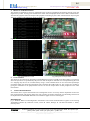
Fig 1. UART communication as reciever.
As a Transmitter
The UART Transmitter is composed of three basic parts.
1) A parallel-load shift register,
2) A transmission line flip-flop, and
3) Logic that generates a “register-empty” flag.
Data is loaded in parallel fashion into the shift register, and then shifted out serially to the Line flip-flop, which
holds the transmitted data for one clock cycle. Remember you must also append the Start and Stop bits to the
data in the shift register. As a bit leaves the shift register, 0‟s are shifted into the “empty” slots of the shiftregister. The flag logic should detect when the shift register has all zeros (i.e. the Stop bits have left the shift
register), and set a flag that the transmission is complete. Upon completion of a successful transmission, the
shift register should then load in the next byte of data.
3. EXPERIMENTAL SET UP
In this paper the authors had implemented the experimental set up on Diligent Nexys2 board, which consider of
the required peripherals for the evaluation of the paper. The detail explanation of each peripheral is as follows.
Seven segment display
The Nexys2 board contains a four-digit common anode seven-segment LED display. Each of the four digits is
composed of seven segments arranged in a “figure 8” pattern, with an LED embedded in each segment. Segment
LEDs can be individually illuminated, so any one of 128 patterns can be displayed on a digit by illuminating
certain LED segments and leaving the others dark. Of these 128 possible patterns, the ten corresponding to the
decimal digits are the most useful. The anodes of the seven LEDs forming each digit are tied together into one
“common anode” circuit node, but the LED cathodes remain separate. The common anode signals are available
as four “digit enable” input signals to the 4-digit display.
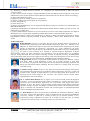
Fig 2. Digilent nexys2 Seven segment Display.
A scanning display controller circuit can be used to show a four-digit number on this display. This circuit drives
the anode signals and corresponding cathode patterns of each digit in a repeating, continuous succession, at an
update rate that is faster than the human eye can detect.
LED`s
The Nexys2 board includes several input devices, output devices, and data ports, allowing many designs to be
implemented without the need for any other components. Eight LEDs are provided for circuit outputs. LED
anodes are driven from the FPGA via 390-ohm resistors, so a logic „1‟ output will illuminate them with 3-4ma
of drive current. A ninth LED is provided as a power-on LED, and a tenth LED indicates FPGA programming
status.
Push Buttons
Four pushbuttons and eight slide switches are provided for circuit inputs. Pushbutton inputs are normally low,
and they are driven high only when the pushbutton is pressed. Slide switches generate constant high or low
inputs depending on their position. Pushbutton and slide switch inputs use a series resistor for protection against
short circuits and a short circuit would occur if an FPGA pin assigned to a pushbutton or slide switch was
inadvertently defined as an output.
Fig 3. Diligent Nexys2 I/O devices.
2011 - TECHNICALJOURNALS®, Peer Reviewed International Journals-IJCEA, IJESR, RJCSE, PAPER, ERL, IRJMWC, IRJSP,
IJEEAR, IJCEAR, IJMEAR, ICEAR, IJVES, IJGET, IJBEST – TJ-PBPC, India;
Indexing in Process - EMBASE, EmCARE, Electronics & Communication Abstracts, SCIRUS, SPARC, GOOGLE Database, EBSCO, NewJour, Worldcat,
DOAJ, and other major databases etc.,