1
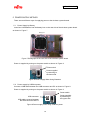
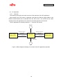
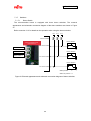
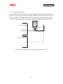
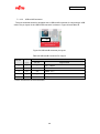
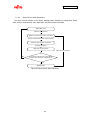
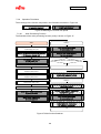
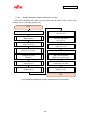
The following document contains information on Cypress products. AN706-00038-2v0-E 32-BIT MICROCONTROLLER FM3 family Application Note Wireless System Board User Manual ARM and Cortex-M3 are the trademarks of ARM Limited in the EU and other countries. AN706-00038-2v0-E All Rights Reserved. The contents of this document are subject to change without notice. Customers are advised to consult with FUJITSU sales representatives before ordering. The information, such as descriptions of function and application circuit examples, in this document are presented solely for the purpose of reference to show examples of operations and uses of Fujitsu semiconductor device; Fujitsu does not warrant proper operation of the device with respect to use based on such information. When you develop equipment incorporating the device based on such information, you must assume any responsibility arising out of such use of the information. Fujitsu assumes no liability for any damages whatsoever arising out of the use of the information. Any information in this document, including descriptions of function and schematic diagrams, shall not be construed as license of the use or exercise of any intellectual property right, such as patent right or copyright, or any other right of Fujitsu or any third party or does Fujitsu warrant non-infringement of any third-party’s intellectual property right or other right by using such information. Fujitsu assumes no liability for any infringement of the intellectual property rights or other rights of third parties which would result from the use of information contained herein. The products described in this document are designed, developed and manufactured as contemplated for general use, including without limitation, ordinary industrial use, general office use, personal use, and household use, but are not designed, developed and manufactured as contemplated (1) for use accompanying fatal risks or dangers that, unless extremely high safety is secured, could have a serious effect to the public, and could lead directly to death, personal injury, severe physical damage or other loss (i.e., nuclear reaction control in nuclear facility, aircraft flight control, air traffic control, mass transport control, medical life support system, missile launch control in weapon system), or (2) for use requiring extremely high reliability (i.e., submersible repeater and artificial satellite). Please note that Fujitsu will not be liable against you and/or any third party for any claims or damages arising in connection with above-mentioned uses of the products. Any semiconductor devices have an inherent chance of failure. You must protect against injury, damage or loss from such failures by incorporating safety design measures into your facility and equipment such as redundancy, fire protection, and prevention of over-current levels and other abnormal operating conditions. If any products described in this document represent goods or technologies subject to certain restrictions on export under the Foreign Exchange and Foreign Trade Law of Japan, the prior authorization by Japanese government will be required for export of those products from Japan. The company names and brand names herein are the trademarks or registered trademarks of their respective owners. Copyright© 2011-2012 FUJITSU SEMICONDUCTOR LIMITED all rights reserved 1 AN706-00038-2v0-E Revision History Rev Date Remark 1.0 Aug.24,2011 First Edition 2.0 Feb.6,2012 Updated to latest format Deleted about FW and GUI part 2 AN706-00038-2v0-E Table of Contents Revision History .......................................................................................................................2 Table of Contents .....................................................................................................................3 Target products ........................................................................................................................6 1 INTRODUCTION ..............................................................................................................7 2 NOTES .............................................................................................................................7 3 OVERVIEW OF THE WIRELESS SYSTEM BOARD ......................................................8 4 PREPARING THE DEVICE ..............................................................................................9 5 6 4.1 Items Included with the Product ................................................................................9 4.2 Required Equipment Not Included with the Product .............................................. 10 4.3 External Appearance of the Wireless System Board .............................................. 11 4.4 Connecting the RS232C Communication Conversion Cable ................................ 12 4.5 Setting up the PC ................................................................................................... 13 POWER SUPPLY METHOD ......................................................................................... 14 5.1 Power Supply by Battery........................................................................................ 14 5.2 Power supply by USB bus power .......................................................................... 14 OPERATIONS ............................................................................................................... 15 6.1 Wireless System Board Operations ....................................................................... 15 6.1.1 6.1.1.1 CPU Operation Modes ............................................................................ 15 6.1.1.2 Overview of Operating the Application .................................................... 16 6.1.2 6.2 7 Overview ......................................................................................................... 15 Operation ........................................................................................................ 18 PC Operation ......................................................................................................... 19 6.2.1 Overview ......................................................................................................... 19 6.2.2 Operation ........................................................................................................ 20 6.2.2.1 Setting the Port Number .......................................................................... 20 6.2.2.2 TOP Screen ............................................................................................. 20 6.2.2.3 Sensor Logger Mode Screen .................................................................. 21 6.2.2.4 Remote Control Mode Screen ................................................................. 22 SPECIFICATIONS......................................................................................................... 23 7.1 Hardware................................................................................................................ 23 7.1.1 General Specifications .................................................................................... 23 7.1.2 Wireless Specifications ................................................................................... 24 7.1.3 Hardware Block Diagram ................................................................................ 25 7.1.4 Main Components ........................................................................................... 26 3 AN706-00038-2v0-E 7.1.5 Microcontroller ................................................................................................ 28 7.1.6 Sensors ........................................................................................................... 33 7.1.7 Switches.......................................................................................................... 35 7.1.7.1 Demo Switch ........................................................................................... 35 7.1.7.2 Reset Switch............................................................................................ 36 7.1.7.3 Microcontroller Mode Selection Switch ................................................... 37 7.1.7.4 Power Switch ........................................................................................... 37 7.1.8 Display Device Specifications ......................................................................... 38 7.1.8.1 Power LED .............................................................................................. 38 7.1.8.2 Demo LED ............................................................................................... 39 7.1.8.3 LCD.......................................................................................................... 40 7.1.9 Real Time Clock.............................................................................................. 41 7.1.10 Voltage Monitor IC .......................................................................................... 42 7.1.11 Power Supply Jumper .................................................................................... 43 7.1.12 Interface Specifications ................................................................................... 44 7.2 7.1.12.1 Board Connection Connector .................................................................. 44 7.1.12.2 User Connector ....................................................................................... 47 7.1.12.3 USB miniB Connector ............................................................................. 49 7.1.12.4 RS232C Connector ................................................................................. 50 7.1.12.5 ICE Connector ......................................................................................... 51 Software ................................................................................................................. 52 7.2.1 Software Block Diagram ................................................................................. 52 7.2.2 System Specifications ..................................................................................... 53 7.2.2.1 Microcontroller System Specifications .................................................... 53 7.2.2.2 Memory Map............................................................................................ 54 7.2.2.3 MFS System Specifications ..................................................................... 55 7.2.2.4 Interrupt System Specifications ............................................................... 55 7.2.3 Operating Conditions ...................................................................................... 57 7.2.4 Overall Application Operating Flow ................................................................ 57 7.2.4.1 Operation From Startup to Demo Mode Selected ................................... 57 7.2.4.2 Operation of Host Device in Sensor Logger Mode and Remote Control Mode 58 7.2.4.3 Operation of Slave Devices in Sensor Logger Mode .............................. 59 7.2.4.4 Operation of Slave Devices in Remote Control Mode ............................ 61 7.2.5 Application State Transitions .......................................................................... 62 7.2.5.1 State Transitions from Startup to Standby State ...................................... 62 4 AN706-00038-2v0-E 7.2.5.2 Host Device State Transitions ................................................................. 62 7.2.5.3 Slave Device State Transitions ................................................................ 63 7.2.6 Relationship Between Demo Modes and CPU Operation Modes in Each Application State............................................................................................................ 64 7.2.7 Application States ........................................................................................... 65 7.2.8 Operation Flowcharts...................................................................................... 68 7.2.8.1 Main Processing Function ....................................................................... 68 7.2.8.2 Sample Application System Initialization Function .................................. 69 7.2.8.3 Demo Operation Mode Decision Function .............................................. 70 7.2.8.4 Sample Application Demo Operation Function ....................................... 71 7.2.8.5 Sensor Measurement Value Read and Sensor Measurement Value Wireless Send Function ............................................................................................. 74 7.2.8.6 Sensor Measurement Value Wireless Send Function ............................ 75 7.2.8.7 Data Wireless Receive Notification Function .......................................... 76 7.2.8.8 Data Wireless Send Complete Notification Function .............................. 77 7.2.8.9 Periodic Processing Function .................................................................. 78 7.2.8.10 Battery Status Monitoring Function ......................................................... 79 5 AN706-00038-2v0-E Target products This application note is described about below products; (TYPE0) Series Product Number (not included Package suffix) MB9B500B MB9BF504NB,MB9BF505NB,MB9BF506NB MB9BF504RB,MB9BF505RB,MB9BF506RB MB9B400B MB9BF404NB,MB9BF405NB,MB9BF406NB MB9BF404RB,MB9BF405RB,MB9BF406RB MB9B300B MB9BF304NB,MB9BF305NB,MB9BF306NB MB9BF304RB,MB9BF305RB,MB9BF306RB MB9B100B MB9BF102NB,MB9BF104NB,MB9BF105NB,MB9BF106NB MB9BF102RB,MB9BF104RB,MB9BF105RB,MB9BF106RB 6 AN706-00038-2v0-E 1 INTRODUCTION This user manual describes how to use and the specifications of the wireless system board. 2 NOTES The hardware used in this wireless system board and the software that controls the microcontroller have been certified as compliant with the technical standards in the Radio Law of Japan. If you make any modifications or changes to the hardware or software in the system, you should check the law and take the appropriate measures to ensure that you do not infringe the Radio Law of Japan. Furthermore, all of the countries around the world have established various rules and regulations regarding safety, electromagnetic interference, and radio waves. You should comply with these rules and regulations when using or designing this wireless system board. Please understand that Fujitsu will bear absolutely no liability for any damages arising from the use of this wireless system board. 7 AN706-00038-2v0-E 3 OVERVIEW OF THE WIRELESS SYSTEM BOARD The wireless system board has two demo operation modes as follows. ① Sensor Logger Mode The slave devices read the measurement values from the hygro-thermometer and illumination sensor and send them to the host device by wireless communication. Communication is possible with up to 4 slave devices for each host device. (Communication is possible with up to a maximum of 15 devices by expanding the system) The host device sends the data received from the slave devices to a PC via UART. ② Remote Control Mode The slave devices read the measurement value of the accelerometer at an interval of 200 milliseconds, and send the value to the host device by wireless communication. Communication is between one slave device for each host device. The host device sends the data received from the slave device to a PC via UART. Built-in LCD and Sensor Sensor control Slave 1 Slave 2 950MHz LCD control Wireless communication Sensor measurement value display Host RS232C communication Slave 3 Figure 1 System overview diagram 8 AN706-00038-2v0-E 4 PREPARING THE DEVICE 4.1 Items Included with the Product A list of the items included with the wireless system board is shown in Table 1, a photograph of the external appearance of the host and slave wireless system boards is shown in Figure 2, and a photograph of the external appearance of the RS232C communication conversion cable is shown in Figure 3. Table 1 List of Items in the Package No Name Qty. Remarks . 1 Host wireless system board 1 The hardware is the same as No.2 2 Slave wireless system board 1 The hardware is the same as No.1 3 RS232C communication conversion cable RS232C cable that connects between No.1 1 and the PC Figure 2 Host and slave wireless system boards Figure 3 RS232C communication conversion cable 9 AN706-00038-2v0-E 4.2 Required Equipment Not Included with the Product A list of required equipment that is not included with the product is shown in Table 2, and a list of equipment that can be used if needed is shown in Table 3. Table 2 List of Required Equipment Not Included with the Product No Name Qty. Remarks . 1 2 3 PC 1 Application 1 executable file RS232C cable 1 Power supply device 4 Application software that runs on the PC Can be downloaded from the WEB Cross cable Select depending on the power supply method (1) AAA battery 4 Used when power supplied by battery (2) USB cable 1 Cable with TypeA-miniB connector Table 3 List of Equipment to be used if needed No. 1 Name ICE Qty. 1 Remarks Required when performing software debugging 10 AN706-00038-2v0-E 4.3 External Appearance of the Wireless System Board Photographs of the external appearance of the host and slave wireless system boards are shown in Figure 4 and Figure 5. Microcontroller board Wireless board USB connector LED2 LED1 Accelerometer Power switch Power LED Wireless transceiver ICE connection connector Demo switch 1 Demo switch 2 Demo switch 3 LCD User connector Board connection connector Microcontroller Pattern antenna (MB9BF506R) RS232C connector Illumination sensor Hygro-thermometer Figure 4 External appearance of the wireless system boards (front surface) 11 AN706-00038-2v0-E Reset switch Mode switch Real time clock AAA battery box Button battery and battery box Figure 5 External appearance of the wireless system boards (rear surface) 4.4 Connecting the RS232C Communication Conversion Cable A diagram inserting the RS232C communication conversion cable that is used for connection the host wireless system board to a PC is shown in Figure 6. Insert Figure 6 Connecting the wireless system board and RS232C communication conversion cable 12 AN706-00038-2v0-E 4.5 Setting up the PC GUI is used for demonstration. In this chapter, the explanation of GUI is omitted. 13 AN706-00038-2v0-E 5 POWER SUPPLY METHOD There are two different ways of supplying power to the wireless system boards. 5.1 Power Supply by Battery Insert four AAA batteries into the battery box on the rear side of the wireless system board as shown in Figure 7. Battery box Figure 7 Photograph of the rear side of the wireless system board Power is supplied by turning on the power switch as shown in Figure 8. 電源スイッチ Power switch ↓側に入れることで Power supplied 電源供給 by switching to the lower side Figure 8 Power Supply When Using Batteries 5.2 Power supply by USB bus power Connect a USB cable between the USB connector and PC as shown in Figure 9. Power is supplied by turning on the power switch as shown in Figure 9. Power switch 電源スイッチ ↑側に入れることで Power supplied 電源供給 by switching to USBコネクタ USB connector USBコネクタとPC間に USB cable connects between USBケーブルを接続 the USB connector and PC the upper side Figure 9 Power supply when using USB bus power 14 AN706-00038-2v0-E 6 OPERATIONS 6.1 Wireless System Board Operations 6.1.1 Overview 6.1.1.1 CPU Operation Modes The wireless system boards have three CPU operation modes as shown in Table 4. Host devices have mode 1 and mode 2, and slave devices have mode 1, mode 2, and mode 3. Table 4 CPU Operation Modes CPU operation Microcontroller operation state mode 1 CPU regular operation (PLL oscillator) Host Slave devices devices ○ ○ ○ ○ - ○ CPU CLK=80MHz Peripheral CLK=40MHz 2 CPU regular operation (PLL oscillator) CPU CLK=60MHz Peripheral CLK=30MHz 3 CPU intermittent operation oscillator/CR oscillator) When active: PLL oscillator CPU CLK=80MHz Peripheral CLK=40MHz When standby: CR oscillator CPU CLK=Stopped Peripheral CLK=4MHz 15 (PLL AN706-00038-2v0-E 6.1.1.2 Overview of Operating the Application A block diagram showing an overview of the operation of the wireless system board application is shown in Figure 10. At startup, you can choose between “Sensor Logger Mode” and “Remote Control Mode”, and in “Sensor Logger Mode”, you can also choose the CPU operation mode while running. Startup ① Was Demo switch1 pressed? No Yes "Remote Control Mode" selected "Sensor Logger Mode" selected Sensor, RF, etc. processing Sensor, RF, etc. processing ② No Was Demo switch1 pressed? Yes Is Host? No Yes Change CPU operation mode Change CPU operation mode 1 CPU=80MHz,Peripheral=40MHz 2 CPU=60MHz,Peripheral=30MHz 1 CPU=80MHz,Peripheral=40MHz 2 CPU=60MHz,Peripheral=30MHz CPU=80MHz,Peripheral=40MHz/ 3 CPU=Stopped,Peripheral=4MHz (CR 4MHz Sleep) Figure 10 Block diagram showing an overview of the operation of the wireless system board application 16 AN706-00038-2v0-E LCD display after entering each mode (1) Remote Control Mode in the host devices and slave devices Figure 11 LCD display when host device or slave device is in Remote Control Mode (2) Host device Sensor Logger Mode Figure 12 LCD display when host device is in Sensor Logger Mode (3) Slave device Sensor Logger Mode Figure 13 LCD display when slave device is in Sensor Logger Mode 17 AN706-00038-2v0-E 6.1.2 Operation ① Select between “Sensor Logger Mode” and “Remote Control Mode” (① in Figure 10) The mode is selected by the pressed status of demo switch 1 on the wireless system board when the power is turned on. ・Not pressed -> Selects “Sensor Logger Mode” ・Pressed continuously until LED1 goes out -> Selects “Remote Control Mode” ② Select the CPU operation mode when in “Sensor Logger Mode” (② in Figure 10) When running in “Sensor Logger Mode”, the CPU operation mode is selected by pressing demo switch 1 on the wireless system board. Although there are three CPU operation modes, the selection of the CPU operation mode differs between host devices and slave devices. ・On host devices The selection toggles between mode 1 and mode 2 when demo switch 1 is pressed. ・On slave devices The selection cycles through the sequence mode 1 -> mode 2 -> mode 3 -> mode 1 … when demo switch 1 is pressed. 18 AN706-00038-2v0-E 6.2 PC Operation 6.2.1 Overview The following shows the structural overview of the operation of the PC application. Upon starting, the TOP screen is displayed, and either the Sensor Logger Mode or the Remote Control Mode can be selected from the TOP screen. You should set the mode selected on the PC application to the same as the mode selected on the board. The PC application is exited by selecting “×” from the TOP screen. Startup "Sensor Logger" selected Sensor Logger Mode Screen "<-" selected "Remote Control" selected Top Screen "<-" selected Remote Control Mode Screen "x" selected End Figure 14 Block diagram showing an overview of the PC application operation 19 AN706-00038-2v0-E 6.2.2 Operation 6.2.2.1 Setting the Port Number Before running the PC application, the port number that the host device is connected to needs to be set. The port number is configured by editing “Config.ini”. “Config.ini” has the following structure, with the port number configured by changing the numeric value part on the right side of the parameter. [setting] COM port number = COM1 Set the port number by changing the number Figure 15 Structure of “Config.ini” 6.2.2.2 TOP Screen After configuring the port number, run “PC_DEMO_APL.exe”. When it is run, the TOP screen shown in Figure 24 is displayed. To switch to the Sensor Logger Mode screen, press the “Sensor Logger” button, and to switch to the Remote Control Mode Screen, press the “Remote Control” button. To exit the PC application, press the “×” button. Figure 16 TOP screen 20 AN706-00038-2v0-E 6.2.2.3 Sensor Logger Mode Screen Press the “Sensor Logger” button in the TOP screen to display the Sensor Logger Mode screen. This mode displays the measurement values of the temperature, humidity, and illumination sensors sent from a maximum of 4 slave devices. The text boxes above each of the graphs display the latest measurement values from each of the sensors as sent from the slave devices. To return to the TOP screen, press the “<-” button. Figure 17 Sensor Logger Mode screen 21 AN706-00038-2v0-E 6.2.2.4 Remote Control Mode Screen Press the “Remote Control” button in the TOP screen to display the Remote Control Mode Screen. This mode displays a 3D model tilted by the accelerometer measurement values (in each of the three X/Y/Z directions) as sent from a single slave device. The text boxes at the top of the screen display the accelerometer measurement values (X/Y/Z) as sent from the slave device. To return to the TOP screen, press the “<-” button. Figure 18 Remote Control Mode Screen 22 AN706-00038-2v0-E 7 SPECIFICATIONS 7.1 Hardware 7.1.1 General Specifications The general specifications of the wireless system board are shown in Table 5. Table 5 General Specifications No. Item Details 1 Microcontroller Fujitsu Semiconductor MB9BF506R 2 External input power supply DC+5V (+4.5 to +6.5V) Microcontroller 3 Power 4 consumption 150mA (typ.) Remarks Design value board When sending: 33mA (typ.) Wireless board When receiving: 17mA (typ.) Design value When idle: 0.1uA (typ.) 5 6 Hygro-thermometer Sensors 7 8 9 Accelerometer Switches 10 11 Illumination sensor Display units Measurable temperature: -40 to +125℃ Datasheet Measurable humidity: 0 to 100%RH values Measurable range: 1 to 32,768lux Datasheet values 3-axis, sensitivity: ±1.5g values Key input switch Push switch × 3 Green Reset switch Push switch × 1 Black LCD panel 16 character × 2 row display Power on indicator × 1 (red) LED Demo indicators × 2 (one each orange and green) 12 Real time clock Calendar and watch function 13 Power supply monitor Detection voltage: +4.2V 14 USB I/F 15 RS232C I/F External I/F USB miniB×1ch 4-pin connector for conversion cable × 1ch 20-pin connector for ICE connection × 16 ICE I/F 17 User I/F 10-pin connector for user × 1ch For AAA batteries AAA batteries × 4 pieces 18 Battery case Datasheet 1ch 23 AN706-00038-2v0-E 19 20 For button battery CR2032 × 1 piece For real time clock Operating Temperature -5℃ to +45℃ Design value environment Humidity 0 to 85% Design value 21 Environmental conformance European RoHS, Chinese RoHS 22 External dimensions (W×D) 100×135mm 23 Weight (g) 145g 7.1.2 Wireless Specifications The wireless specifications of the wireless system board are shown in Table 6. Table 6 Wireless Specifications No. Item Details Designated 1 Standard station low-power 950MHz band Remarks wireless wireless equipment for telemetry, telecontrol, Certified compliant with technical standards and data transmission 2 Communication mode Simplex communication Number of channels Uses used simultaneously simultaneously wide 4 Number of channels 7ch CH18 to 24 5 Frequencies used 954.4 to 955.6MHz Spacing of 200kHz 6 Modulation type FSK 7 Transmission power Greater than 1mW, less than 10mW 8 Transmission speed 100kbps MAX 3 3 simplex 24 channel The bandwidth used is 3 channels AN706-00038-2v0-E 7.1.3 Hardware Block Diagram The hardware block diagram is shown in Figure 19. Microcontroller board 4.5~6.5V SW LDO 3.3V Wireless board SW (FET) Batteries Wireless transceiver (950MHz) GPIO USB function interface USB SPI I2C Accelerometer GPIO Hygro-thermometer Illumination sensor LCD INT I2C I2C Microcontroller MB9BF506R LEDs Voltage monitor JTAG ICE interface MFS Real time clock User interface I2C UART Button battery Figure 19 Hardware block diagram 25 RS232C driver RS232C interface AN706-00038-2v0-E 7.1.4 Main Components The main components of the microcontroller board and wireless board are shown in Table 7 and Table 8. Table 7 Microcontroller Board Main Component List No. Part name Qty. Part number Mfr. 1 Microcontroller 1 MB9BF506R Fujitsu Semiconductor 2 Illumination sensor 1 ISL29023IROZ-T7 INTERSIL 3 Hygro-thermometer 1 SHT21 SENSIRION 4 Accelerometer 1 MMA7660FC Freescale 5 RS232C driver 1 MAX3232CUE+ MAXIM S-1170B33UC-OTST SII 6 LDO 1 FU 7 Voltage monitor 1 BU4842FVE Rohm 8 Real time clock 1 RX-8564LC Epson Toyocom 9 LCD 1 SB1602B Strawberry Linux CX1255GB0400H0P Kyocera 10 11 Quartz oscillator LED 1 3 Remarks ESZZ SML-210 series ROHM One each red, green, orange 12 Demo switch 3 SKHMQLE010 ALPS Green 13 Reset switch 1 SKHMQKE010 ALPS Black CHS-01A Copal Electronics MS-12AAP1 NKK Switches 09P-1.25FJ JST Connector Microcontroller mode selection 14 1 switch 15 16 Power switch Board 1 connection connector 1 17 User connector 1 FFC-10BMEP1B Honda Connectors 18 USB miniB connector 1 E48F-005-8902A Mitsumi FFC-20BMEP1B Honda Connectors 19 ICE connection connector 1 20 AAA battery box 1 MP-4-4 Takachi 21 Button battery box 1 BCR20H5 Takachi 26 AN706-00038-2v0-E Table 8 Wireless Board Main Component List No. 1 2 3 4 Part name Wireless transceiver Quartz oscillator High frequency coaxial connector Board connector connection Qty. 1 1 1 1 Part number Mfr. Remarks SX1233IMLTRT SEMTECH Version: V2b TTS27NSC-A7 Tokyo Denpa TCXO 32MHz MM8430-2610 Murata Manufacturing 09R-1.25FJ JST Connector 27 AN706-00038-2v0-E 7.1.5 Microcontroller A list of microcontroller pin connections is shown in Table 9. Table 9 Microcontroller Pin Connection List Pin no. Pin name (Function Connects to I/O Remarks used) ― 01 VCC +3.3V power supply 02 INT00_0 Demo switch 1 I 03 INT01_0 Demo switch 2 I 04 INT02_0 Demo switch 3 I 05 INT07_2 Real time clock (INT) I 06 SOT6 Real time clock (SDA) I/O I2C communication 07 SCK6 Real time clock (SCL) I/O I2C communication 08 (Not used) User connector (No.1) I 09 (Not used) User connector (No.3) I 10 (Not used) User connector (No.5) I 11 (Not used) User connector (No.7) I 12 (Not used) User connector (No.9) I 13 (Not used) User connector (No.10) I 14 (Not used) User connector (No.8) I 15 (Not used) User connector (No.6) I 16 (Not used) ― I 17 (Not used) ― I 18 (Not used) ― I 19 (Not used) ― I 20 (Not used) ― I 21 (Not used) ― I 22 (Not used) ― I 23 (Not used) ― I 24 (Not used) ― I 25 (Not used) ― I 26 (Not used) ― I 27 (Not used) ― I 28 AN706-00038-2v0-E Pin name Pin (Function no. Connects to I/O Remarks used) 28 P3E LED1 orange O 29 P3F LED2 green O 30 VSS GND ― 31 VCC +3.3V power supply ― 32 (Not used) ― I 33 (Not used) ― I 34 (Not used) ― I 35 (Not used) ― I 36 (Not used) ― I 37 (Not used) ― I 38 C Capacitor 4.7μF ― 39 VSS GND ― 40 VCC +3.3V power supply ― 41 (Not used) ― I 42 (Not used) ― I 43 INTX Reset switch I 44 (Not used) ― I 45 SOT3_2 LCD(SDA) I/O I2C communication 46 SCK3_2 LCD(SCL) I/O I2C communication 47 (Not used) ― 48 SCK7_1 Hygro-thermometer (SCL) I/O I2C communication 49 SOT7_1 Hygro-thermometer (SDA) I/O I2C communication 50 (Not used) ― I 51 (Not used) ― I 52 (Not used) ― I 53 (Not used) ― I 54 (Not used) ― I 55 (Not used) ― I 56 MD1 GND MD0 Microcontroller 57 58 I ― mode switch X0 Quartz oscillator (4MHz) 29 selection I I AN706-00038-2v0-E Pin no. Pin name (Function Connects to I/O Remarks used) 59 X1 Quartz oscillator (4MHz) I/O 60 VSS GND ― 61 VCC +3.3V power supply ― 62 (Not used) ― I 63 (Not used) ― I 64 (Not used) ― I 65 (Not used) ― I 66 INT03_1 Wireless transceiver (INT) I 67 P15 Wireless transceiver (XCS) O 68 P16 Wireless transceiver (RESET) O 69 SIN2_2 Wireless transceiver (SIN) I 70 AVCC +3.3V power supply ― 71 AVRH +3.3V power supply ― 72 AVSS GND ― 73 SOT2_2 Wireless transceiver (SOT) O SPI communication 74 SCK2_2 Wireless transceiver (SCK) O SPI communication O L:ON, H:OFF SPI communication FET (GATE) 75 P1A (Wireless mode power on/off selection) 76 (Not used) ― I 77 (Not used) ― I 78 (Not used) ― I 79 (Not used) ― I 80 (Not used) ― I 81 (Not used) ― I 82 (Not used) ― I 83 (Not used) ― I 84 (Not used) ― I 85 (Not used) ― I 86 (Not used) ― I 87 SOT0_0 RS232C driver (TIN) O UART communication 88 SIN0_0 RS232C driver (ROUT) I UART communication 30 AN706-00038-2v0-E Pin no. Pin name (Function Connects to I/O Remarks used) 89 (Not used) ― 90 VSS GND ― 91 VCC +3.3V power supply ― 92 TRSTX ICE connector (TRSTX) I 93 TCK ICE connector (TCK) I 94 TDI ICE connector (TDI) I 95 TMS ICE connector (TMS) I/O 96 TDO ICE connector (TDO) O 97 (Not used) ― I 98 (Not used) ― I 99 (Not used) ― I 100 (Not used) ― I 101 (Not used) ― I 102 (Not used) ― I 103 SOT4_0 Accelerometer (SDA) I/O I2C communication 104 SCK4_0 Accelerometer (SCK) I/O I2C communication 105 (Not used) ― I 106 (Not used) ― I 107 (Not used) ― I 108 INT12_2 Accelerometer (INT) I 109 (Not used) ― I 110 (Not used) ― I 111 (Not used) ― I 112 INT10_2 Voltage monitor IC (Vout) I 113 (Not used) ― I 114 (Not used) ― I 115 UHCONX 116 INT15_1 USB bus power detection 117 USBVCC +3.3V power supply ― 118 UDM0 USBminiB connector (USB D-) I/O 119 UDP0 USBminiB connector (USB D+) I/O I FET (GATE) (USB D+ pull-up on/off selection) 31 O I +5V line monitor L:ON, H:OFF AN706-00038-2v0-E Pin no. 120 Pin name (Function Connects to I/O used) VSS ― GND 32 Remarks AN706-00038-2v0-E 7.1.6 Sensors The microcontroller board is equipped with an accelerometer, hygro-thermometer, and illumination sensor. These sensors are connected to the microcontroller, and the functions of each sensor can be controlled by the microcontroller. The external appearance and schematic connection diagram of each sensor are shown in Figure 20, and the specifications are shown in Table 10. Refer to the data sheet of the corresponding product for the detailed specifications of each sensor. Microcontroller +3.3V Accelerometer Pin number48:SCK7_1 Pin number49:SOT7_1 +3.3V Hygro-thermometer Illumination sensor Hygro-thermometer Pin number104:SCK4_0 Enlarged picture Accelerometer Hygro-thermometer Illumination sensor Accelerometer Pin number103:SOT4_0 Illumination sensor Figure 20 External appearance and schematic connection diagram of each sensor Table 10 Sensor Specifications No. Item Part number (Mfr.) Specifications Microcontroller connection Measurable temperature: -40 to 1 Hygro-thermometer SHT21 (Sensirion) +85℃ Measurable humidity: 0 to 100%RH I2C connection: Address 0x40 33 Pin number 48: SCK7_1 Pin number 49: SOT7_1 AN706-00038-2v0-E Measurable range: 1 2 Illumination sensor ISL29023IROZ-T7 (INTERSIL) to 32,768lux I2C connection: Address 0x44 3-axis, sensitivity: ± 3 Accelerometer MMA7660FC (Freescale) 1.5g 2 IC SCK4_0 connection: Address 0x4C 34 Pin number 104: Pin number 103: SOT4_0 AN706-00038-2v0-E 7.1.7 Switches 7.1.7.1 Demo Switch The microcontroller board is equipped with three demo switches. The external appearance and schematic connection diagram of the demo switches are shown in Figure 21. Refer to section 6.1.2 for details on the operation when using the demo switches. +3.3V +3.3V +3.3V Microcontroller Demo switch 1 Micro controller board (f ront surf ace) Pin number 2:INT00 Demo switch 1 Demo siwtch 2 Demo switch 2 Demo switch 3 Pin number 3:INT01 Demo switch 3 Pin number 4:INT02 When pressed :L When not pressed :H Figure 21 External appearance and schematic connection diagram of demo switches 35 AN706-00038-2v0-E 7.1.7.2 Reset Switch The microcontroller board is equipped with a reset switch. The external appearance and schematic connection diagram of the reset switch are shown in Figure 22. Microcontroller board (back surf ace) Microcontroller +3.3V Pin number 43:INITX Reset switch ICE conntector Pin number15(XSRST) When pressed :L (Reset active) When not pressed :H Figure 22 External appearance and schematic connection diagram of the reset switch 36 AN706-00038-2v0-E 7.1.7.3 Microcontroller Mode Selection Switch The microcontroller board is equipped with a microcontroller mode selection switch. The external appearance and schematic connection diagram of the microcontroller mode selection switch are shown in Figure 23. Refer to the microcontroller hardware manual for details on the microcontroller modes. Micro controller board (back surf ace) Microcontroller +3.3V ON OFF ON OFF Pin number 57:MD0 Microcontroller mode selection switch Enlarged picture of the switch When ON :Normal mode When OFF :Serial writer mode Figure 23 Microcontroller mode selection switch external appearance and schematic connection diagram 7.1.7.4 Power Switch The microcontroller board is equipped with a power switch. The external appearance and schematic connection diagram of the power switch are shown in Figure 24. Refer to chapter 5 for details on the power supply methods. Micro controller board (f ront surf ace) Silk display on board USB/OFF AC/BAT Power switch USB power supply/OFF Entire system AAA battery power supply Enlarged picture of the switch Figure 24 Power switch external appearance and schematic connection diagram 37 AN706-00038-2v0-E 7.1.8 Display Device Specifications 7.1.8.1 Power LED The microcontroller board is equipped with a power LED that indicates the power supply status. The external appearance of the power LED is shown in Figure 25, and the specifications are shown in Table 11. Micro controller board (f ront surf ace) Power supply LED Figure 25 Power LED external appearance Table 11 Power LED Specifications No. Item Color 1 Power LED Red Specifications Power on: Alight Power off: Dark 38 Connects to +5V power supply AN706-00038-2v0-E 7.1.8.2 Demo LED The microcontroller board is equipped with two demo LEDs that are connected to the microcontroller. The external appearance and schematic connection diagram of the demo LEDs is shown in Figure 26, and the specifications are shown in Table 12. Microcontroller Micro controller board (f ront surf ace) Micro controller board (f ront surf ace) Pin number 28:P3E Demo LED1 (orange) Demo LED2 Demo LED1 Pin number 29:P3F Demo LED2 (green) Figure 26 Demo LED external appearance and schematic connection diagram Table 12 Demo LED Specifications Microcontroller No. Item Color 1 Demo LED1 Orange Pin number 28: P3E 2 Demo LED2 Green Pin number 29: P3F connection 39 Specifications Microcontroller H output: Alight Microcontroller L output: Dark Microcontroller H output: Alight Microcontroller L output: Dark AN706-00038-2v0-E 7.1.8.3 LCD The microcontroller board is equipped with an LCD that is connected to the microcontroller. The external appearance and schematic connection diagram of the LCD are shown in Figure 27, and the specifications are shown in Table 13. Refer to the data sheet of the corresponding product for the detailed specifications of the LCD. Microcontroller +3.3V Pin number 45:SOT3_2 Pin number 46:SCK3_2 LCD LCD Micro controller board (f ront surf ace) Figure 27 LCD external appearance and schematic connection diagram Table 13 LCD Specifications No. 1 Item LCD Part number (Mfr.) Specifications Microcontroller connection 16 character × 2 row Pin number 45: SB1602B display SOT3_2 (Strawberry Linux) I2C connection: Address Pin number 46: 0x3E SCK3_2 40 AN706-00038-2v0-E 7.1.9 Real Time Clock A schematic connection diagram of the real time clock on the microcontroller board is shown in Figure 28, and the specifications are shown in Table 14. The real time clock performs data communication with the microcontroller via I 2C. Furthermore, it also supports receiving interrupt signals generated by the register settings of the real time clock. Refer to the data sheet of the corresponding product for the detailed specifications of the real time clock. +3.3V Microcontroller Pin number 7:SCK6_0 Pin number 6:SOT6_0 +3.3V Real Time Clock Pin number 5:INT07_2 Figure 28 Real time clock schematic connection diagram Table 14 Real Time Clock Schematic Connection Diagram No. Part name Part number (Mfr.) Specifications Microcontroller connection Pin number 7: I2C connection: Address 1 Real time RX-8564LC clock (Epson Toyocom) 0x51 SCK6_0 Pin number 6: SOT6_0 Interrupt active: L Pin number 5: INT07_2 41 AN706-00038-2v0-E 7.1.10 Voltage Monitor IC A schematic connection diagram of the voltage monitor IC on the microcontroller board is shown in Figure 29, and the specifications are shown in Table 15. The voltage monitor IC monitors the system power supply (+5V). The microcontroller receives the detection signal when the voltage monitor IC detects a voltage drop as an interrupt signal. Refer to the data sheet of the corresponding product for the detailed specifications of the voltage monitor IC. Microcontroller +5V +3.3V Voltage monitor Pin number 112:INT10_2 Detection volatage:+4.2V(typ.) Figure 29 Voltage monitor IC schematic connection diagram Table 15 Real Time Clock Specifications No. Part name Part number (Mfr.) Specifications Microcontroller connection Detection voltage: 1 Voltage monitor IC BU4842FVE (ROHM) 4.2V (TYP) Open drain output On detection: L output 42 Pin number 112: INT10_2 AN706-00038-2v0-E 7.1.11 Power Supply Jumper A schematic connection diagram of the power supply jumper on the microcontroller board is shown in Figure 30. The +3.3V power supply created on the board is connected to the VCC, AVCC, AVRH, and USBVCC pins on the microcontroller via the power supply jumper. When the power supply jumper is not fitted, no power is supplied to the microcontroller. Power Supply jumper Microcontroller +3.3V Attachable VCC,AVCC, AVRH,USBVCC Non-microcontroller Figure 30 Power Supply Jumper Schematic Connection Diagram 43 AN706-00038-2v0-E 7.1.12 Interface Specifications 7.1.12.1 Board Connection Connector The pin layout of the board connection connectors that connect the microcontroller board to the wireless board is shown in Figure 31, and the electrical specifications are shown in Table 16. Micro controller board side Wireless board side 1pin | 9pin 1pin | 9pin Figure 31 Board connection connector pin layout Table 16 Board Connection Connector Electrical Specifications (VSS=0V) Microcontroller board side Microcontroller I/O Rated value connection Pin no. Signal Wireless board side Pin no. Item Min. Max. ― ― ― VOH Vcc-0.5 Vcc VOL Vss 0.4 VIH Vcc*0.8 Vcc+0.3 VIL Vss-0.3 Vcc*0.2 VOH Vcc-0.5 Vcc VOL Vss 0.4 VOH Vcc-0.5 Vcc VOL Vss 0.4 VOH Vcc-0.5 Vcc VOL Vss 0.4 P13 VIH Vcc*0.8 Vcc+0.3 (not in use) VIL Vss-0.3 Vcc*0.2 INT03_1 VIH Vcc*0.8 Vcc+0.3 name ― ― +3.3V O 68 P17 I 69 SIN2_2 O 73 SOT2_2 O 74 SCK2_2 O 67 P15 I 65 I 66 44 Rated value Wireless I/O transceiver connection Item Min. Max. ― ― ― VIH VDD*0.8 ― VIL ― VDD*0.2 1 ― +3.3V 2 I RESET 3 O MISO 4 I MOSI 5 I SCK 6 I NSS 7 ― (N.C.) 8 O DIO1 VOH VDD*0.9 ― VOL ― VDD*0.1 VIH VDD*0.8 ― VIL ― VDD*0.2 VIH VDD*0.8 ― VIL ― VDD*0.2 VIH VDD*0.8 ― VIL ― VDD*0.2 ― ― ― VOH VDD*0.9 ― AN706-00038-2v0-E ― ― GND VIL Vss-0.3 Vcc*0.2 ― ― ― 9 45 ― GND VOL ― VDD*0.1 ― ― ― AN706-00038-2v0-E Furthermore, the +3.3V power supply line that passes through the board connection connectors can be controlled by a switch (FET). A schematic connection diagram of this switch is shown in Figure 32, and the power supply specifications are shown in Table 17. Microcontroller +3.3V Pin number 1 Pin number 1 Wireless board Board connection connector Pin number 75:P1A L : ON H : OFF Figure 32 Board connection connector +3.3V power supply line switch schematic connection diagram Table 17 Board Connection Connector Power Supply Specifications (value in wireless board connected state) No. Item 01 Rated value Units Min. Typ. Max. Power supply Vcc +3.15 +3.3 +3.45 V 02 Vcc rise time at power on tR - - 500 ns 03 Vcc fall time at power off tF - - 50 ms 46 AN706-00038-2v0-E 7.1.12.2 User Connector The microcontroller board is equipped with a user connector that allows the user to use MFS. The pin layout of the user connector is shown in Figure 33 and Table 18, and the electrical specifications are shown in Table 19. Micro controller board (f ront surf ace) 1pin | 9pin 2pin | 10pin Figure 33 User connector pin layout Table 18 User Connector Pin Layout Microcontroller I/O connection (*) Pin no. Pin no. I/O Microcontroller connection (*) Signal Pin no. Signal name name 8 SIN1_0 I 1 2 ― ― VCC (+3.3V) 9 SOT1_0 O 3 4 ― ― GND 10 SCK1_0 O 5 6 I/O 15 P31 11 P59 O 7 8 I/O 14 P30 12 P5A I/O 9 10 I/O 13 P5B * I/O as viewed from the microcontroller. Table 19 User Connector Electrical Specifications (VSS=0V) Rated value No. Item 01 02 03 (*) 04 Units Min Typ Max Power supply voltage Vcc +3.15 +3.3 +3.45 V Power supply current Icc - - 20 mA VIH - VCC×0.8 - VCC+0.3 VIL - VSS-0.3 - VCC×0.2 VOH IOH =-2mA VCC-0.5 - VCC+0.3 Input Outp 47 V AN706-00038-2v0-E (*) ut VOL IOL = 2mA VSS-0.3 - 0.4 * External load conditions for items 03 and 04: Load resistance = 1kΩ, Load capacitance = 50pF 48 AN706-00038-2v0-E 7.1.12.3 USB miniB Connector The microcontroller board is equipped with a USB miniB connector for connecting a USB cable. The pin layout of the USB miniB connector is shown in Figure 34 and Table 20. 5-1pin Micro controller board (f ront surf ace) Figure 34 USB miniB connector pin layout Table 20 USB miniB Connector Pin Layout Pin no. Microcontroller connection I/O (*) Pin no. 1 ― ― +5V(VBUS) 2 I/O 118 UDM0(D-) 3 I/O 119 UDP0(D+) 4 ― ― (N.C.) 5 ― ― GND Signal name * I/O as viewed from the microcontroller. 49 AN706-00038-2v0-E 7.1.12.4 RS232C Connector The microcontroller board is equipped with an RS232C interface connector. A pin layout d7iagram and schematic connection diagram of the RS232C connector are shown in Figure 35, and the pin layout chart is shown in Table 21. To connect this board to a PC using an RS232C cable, use the RS232C communication conversion cable included in RS232C connector shown in Figure 35. Microcontroller +3.3V Micro controller board (f ront surf ace) 4-1pin Pin number 88:SIN0_0 Pin number 87:SOT0_0 RS232C driver RS232C connector Figure 35 RS232C connector pin layout and schematic connection diagram Table 21 RS232C Connector Pin Layout Pin no. Microcontroller connection I/O (*) Pin no. 1 O 87 SOT0_0 2 ― ― GND 3 I 88 SIN0_0 4 ― ― GND Signal name * I/O as viewed from the microcontroller. 50 AN706-00038-2v0-E 7.1.12.5 ICE Connector The microcontroller board is equipped with an ICE connector for connecting an ICE. The pin layout diagram of the ICE connector is shown in Figure 36 and the pin layout chart is shown in Table 22. Micro controller board (f ront surf ace) 1pin | 19pin 2pin | 20pin Figure 36 ICE connector pin layout Table 22 ICE Connector Pin Layout Microcontroller connection Pin no. Signal I/O Pin no. I/O (*) Microcontroller connection (*) Pin no. Signal name name ― +3.3V ― 1 2 ― ― (N.C.) 92 TRSTX I 3 4 ― ― GND 94 TDI I 5 6 ― ― GND 95 TMS I/O 7 8 ― ― GND 93 TCK I 9 10 ― ― GND (10K pull-down) ― ― 11 12 ― ― GND 96 TDO O 13 14 ― ― GND (Reset switch) XSRST I 15 16 ― ― GND (10K pull-down) ― ― 17 18 ― ― GND (10K pull-down) ― ― 19 20 ― ― GND * I/O as viewed from the microcontroller. 51 AN706-00038-2v0-E 7.2 Software 7.2.1 Software Block Diagram A block diagram of the software is shown in Figure 37. Application Application MAC library RTC Sensor LCD control control control Application interface Low CPU CPU Timer LED Voltage Mode clock control control detection control control I2C driver UART driver Middleware RF control driver SPI driver Driver MFS driver Hardware Target board Fujitsu Electronics Library Figure 37 Software block diagram #Note: “Fujitsu Electronics Library” is developed for only this demonstration, not for business. So it is not given to the customers. When they want to make the same system, they will prepare the programs for their hardware system by themselves. 52 AN706-00038-2v0-E 7.2.2 System Specifications 7.2.2.1 Microcontroller System Specifications The microcontroller system specifications are shown in Table 23. Table 23 Microcontroller System Specifications Item Details CPU: 80MHz High-speed PLL oscillator Peripheral: Internal 20x frequency multiplier 40MHz CPU operation mode 1, CPU operation mode 3/Active CPU: 60MHz Operating clock Remarks Peripheral: High-speed PLL oscillator Internal 15x frequency multiplier, CPU operation mode 2 30MHz CPU: Stopped CR oscillator CPU operation mode 3/Standby Peripheral: 4MHz CPU Mode 1 Continuous high-speed PLL oscillator 80MHz operation operation Mode 2 Continuous high-speed PLL oscillator 60MHz operation mode MFS(*) Timer External interrupt Mode 3 6ch used Dual When active, high-speed PLL oscillator 80MHz operation When standby, CR oscillator 4MHz operation Used by UART, I2C(4ch), and SPI communication Refer to “7.2.2.3 MFS” for details For timeout, 1 ms period timer ch1 INT10 Low voltage detection * Multi Function Serial (MFS) Interface 53 AN706-00038-2v0-E 7.2.2.2 Memory Map The memory map of the ROM (FLASH) and RAM is shown in Figure 38. ROM(FLASH) RAM 0x0007FFFF 0x20007FFF Free 0x0004615E 0x00040000 Free Program Free 0x00020000 0x1FFFA260 Data storage 0x1FFF9A60 0x00004000 0x1FFF9260 0x1FFF925A Free Stack Free(GAP) Variables 0x1FFF81E8 0x000000F8 0x00000000 Heap Vector 0x1FFF8000 Program Figure 38 ROM (FLASH) and RAM memory map 54 AN706-00038-2v0-E 7.2.2.3 MFS System Specifications Table 24 Multi Function Serial System Specifications Ch no. 0 Function UART Baud rate 115.2kbps Remarks For RS232C communication with the PC of the sensor data received by the wireless 1 - - Not used 2 SPI 3 1Mbps For wireless transceiver control 2 400kbps For LCD control 2 IC 4 IC 400kpbs For accelerometer control 5 - - Not used 6 2 400kbps For real time clock control 2 400kbps For hygro-thermometer and illumination sensor 7 IC IC control 7.2.2.4 Interrupt System Specifications Table 25 Interrupt System Specifications Interrupt source Vector Function Remarks no. #01 - Reset Reset_Handler External interrupt 10 EXTI8_15_IRQHandler #21 Used by low voltage detection Dual timer 1 interrupt DT_QDU_IRQHandler #22 Performs interrupt processing at a period of 1ms. MFS0_IRQHandler #23 Used by UART interrupt (sending to #24 PC) MFS ch.0 Rx/Tx The receive side (#23) does no processing MFS ch.2 Rx/Tx MFS ch.3 Rx/Tx MFS ch.4 Rx/Tx MFS ch.6 Rx/Tx MFS2_IRQHandler #27 Used by SPI interrupt (wireless #28 transceiver control) #29 Used by I2C interrupt (LCD control) MFS3_IRQHandler #30 #31 Used by I2C interrupt (accelerometer MFS4_IRQHandler #32 control) #35 Used by I2C interrupt (real time clock MFS6_IRQHandler #36 control) 55 AN706-00038-2v0-E MFS7_IRQHandler #37 Used MFS ch.7 Rx/Tx by I2C interrupt #38 (hygro-thermometer and illumination sensor control) 56 AN706-00038-2v0-E 7.2.3 Operating Conditions This sample program operates under the following conditions. Host device: Device number 0 When the device number is set to 0, the device operates as the host device. Slave device: Device numbers 1 to 4 When the device number is set in the range of 1 to 4, the device operates as a slave device. 7.2.4 Overall Application Operating Flow 7.2.4.1 Operation From Startup to Demo Mode Selected ① When the power is turned on, the pressed status of demo switch 1 is detected. ② If demo switch 1 was not pressed, the device enters Sensor Logger Mode. ③ If demo switch 1 was pressed, the device enters Remote Control Mode. The operation up to this point is common to the host device and slave device. The above flow is shown in Figure 39. Power ON(Startup) ① Was demo switch 1 pressed? Yes No ②Switch to "Sensor Logger Mode" ③Switch to "Remote Control Mode" Figure 39 Operation from startup to demo mode selected 57 AN706-00038-2v0-E 7.2.4.2 Operation of Host Device in Sensor Logger Mode and Remote Control Mode The host device has the same operation in both Sensor Logger Mode and Remote Control Mode. ① Presses of demo switch 1 are detected. ② If a press of demo switch 1 is detected, the CPU operation mode changes. The CPU operation mode is initially mode 1, and toggles between mode 1 and mode 2. ③ A check is performed for whether there is a valid wireless reception from a slave device. ④ If there is a valid wireless reception from a slave device, the received data is sent to the PC via RS232C. The above flow is shown in Figure 40. ① Was demo switch 1 pressed? No Yes ② Change CPU operation mode 1 CPU=80MHz,Peripheral=40MHz 2 CPU=60MHz,Peripheral=30MHz ③ No Was valid data received? Yes ④ Send the received data to the PC via RS232C Figure 40 Operation of host devices in Sensor Logger Mode and Remote Control Mode 58 AN706-00038-2v0-E 7.2.4.3 Operation of Slave Devices in Sensor Logger Mode ① Presses of demo switch 1 are detected. ② If a press of demo switch 1 is detected, the CPU operation mode changes. The CPU operation mode is initially mode 1, and changes cyclically as mode 1 -> mode 2 -> mode 3 -> mode 1 … ③ A check is performed of whether it is the periodic time to get the sensor measurement values. ④ If it is the periodic time to get the sensor measurement values, the measurement values are got from the hygro-thermometer and illumination sensor, and the got measurement values are sent by wireless. The program then waits for the sending to finish. ⑤ Once the sending is complete, a check is performed for whether the standby conditions are met. The standby condition is that the CPU operation mode is mode 3. ⑥ For the standby conditions, the CPU clock changes to the CR oscillator (4MHz). ⑦ A check is performed for whether the standby time has elapsed. The standby time is the value of the sensor measurement value getting period minus the time taken to get the measurement values from the sensors and the time to send by wireless. ⑧ Once the standby time has elapsed, the CPU clock is changed to the PLL oscillator (80MHz). The above flow is shown in Figure 41. 59 AN706-00038-2v0-E ① No Was demo switch 1 pressed? Yes ② Change CPU operation mode 1 CPU=80MHz,Peripheral=40MHz 2 CPU=60MHz,Peripheral=30MHz CPU=80MHz,Peripheral=40MHz/ 3 CPU=Stopped,Peripheral=4MHz (CR 4MHz Sleep) ③ Is it the time for getting sensormeasurement value? ④ No ⑤ No Yes Standby conditions? Yes ⑥ Change the CPU clock to CR oscillator(4MHz) Get the measurement values from the hygro-thermometer and illumination sensor, then send them by wireless ⑦ Has the standby time elapsed? Is sending complete? No Yes ⑧ Change the CPU clock to PLL oscillator(80MHz) Yes Figure 41 Operation of slave devices in Sensor Logger Mode 60 No AN706-00038-2v0-E 7.2.4.4 Operation of Slave Devices in Remote Control Mode ① Presses of demo switch 1 are detected. ② If a press of demo switch 1 is detected, the CPU operation mode changes. The CPU operation mode is initially mode 1, and changes cyclically as mode 1 -> mode 2 -> mode 3 -> mode 1 …. Note that in Remote Control Mode, the operation of mode 3 is the same as mode 1. ③ A check is performed of whether it is the periodic time to get the sensor measurement values. ④ If it is the periodic time to get the sensor measurement values, the measurement values are got from the accelerometer, the got measurement values are sent by wireless, and the program then waits for the sending to finish. The above flow is shown in Figure 42. ① Was demo switch 1 pressed? No Yes ② Change CPU operation mode 1 CPU=80MHz,Peripheral=40MHz 2 CPU=60MHz,Peripheral=30MHz 3 CPU=80MHz,Peripheral=40MHz ③ No Is it the time for getting sensor measurement value? ④ Yes Get the measurement values from the accelerometer, then send it by wireless Is sending complete? No Yes Figure 42 Operation of slave devices in Remote Control Mode 61 AN706-00038-2v0-E 7.2.5 Application State Transitions 7.2.5.1 State Transitions from Startup to Standby State The state transitions from the host device and slave devices starting to entering standby state are shown in Figure 43. ①Reset state [Initial settings complete] ②MAC control initial setting state [MAC control initial settings complete] ③Demo mode decision state [Switch 1 press not detected within period of 1 second] [Switch 1 press detected within period of 1 second] Set the demo mode to Sensor Logger Mode Set the demo mode to Remote Control Mode ④Standby state Figure 43 State transitions from startup to standby state 7.2.5.2 Host Device State Transitions The host device operates in two states in both Sensor Logger Mode and Remote Control Mode, a standby state and a send data to PC state. ④Standby state [Received valid data] [Sending complete] ⑤Send data to PC state Figure 44 State transitions of the host device 62 AN706-00038-2v0-E 7.2.5.3 Slave Device State Transitions The slave devices operate in five states, Standby state, Preparing to sleep state, Sleep state, Sensor measurement value read state, and Sensor data send state. ④Standby state [Specific time elapsed] ⑥Sensor measurement value read state [Sensor measurement value read complete] ⑦Sensor data wireless send state [Sending complete] ⑧Prepare to sleep state [Specific time elapsed] No Is the demo mode Sensor Logger Mode and the CPU operation mode mode 3? Yes ⑨Sleep state Figure 45 Slave device state transitions 63 AN706-00038-2v0-E 7.2.6 Relationship Between Demo Modes and CPU Operation Modes in Each Application State The relationship between the demo modes and CPU operation modes in each application state are shown in Table 26. Table 26 Relationship between the Demo Mode and CPU Operation Mode in each Application state CPU operation mode Device Application state Demo mode Value in ( ) is CPU/peripheral clock Common to ①Reset state - Mode 1 (PLL 80/40MHz) host device ②MAC library initial setting state - Mode 1 (PLL 80/40MHz) - Mode 1 (PLL 80/40MHz) and slave ③Demo mode judgment state devices ④Standby state Sensor Logger Mode Mode 1 (PLL 80/40MHz) Remote Control Mode Mode 2 (PLL 60/30MHz) Mode 3 (PLL 80/40MHz) Host device ⑤Send data to PC state Sensor Logger Mode Mode 1 (PLL 80/40MHz) Remote Control Mode Mode 2 (PLL 60/30MHz) Slave ⑥ Sensor measurement value Sensor Logger Mode Mode 1 (PLL 80/40MHz) devices read state Remote Control Mode Mode 2 (PLL 60/30MHz) Mode 3 (PLL 80/40MHz) ⑦ Sensor data wireless send Sensor Logger Mode Mode 1 (PLL 80/40MHz) state Remote Control Mode Mode 2 (PLL 60/30MHz) Mode 3 (PLL 80/40MHz) ⑧Preparing to sleep state Sensor Logger Mode Mode 1 (PLL 80/40MHz) Remote Control Mode Mode 2 (PLL 60/30MHz) Mode 3 (PLL 80/40MHz) ⑨Sleep state Sensor Logger Mode Mode 3 (CR Stopped/4MHz) 64 AN706-00038-2v0-E 7.2.7 Application States The nine states shown in “7.2.5 Application State Transitions” are described below. ① Reset state This state is common to host devices and slave devices, and is the state immediately after turning the power on and immediately after the reset switch is pressed. The reset state performs software internal initialization processing. The operating clock is the high-speed PLL (CPU: 80MHz/Peripheral: 40MHz). ② MAC library initial setting state This state is common to host devices and slave devices, and is the MAC library initial setting state after the software internal initialization processing is complete. It performs initialization of the MAC library. The operating clock is the high-speed PLL (CPU: 80MHz/Peripheral: 40MHz). ③ Demo mode decision state This state is common to host devices and slave devices, and is the demo mode decision state after the MAC library initial setting state. It detects switch 1 pressed within a period of one second. If switch 1 pressed is not detected within a period of one second, the demo mode is set to Sensor Logger Mode, and if switch 1 pressed is detected, it is set to Remote Control Mode. The operating clock is the high-speed PLL (CPU: 80MHz/Peripheral: 40MHz). ④ Standby state This state is common to host devices and slave devices, and is common to Sensor Logger Mode and Remote Control Mode. On the host device, it waits to receive wireless from the slave devices, and when it receives valid data, it switches to the send data to PC state. On slave devices, if it performs no processing for a fixed period of time, and when the specified time elapses, it switches to the sensor measurement value read state. The operating clock is the high-speed PLL (CPU: 80MHz/Peripheral: 40MHz or CPU: 60MHz/Peripheral: 30MHz). 65 AN706-00038-2v0-E ⑤ Send data to PC state This is a host device state, and is common to Sensor Logger Mode and Remote Control Mode. It sends the data received by wireless from the slave devices to the PC via the UART. Once the sending is complete, it switches to the standby state. Data is still received from the slave devices while in the send to PC state, and if valid data is received while in this state, it switches to the standby state and then performs the processing. The operating clock is the high-speed PLL (CPU: 80MHz/Peripheral: 40MHz or CPU: 60MHz/Peripheral: 30MHz). ⑥ Sensor measurement value read state This is a slave device state which reads the measurement values from the sensors. If the demo mode is Sensor Logger Mode, the measured data is read from the hygro-thermometer, illumination sensor, and accelerometer, if the demo is mode is Remote Control Mode, the data is read from the accelerometer. Once reading the sensor measurement values has finished, it switches to the sensor data wireless send state. The operating clock is the high-speed PLL (CPU: 80MHz/Peripheral: 40MHz or CPU: 60MHz/Peripheral: 30MHz). ⑦ Sensor data wireless send state This is a slave device state which sends the measurement values read from the sensor by wireless communication. Once the sending is finished, it switches to the prepare to sleep state. The operating clock is the high-speed PLL (CPU: 80MHz/Peripheral: 40MHz or CPU: 60MHz/Peripheral: 30MHz). ⑧ Prepare to sleep state This is a slave device state, and if the CPU operation mode is intermittent operation mode, it stops the CPU clock, changes the peripheral clock to the 4MHz CR, and switches to the sleep state. When not in intermittent operation mode, it switches to the standby (high-speed PLL CPU: 60MHz/Peripheral: 30MHz) state. 66 80MHz/Peripheral: 40MHz or CPU: AN706-00038-2v0-E ⑨ Sleep state This is a slave device state that performs nothing for a fixed period of time. It operates with the CPU clock stopped and the peripheral clock set to 4MHz CR. Once the specific period of time has elapsed, the clock changes to the high-speed PLL (CPU: 80MHz/Peripheral: 40MHz), and it switches to the sensor measurement value read state. 67 AN706-00038-2v0-E 7.2.8 Operation Flowcharts The meanings of the function call points in the flowchart are shown in Figure 46. Function call described in operation flowchart Function call described in API specifications Figure 46 Meanings of function call points 7.2.8.1 Main Processing Function The flowchart of the main processing function (main) is shown in Figure 47. Start while(1) Sample application RAM initialization (rf_demoapp_ram_init) MAC control processing (sr_mac_main_proc) Sample application system initialization (rf_demoapp_system_init) Acquire own device number (sr_mac_get_myid) RF channel 0 power on (sr_rf0_power_on) Has own device number been set? No Turn LED2 on Display startup screen on 1st line of LCD (appif_lcd_data_trans) Decide demo operation mode (rf_demoapp_ABmode_select) Display startup screen on 2nd line of LCD (appif_lcd_data_trans) while(1) Wait for 1 second (appif_timer_wait_msec) Periodic processing (appif_timer_proc) Turn LED2 off Battery state monitor processing (appif_battery_proc) MAC library RAM initialization (sr_mac_initialize) MAC control processing (sr_mac_main_proc) MAC library registration (sr_mac_register) Sample application demo operation processing (rf_demoapp_demoproc) Figure 47 Main function flowchart 68 Yes AN706-00038-2v0-E 7.2.8.2 Sample Application System Initialization Function This function initializes the clocks, IO ports, serial such as UART, timers, LEDs, LCDs, sensors, etc. (rf_demoapp_system_init) Start Initialize UART driver (drv_uart_init) Disable interrupts Disable hardware watchdog (HWD_Disable) Initialize SPI driver (drv_spi_init) Initialize clock processing state (appif_clock_init) Initialize timer (appif_timer_init) Change clock to 80MHz (appif_clock_change) Enable interrupts Initialize IO ports (InitPort) Start accelerometer (appif_sensor_start_acce) Initialize LED control (appif_led_init) Initialize BUSY pin interrupt (rf_demoapp_init_DIO1) Initialize switch detection (InitSwitches) Initialize LCD driver (appif_lcd_init) End Figure 48 Sample application system initialization function flowchart 69 AN706-00038-2v0-E 7.2.8.3 Demo Operation Mode Decision Function This function decides whether to operate in Sensor Logger Mode or Remote Control Mode. (rf_demoapp_ABmode_select) Start Has demo mode been selected? Yes No Clear the switch detection flag Set the demo mode to Sensor Logger Mode Clear the other wait flag Set the 1 second switch detection timer (appif_timer_set) Has demo mode been selected? Yes No Has switch 1 been pressed No Yes Set the demo mode to Remote Control Mode Set sensor acquisition period to 200ms No Has the switch detection timer finished? Yes Set the demo mode as selected Clear the switch detection flag End Figure 49 Demo operation mode decision function flowchart 70 AN706-00038-2v0-E 7.2.8.4 This Sample Application Demo Operation Function function performs the demo operation of the sample application. (rf_demoapp_demoproc) Start Set the CPU clock and interval (rf_demoapp_mode_select) Has the CPU clock setting changed? No Yes Is the CPU clock setting not high-speed CR operation? No Yes Set the clock depending on the setting (appif_clock_change) Set the clock to 80MHz (appif_clock_change) Initialize timer (appif_timer_init) Set the clock as configured Is the demo mode Remote Control Mode? No Yes Is the device number not zero? No(Host device) Yes(Slave device) Read the sensor measurement values and send them by wireless (rf_demoapp_sensor_proc) 3 End Figure 50 Sample application demo operation function flowchart (1) 71 1 AN706-00038-2v0-E 1 Get the CPU operation mode (appif_get_cpumode) Is the CPU operation mode not high-speed PLL operation? No Yes Set the sensor getting interval to 0 (Set by another counter) Set the sensor getting interval to 2 seconds Get the application state (rf_demoapp_get_state) Is the application state the prepare to sleep state? No Yes Set the application state to the standby mode (rf_demoapp_set_state) Is the device number not zero? No(Host device) Yes(Sleve device) Get the application state (rf_demoapp_get_state) Is the application state the standby mode? No Yes Read the sensor measurement values and send them by wireless (rf_demoapp_sensor_proc) Display sensor measurement values on LCD (rf_demoapp_trans_lcd) 2 Figure 51 Sample application demo operation function flowchart (2) 72 AN706-00038-2v0-E 2 Is the CPU operation mode not high-speed PLL operation? No Yes Get the application state (rf_demoapp_get_state) Is the application state not prepare to sleep state? 3 Yes No Set the clock to high-speed CR 4MHz (appif_clock_change) 3 Initialize timer (appif_timer_init) Clear the wake-up flag (rf_demoapp_clear_flg) while(1) Wait until there is an interrupt Adjust timing using NOP × 5 Check the wake-up flag (rf_demoapp_chk_flg) Is the wake-up flag on? Yes No Clear the wake-up flag (rf_demoapp_clear_flg) Set the clock to 80MHz (appif_clock_change) Initialize timer (appif_timer_init) Set the application state to the standby state (rf_demoapp_set_state) 3 Figure 52 Sample application demo operation function flowchart (3) 73 AN706-00038-2v0-E 7.2.8.5 Sensor Measurement Value Read and Sensor Measurement Value Wireless Send Function This function reads the sensor measurement values and sends the read sensor measurement values by wireless communication on slave devices where the demo operation mode is Sensor Logger Mode. (rf_demoapp_sensor_proc) Start Is the sensor timer counter greater than the sensor read period No Yes Clear the sensor timer counter Read the sensor measurement values (appif_get_sensor) Turn LED1 on for 100ms (appif_led1_on_off) Send sensor measurement values by wireless (rf_demoapp_send_data) End Figure 53 Sensor measurement value read and sensor measurement value wireless send function flowchart 74 AN706-00038-2v0-E 7.2.8.6 Sensor Measurement Value Wireless Send Function This function sends the measurement values read from the sensors by wireless communication. (rf_demoapp_send_data) Start Set the checksum to zero(Initialize) Set the destination(broadcast) in first byte of the packet and the sequence number in the second byte of the packet Set the data header(0xFE) in the third byte of the packet Set the data length(24) in the fourth byte of the packet Set the offset to 2(MAC_HD_SZ) Set the device number in the fifth byte of the packet Is the offset less than 24? (B_CHKSUM) Get the current time (appif_rtc_read) Yes Set the time information in the 6th to 11th bytes of the packet (year, month, day, hour, minute, second) Add the packet at the offset position to the checksum Increment the offset Set the temperature in the 12th and 13th bytes of the packet Set the checksum in the 25th byte of the packet Set the humidity in the 14th and 15th bytes of the packet Set the application state to the sensor data wireless send state (rf_demoapp_set_state) Set the illuminance in the 16th and 17th bytes of the packet Set the accerarometer data in the 18th to 21th bytes of the packet Send the created packet (sr_mac_tx_data) Set the data footer(0x7F) in the 26th byte of the packet End Figure 54 Sensor measurement value wireless send function flowchart 75 No AN706-00038-2v0-E 7.2.8.7 Data Wireless Receive Notification Function This function is called when valid data is received by wireless from the remote device in MAC control. (rf_demoapp_recv_data) This function is registered by passing it as the first parameter of the registration function in the MAC library (sr_mac_register), and is called from within the MAC control function (sr_mac_main_proc) when valid data is received. Start Get own device number (lib_cmd_get_myid) No Is the offset (offset of checksum) less than 22? Yes Is the device number zero? (Host device) Add the receive data at the offset position to the checksum Yes No Turn LED2 on for 100ms (appif_led2_on_off) Increment the offset Is the data length 24 bytes? Does the checksum equal the checksum in the receive data? Yes No No Yes Are the header and footer the designated values? Convert the receive data to ASCII (bin2asc) Yes Send the data converted to ASCII to the PC via UART (drv_uart_write) Initialize the checksum and offset to zero End Figure 55 Data wireless receive notification function flowchart 76 No AN706-00038-2v0-E 7.2.8.8 Data Wireless Send Complete Notification Function This function is called when sending data by wireless finishes in the MAC control. (rf_demoapp_send_complete) This function is registered by passing it as the second parameter of the MAC library registration function (sr_mac_register), and is called from within the MAC control function (sr_mac_main_proc) when sending data by wireless is complete. Start Set the application state to the prepare sleep state (rf_demoapp_set_state) End Figure 56 Data wireless send complete notification function flowchart 77 AN706-00038-2v0-E 7.2.8.9 Periodic Processing Function This function performs processing at a period of 1 ms. (appif_timer_proc) The difference between the interrupt counter that is incremented by the 1 ms period interrupt processing function and the periodic counter of this function is monitored, and if a difference occurs, the MAC control periodic processing function (sr_mac_cyclic_proc) is called by passing the length of time found by multiplying the difference by the length of the period (1ms) as a parameter. Start Clear the elapsed time Periold counter != Interrupt counter No Yes Increment period counter Add interrupt period time to elapsed time Is elapsed time not zero? No Yes MAC control periodic processing (sr_mac_cyclic_proc) End Figure 57 Periodic processing function flowchart 78 AN706-00038-2v0-E 7.2.8.10 Battery Status Monitoring Function This function monitors the battery detection status, and if there is a change, it sets the LCD display depending on the detected status. (appif_battery_proc) Start Has the battery state changed? No Yes Store the battery state If the battery state fully charged? No Yes Display the battery mark in the LCD in the fully charged state (appif_lcd_set_icon) Display the battery mark in the LCD in the empty state (appif_lcd_set_icon) End Figure 58 Battery status monitoring function flowchart -End- 79