1
ADS Operation
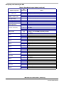
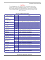
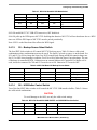
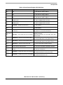
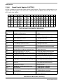
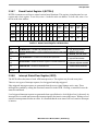
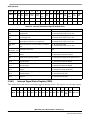
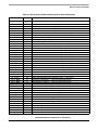
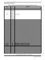
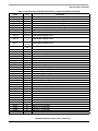
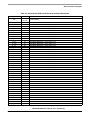
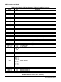
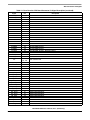
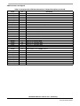
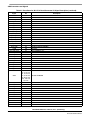
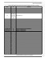
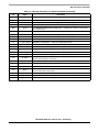
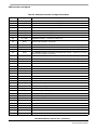
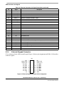
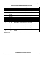
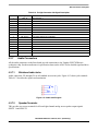
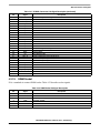
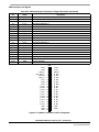
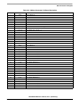
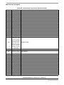
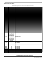
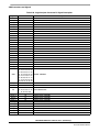
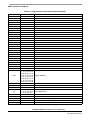
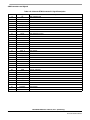
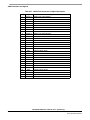
Table 3-9. Board Control Register 2 Bit Definitions
Name
Description
Settings
USELA
Bit 0
UART A SELECT — Select UART A source on the
CPU.
0 = the source is UART1 signals
1 = the source is UART5 signals
USELB
Bit 1
UART B SELECT — Select UART B source on the
CPU.
0 = the source is UART3 signals
1 = the source is UART4 signals
USELC
Bit 2
UART C SELECT — Select UART C source on the
CPU
0 = the source is UART2 signals
1 = the source is UART1 signals
UMODENA
Bit 3
UART A MODEM Enable — Enable UART A
MODEM signals.
0 = UART C MODEM signals enabled
1 = UART C MODEM signals disabled
UMODENC
Bit 4
UART C MODEM Enable — Enable UART C
MODEM signals
0 = UART C MODEM signals enabled
1 = UART C MODEM signals disabled
CSI_EN
Bit 5
CSI Enable — Enable the CSI Interface.
0 = CSI enabled
1 = CSI disabled
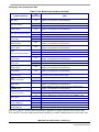
ATA_EN
Bit 6
ATA_Enable — Enable the ATA interface.
0 = ATA enabled
1 = ATA disabled
ATA_SEL
Bit 7
ATA Select — Select CPU signals connected to the
ATA interface.
0 = group A is connected to ATA interface
1 = group B is connected to ATA interface
IRDA_MOD
Bit 8
IRDA Mode — Select IRDA Transceiver bandwidth
A transition from high to low while IRDA_TXD is low –
SIR/MIR bandwidth
A transition from high to low while IRDA_TXD is high –
FIR bandwidth
LCDRST0
Bit 9
LCD 0 Reset — Reset the smart parallel LCD #1
0 = smart parallel LCD #1 reset signal negated
1 = smart parallel LCD #1 reset signal asserted
LCDRST1
Bit 10
LCD 1 Reset — Reset the smart parallel LCD #2
0 = smart parallel LCD #2 reset signal negated
1 = smart parallel LCD #2 reset signal asserted
LCDRST2
Bit 11
LCD 2 Reset — Reset the smart serial LCD
0 = smart serial LCD reset signal negated
1 = smart serial LCD reset signal asserted
LCDIO_EN
Bit 12
LCD GPIO Enable — Enable GPIO1 and GPIO2
interface with the LCD connectors
0= connection with GPIO1 and GPIO2 is enabled
1= connection with GPIO1 and GPIO2 is disabled
CT_CS
Bit 13
Code Test Chip Select — Select the Code Test
emulator
0= Code Test selected
1= Code Test not Selected
VPPEN
Bit 14
VPP Enable — Enable VPP power for the PCMCIA.
0= PCMCIA VPP power is off
1= PCMCIA VPP power is VCC power (3.3V)
VCCEN
Bit 15
VCC Enable — Enable VCC power for the PCMCIA.
0= PCMCIA VCC power is off
1= PCMCIA VCC power is 3.3V
i.MX31ADS User’s Manual, REV 1 (Preliminary)
Freescale Semiconductor
3-11