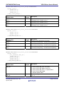
1
APPLICATION NOTE
SH7268/SH7269 Group
Video Display Controller 4 Driver User’s Manual
R01AN0778EJ0100
Rev.1.00
Apr 18, 2013
Introduction
This document explains the usage of SH7268/SH7269 Video Display Controller 4 (hereafter referred to as ‘VDC4’)
Driver.
Target Device
SH7268/SH7269
Contents
1.
Overview ........................................................................................................................................... 2
2.
API..................................................................................................................................................... 9
3.
User-defined Functions ................................................................................................................... 82
4.
Example Usage ............................................................................................................................... 87
R01AN0778EJ0100 Rev.1.00
Apr 18, 2013
Page 1 of 105
SH7268/SH7269 Group
1.
1.1
VDC4 Driver User’s Manual
Overview
Environment
This program was developed and tested in the following environments.
• CPU
⎯ SH7269
• Development Environment
⎯ HEW (SuperH RISC engine microcomputer software integrated development environment) Version 4.09.00.007
⎯ Renesas SuperH RISC engine Standard Toolchain Version 9.4.1.0
• SH C/C++ Compiler Version 9.04.01
• SH Assembler Version 7.01.02
• SH C/C++ Standard Library Generator Version 3.00.03
• Optimizing Linkage Editor Version 10.01.00
• Evaluation Board
⎯ SH7269 CPU board (Part number: R0K572690C000BR)
⎯ Optional board for graphic display (Part number: M3A-HS64G02)
⎯ SH7269 VDC4 board (Part number: R0K572690B000BR)
R01AN0778EJ0100 Rev.1.00
Apr 18, 2013
Page 2 of 105
SH7268/SH7269 Group
1.2
VDC4 Driver User’s Manual
Features
The following table lists the features supported by this driver program.
Table 1 Features of VDC4 Driver
Input Video
Picture Recording
•
•
•
•
•
•
•
•
Scaling / Rotation
•
Layer
•
•
Image Format
•
Image Synthesizer
•
Image Specification
Image Quality
Adjustment
Graphics
•
•
Panel Output
Size
•
Format
•
•
Adjustment
•
•
Notes: 1. Graphics 1 and Video are exclusive.
2.
Only for graphics 1.
R01AN0778EJ0100 Rev.1.00
Apr 18, 2013
ITU-R BT.656 standard 8bit (27MHz)
ITU-R BT.601 standard 8bit (27MHz, interlace signal)
ITU-R BT.601 standard 8bit (54MHz, progressive signal)
RGB888, RGB666 and RGB565 video image
Horizontal noise reduction
Black stretch
Sharpness / LTI
YCC422, RGB565, RGB888 format
A rate of 1/1, 1/2, 1/4 or 1/8 field
Scaling input video image to output image
Vertical / Horizontal: x1/8 to x8
0, 90, 180 or 270 degree rotation and horizontal mirroring
3 planes
Graphics 1 / Video1
Graphics 2
Graphics 3
Progressive format
RGB565, RGB888, ARGB1555, ARGB4444, ARGB8888
CLUT8, CLUT4, CLUT1, YCC4222
Alpha blending in rectangular area (fade-in and fade-out
functions)
Chroma-key
Alpha blending in one pixel units
QVGA, WQVGA, VGA, WVGA, SVGA
Progressive RGB565 / RGB666 / RGB888
Progressive RGB888 (serial output format)
Brightness / Contrast / Dither processing
RGB gamma correction
Page 3 of 105
SH7268/SH7269 Group
1.3
VDC4 Driver User’s Manual
File Configuration
The file configuration of this driver is shown below.
Table 2 File Configuration
File Name
vdc4_api.c
vdc4_api.h
vdc4_clk.c
vdc4_int.c
vdc4_local.h
vdc4_para.c
vdc4_reg.c
vdc4_user.h
Description
Source file for VDC4 driver functions.
Header file including the prototype declarations for the VDC4
driver calls and definitions of constants.
Source file for checking panel clock and software reset.
Source file interrupt handlers.
Header file including local definitions.
Source file checking arguments.
Source file controlling registers.
Header file for compilation option.
This driver requires external header files as below.
Table 3 External File Dependencies
File Name
typedefine.h
iodefine.h
1.4
Description
Header file including the typedef declarations for the basic types.
Header file including IO definitions.
Program Size and Section
Table 4 shows program size and section used by the VDC4 driver.
Table 4 Program Size and Section
"Renesas SuperH RISC engine Standard Toolchain 9.4.1.0"
"Speed & size optimization enabled"
Type
Section name
Size [byte]
Description
ROM
P_VDC4
10.3K (14.4K) Program area
C_VDC4
0.9K (1.0K) Constant area
D_VDC4
40 (40) Initialized data area
RAM
B_VDC4
204 (204) Uninitialized data area
Note: Program size does not include VRAM size and Input Video Buffer size.
Values in the parentheses are program size when parameter checking is defined.
R01AN0778EJ0100 Rev.1.00
Apr 18, 2013
Page 4 of 105
SH7268/SH7269 Group
1.5
VDC4 Driver User’s Manual
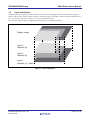
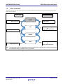
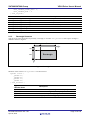
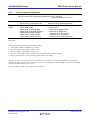
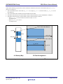
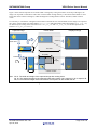
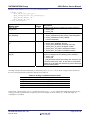
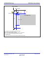
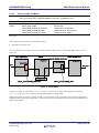
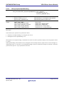
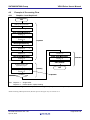
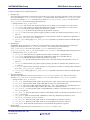
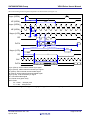
Layer and Surface
VDC4 has three layers (graphics plane). This driver uses these layers as graphics resource and creates three graphics
surfaces and one video surface. Graphics surface 1 and Video surface are mutually exclusive, because both surfaces use
layer 1 as resource. Thus, those surfaces can not be created simultaneously.
The features of VDC4 module are implemented in this driver by controlling the surfaces.
Display Image
Layer 3
Graphics (3)
Layer 2
Graphics (2)
Layer 1
Graphics (1) / Video
Figure 1 Layer and Surface
R01AN0778EJ0100 Rev.1.00
Apr 18, 2013
Page 5 of 105
SH7268/SH7269 Group
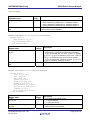
1.6
VDC4 Driver User’s Manual
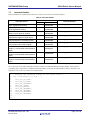
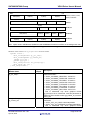
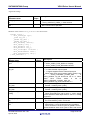
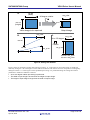
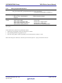
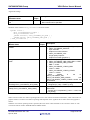
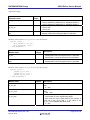
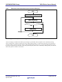
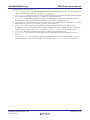
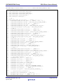
State Transitions
All surfaces have a state. The state transitions occur when a particular API function is used. The state transition of the
surface is shown below.
STATUS
API Function
Undef
VDC4_Terminate
VDC4_Initialize
Init
VDC4_DestroySurface
VDC4_GraphicsCreateSurface
&
VDC4_VideoCreateSurface
Ready
Run
VDC4_StopSurface
VDC4_GraphicsStartSurface
&
VDC4_VideoStartSurface
Note: The state of the surface is independent of each other with the exception that the states of all surfaces
are changed by VDC4_Initialize or VDC4_Terminate.
Figure 2 VDC4 Driver State Transitions
R01AN0778EJ0100 Rev.1.00
Apr 18, 2013
Page 6 of 105
SH7268/SH7269 Group
1.7
VDC4 Driver User’s Manual
Interrupt Handler
Interrupt handlers are implemented in this driver. Table 5 shows the list of interrupt handlers.
Table 5 Interrupt Handler
Interrupt Source
VI_VSYNC
Vsync signal before scaling
LO_VSYNC
Vsync signal after scaling
VSYNCERR
Missing Vsync signal for scaling
VLINE
Specified line signal for panel output
VFIELD
Field end signal for recording function
VBUFERR1
Frame buffer write overflow signal
VBUFERR2
Graphics 1 frame buffer read underflow
signal
VBUFERR3
Graphics 2 frame buffer read underflow
signal
VBUFERR4
Graphics 3 frame buffer read underflow
signal
Interrupt Vector
Number
Address
171
0x000002AC ~
0x000002AF
172
0x000002B0 ~
0x000002B3
173
0x000002B4 ~
0x000002B7
174
0x000002B8 ~
0x000002BB
175
0x000002BC ~
0x000002BF
176
0x000002C0 ~
0x000002C3
177
0x000002C4 ~
0x000002C7
Interrupt Handler
void vdc4_Int_VI_VSYNC( void ) ;
void vdc4_Int_LO_VSYNC( void ) ;
void vdc4_Int_VSYNCERR( void ) ;
void vdc4_Int_VLINE( void ) ;
void vdc4_Int_VFIELD( void ) ;
void vdc4_Int_VBUFERR1( void ) ;
void vdc4_Int_VBUFERR2( void ) ;
178
0x000002C8 ~
0x000002CB
void vdc4_Int_VBUFERR3( void ) ;
179
0x000002CC ~
0x000002CF
void vdc4_Int_VBUFERR4( void ) ;
If it is necessary to use VDC4 interrupts, functions in Table 5 should be defined as interrupt handler. If API function
provided by OS or equal with it to define the interrupt handler is not used, interrupt handler in Table 5 should be set to
appropriate entry in the vector table (see example below).
1
2
3
4
5
6
7
8
9
10
11
12
13
14
15
/* Vector table example */
/* Register the interrupt handler in the vector table */
void (*VectorTable[])( void ) = {
…
vdc4_Int_VI_VSYNC,
vdc4_Int_LO_VSYNC,
vdc4_Int_VSYNCERR,
vdc4_Int_VLINE,
vdc4_Int_VFIELD,
vdc4_Int_VBUFERR1,
vdc4_Int_VBUFERR2,
vdc4_Int_VBUFERR3,
vdc4_Int_VBUFERR4,
…
} ;
R01AN0778EJ0100 Rev.1.00
Apr 18, 2013
Page 7 of 105
SH7268/SH7269 Group
1.8
VDC4 Driver User’s Manual
Compilation Switches
This driver has compilation switches in vdc4_user.h.
1.8.1
Parameter Checking
When _VDC4_PARAMETER_CHECK is defined, the driver checks the arguments of driver functions. Arguments are
checked and error codes returned if there are errors. For error codes, see 2.2 Error and 2.3 API Function.
1.8.2
Interrupt Handler Definition
In this driver, some functions for interrupt handlers are implemented (see 1.7 Interrupt Handler and Table 5). To use
these functions for interrupt function that will guarantee register values before and after processing,
_VDC4_DEFINE_INTHDL should be defined. When _VDC4_DEFINE_INTHDL is defined, the declaration "#pragma
interrupt" is enabled and the compiler assumes that the functions in Table 5 are interrupt functions.
If some function that support interrupt function (e.g. the API function provided by OS to register the interrupt handler)
is used for the registration of the interrupt handler, _VDC4_DEFINE_INTHDL should be undefined.
1.9
1.9.1
Restriction
Reserved Word
To separate from the other program, the prefix ‘VDC4’ is appended to the API names, variable names and other
symbols in this driver. Therefore, the names started with ‘VDC4’ (in both uppercase and lowercase letters) should not
be used in the other program.
1.9.2
Register Update
A lot of VDC4 registers are updated at the rising edge of the Vsync signal. Therefore, it will take a period of time equal
to 1 Vsync period time at the most to reflect the set values.
1.9.3
Reentrancy
API functions in this driver are not reentrant. If API functions are called asynchronously from multiple tasks or interrupt
service routines, it can cause unexpected behavior. Pay attention to where and when API functions are called.
R01AN0778EJ0100 Rev.1.00
Apr 18, 2013
Page 8 of 105
SH7268/SH7269 Group
2.
VDC4 Driver User’s Manual
API
2.1
2.1.1
Common Definition
Typedef
In this driver, data types in Table 6 are used. These declarations are defined in typedefine.h (see 1.3File Configuration).
Table 6 Typedef Declarations
Typedef
_SBYTE
_UBYTE
_SWORD
_UWORD
_SINT
_UINT
_SDWORD
_UDWORD
_SQWORD
_UQWORD
2.1.2
Type
signed char
unsigned char
signed short
unsigned short
signed int
unsigned int
signed long
unsigned long
signed long long
unsigned long long
Definition of Enumeration Constants
The vdc4_OnOff enumeration defines ON and OFF.
typedef enum {
VDC4_OFF = 0,
VDC4_ON = 1
} vdc4_OnOff ;
Enum
VDC4_OFF
VDC4_ON
Value
0
1
Description
OFF
ON
The vdc4_Edge enumeration defines the edge of the signal.
typedef enum {
VDC4_EDGE_RISING = 0,
VDC4_EDGE_FALLING = 1
} vdc4_Edge ;
Enum
VDC4_EDGE_RISING
VDC4_EDGE_FALLING
Value
0
1
Description
rising edge of the signal
falling edge of the signal
The vdc4_LayerID enumeration defines the surface ID.
typedef enum {
VDC4_SURFACE_GRAPHICS_1 =
VDC4_SURFACE_GRAPHICS_2 =
VDC4_SURFACE_GRAPHICS_3 =
VDC4_SURFACE_GRAPHICS_NUM
VDC4_SURFACE_VIDEO_1 = 3,
R01AN0778EJ0100 Rev.1.00
Apr 18, 2013
0,
1,
2,
= 3,
Page 9 of 105
SH7268/SH7269 Group
VDC4 Driver User’s Manual
VDC4_SURFACE_VIDEO_NUM = 1,
VDC4_SURFACE_NUM = 4
} vdc4_LayerID ;
Enum
VDC4_SURFACE_GRAPHICS_1
VDC4_SURFACE_GRAPHICS_2
VDC4_SURFACE_GRAPHICS_3
VDC4_SURFACE_GRAPHICS_NUM
VDC4_SURFACE_VIDEO_1
VDC4_SURFACE_VIDEO_NUM
VDC4_SURFACE_NUM
2.1.3
Value
0
1
2
3
3
1
4
Description
Graphics 1 surface ID
Graphics 2 surface ID
Graphics 3 surface ID
Number of Graphics surfaces
Video surface ID
Number of Video surfaces
Number of surfaces
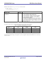
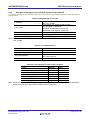
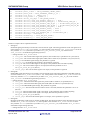
Rectangle Structure
This driver has some timing data expressed by a rectangle, so structure vdc4_AreaRect that express rectangle is
defined as shown in Figure 3.
hs
hw
vs
vw
Rectangle
Figure 3 Rectangle Data
Members of the structure vdc4_AreaRect are shown below.
typedef struct {
_UWORD hs ;
_UWORD hw ;
_UWORD vs ;
_UWORD vw ;
} vdc4_AreaRect ;
Type
Member Name
_UWORD hs
_UWORD hw
_UWORD vs
_UWORD vw
R01AN0778EJ0100 Rev.1.00
Apr 18, 2013
Description
Horizontal start position [pixel clock cycles]
Horizontal width [pixel clock cycles]
Vertical start position [lines]
Height ( vertical width ) [lines]
Page 10 of 105
SH7268/SH7269 Group
2.2
VDC4 Driver User’s Manual
Error
API function calls returns an error code. The error codes are shown in Table 7.
Table 7 Error Code List
Error
VDC4_ERR_NONE
Value
0
VDC4_ERR_SURFACE_BAD
0x2000
VDC4_ERR_SURFACE_STATUS
0x2001
VDC4_ERR_PARAM_RANGE
0x4001
VDC4_ERR_PARAM_UNDEF
0x4002
VDC4_ERR_PARAM_INVALID
0x4003
VDC4_ERR_PARAM_OTHERS
0x4000
VDC4_ERR_SYSTEM_PNLCLK
0x8000
Description
Normal end.
Surface error. The function cannot be called
with the surface.
Surface error. The function cannot be called
in a current state.
Parameter error. The specified value is out
of range.
Parameter error. Null should not be
specified.
Parameter error. The specified parameter is
invalid.
Parameter error. Others.
System error. The abnormality of the panel
clock is detected.
Parameter errors are returned from API function call only when the compilation switch of parameter checking is defined.
R01AN0778EJ0100 Rev.1.00
Apr 18, 2013
Page 11 of 105
SH7268/SH7269 Group
2.3
VDC4 Driver User’s Manual
API Function
Table 8 shows the states in which each driver call can be made.
Table 8 State Matrix
Driver Call Name
VDC4_Initialize
VDC4_Terminate
VDC4_GraphicsCreateSurface
VDC4_VideoCreateSurface
VDC4_DestroySurface
VDC4_RegistCallbackFunc
VDC4_GraphicsStartSurface
VDC4_VideoStartSurface
VDC4_GraphicsChangeParam
VDC4_VideoChangeParam
VDC4_StopSurface
VDC4_ImageColorMatrix
VDC4_VideoNoiseReduction
VDC4_ImageEnhancement
VDC4_GraphicsAlphaBlending
VDC4_GraphicsChromakey
VDC4_GraphicsSetCLUT
VDC4_DisplayCalibration
VDC4_DisplaySetGammaCorrectionTable
VDC4_SwitchVsync
VDC4_CheckClock
VDC4_Reset
R01AN0778EJ0100 Rev.1.00
Apr 18, 2013
Surface
All surface
All surface
Video
Graphics1/2/3
Video
Graphics 1/2/3
All surface
All surface
Video
Graphics 1/2/3
Video
Graphics 1/2/3
Video
Graphics 1/2/3
Video
Graphics 1/2/3
All surface
Video
Graphics 1
Graphics 2/3
Video
Graphics 1/2/3
Video
Graphics 1
Graphics 2/3
Video
Graphics 1
Graphics 2/3
Video
Graphics 1
Graphics 2/3
Video
Graphics 1/2/3
All surface
All surface
All surface
All surface
All surface
Undef
OK
NG
NG
NG
NG
NG
States
Init
Ready
NG
OK
NG
OK
OK
NG
NG
NG
NG
NG
NG
NG
NG
OK
OK
NG
OK
OK
NG
OK
NG
NG
NG
NG
NG
NG
NG
NG
NG
NG
NG
NG
NG
NG
NG
NG
NG
OK
OK
NG
OK
NG
OK
OK
NG
NG
NG
OK
NG
NG
OK
NG
OK
OK
OK
OK
NG
NG
NG
NG
NG
NG
NG
NG
NG
NG
NG
NG
NG
OK
OK
Run
NG
NG
NG
NG
NG
OK
OK
NG
OK
NG
NG
OK
OK
NG
NG
NG
OK
NG
NG
OK
NG
OK
Page 12 of 105
SH7268/SH7269 Group
2.3.1
Syntax
VDC4 Driver User’s Manual
VDC4_Initialize
#include
"vdc4_api.h"
vdc4_ErrorCode VDC4_Initialize( const vdc4_InitAttr *attr,
void (*init_func)( _UDWORD ),
_UDWORD user_num ) ;
Parameters •
•
•
Return
•
Values
[in]const vdc4_InitAttr *attr
[in]void (*init_func)( _UDWORD )
[in]_UDWORD user_num
vdc4_ErrorCode
VDC4_ERR_NONE
VDC4_ERR_PARAM_RANGE
VDC4_ERR_PARAM_UNDEF
VDC4_ERR_PARAM_INVALID
VDC4_ERR_PARAM_OTHERS
Initialization attribute parameter
Pointer to the user-defined function
User-defined number
Error code
Normal end.
Parameter error. Out of range.
Parameter error. Undefined.
Parameter error. Invalid parameter.
Parameter error. Others.
Description
In this function, the operations are performed as below.
•
•
•
•
•
•
•
The specified user-defined function is executed.
The VDC4 driver internal variables are initialized.
The VDC4 registers are initialized.
The initialization for LCD panel drive is performed.
The operation of the panel clock is enabled.
The VDC4 interrupts are enabled.
All states of surfaces are transitioned to ‘Init’.
Before VDC4 driver initialization, user-defined function specified by init_func is called. For information about the
process of user-defined function, see 3.1.
It is not always necessary to specify the user-defined function pointer. If user-defined function is not specified, the
operation stated below should be performed before this VDC4 driver initialization.
•
•
•
•
Supply the clock to the VDC4.
Set the VDC4 interrupt levels.
Set I/O port for the VDC4.
Set the environment specific parameters (e.g. related to input video image or LCD panel).
R01AN0778EJ0100 Rev.1.00
Apr 18, 2013
Page 13 of 105
SH7268/SH7269 Group
VDC4 Driver User’s Manual
Arguments Settings
Type
Parameter Name
vdc4_InitAttr *
attr
void
(*init_func)( _UDWORD )
Description
Input /
Output
in
Initialization attribute parameter
NULL should not be specified.
Pointer to the user-defined function
If ‘0’ is not specified, user-defined function will be called
with an argument specified by user-defined number
(user_num). If necessary, user-defined function must be
implemented by the user.
in
Syntax
void Init_Func( _UDWORD User_Num ) ;
Parameters
_UDWORD
user_num
• [in]_UDWORD
User_Num
• void
User-defined
number
Return
Values
Description
Processing implemented by the user is performed.
User-defined number
This parameter is used as an argument to the userdefined function. This parameter is ignored, when pointer to
the user-defined function (init_func) is set to ‘0’.
in
Members of the structure vdc4_InitAttr are shown below.
typedef struct {
vdc4_VsyncSigSel Vsel ;
vdc4_SyncCtrl *sync ;
vdc4_PanelClockSel panel_icksel ;
vdc4_PanelClkDCDR panel_dcdr ;
_UWORD tcon_half ;
_UWORD tcon_offset ;
vdc4_Edge outcnt_lcd_edge ;
vdc4_LcdTconTim *outctrl[ VDC4_LCD_TCONSIG_NUM ] ;
vdc4_LcdOutput *settings ;
_UDWORD IntEnable_1 ;
_UDWORD IntEnable_2 ;
} vdc4_InitAttr ;
Type
Member Name
vdc4_VsyncSigSel
Vsel
vdc4_SyncCtrl *
sync
vdc4_PanelClockSel
panel_icksel
R01AN0778EJ0100 Rev.1.00
Apr 18, 2013
Input /
Output
in
in
in
Description
Vsync Signal Output Select
Synchronization Control
If NULL is specified, the frequent Vsync signal
masking and the missing Vsync signal compensation
will be set to turn off.
Panel clock source select
• VDC4_LCDPANEL_CLKSEL_IMG:
Page 14 of 105
SH7268/SH7269 Group
VDC4 Driver User’s Manual
vdc4_PanelClkDCDR
panel_dcdr
in
_UWORD
tcon_half
in
_UWORD
tcon_offset
in
vdc4_Edge
outcnt_lcd_edge
in
vdc4_LcdTconTim *
outctrl[ VDC4_LCD_TCONSIG_NUM ]
in
vdc4_LcdOutput *
settings
_UDWORD
IntEnable_1
in
R01AN0778EJ0100 Rev.1.00
Apr 18, 2013
in
Video image clock (VIDEO_X1)
• VDC4_LCDPANEL_CLKSEL_EXT:
External clock (LCDEXT_CLK)
• VDC4_LCDPANEL_CLKSEL_PERI:
Peripheral clock 1
• VDC4_LCDPANEL_CLKSEL_IMG_DV:
Video image clock (DV_CLK)
Panel clock frequency division ratio
• VDC4_LCDPANEL_CLKDIV_1_1: 1/1
• VDC4_LCDPANEL_CLKDIV_1_2: 1/2
• VDC4_LCDPANEL_CLKDIV_1_3: 1/3
• VDC4_LCDPANEL_CLKDIV_1_4: 1/4
• VDC4_LCDPANEL_CLKDIV_1_5: 1/5
• VDC4_LCDPANEL_CLKDIV_1_6: 1/6
• VDC4_LCDPANEL_CLKDIV_1_7: 1/7
• VDC4_LCDPANEL_CLKDIV_1_8: 1/8
• VDC4_LCDPANEL_CLKDIV_1_9: 1/9
• VDC4_LCDPANEL_CLKDIV_1_12: 1/12
• VDC4_LCDPANEL_CLKDIV_1_16: 1/16
• VDC4_LCDPANEL_CLKDIV_1_24: 1/24
• VDC4_LCDPANEL_CLKDIV_1_32: 1/32
TCON reference timing, 1/2fH timing
The clock cycle count from the Hsync rising edge.
0x0000 ~ 0x07FF
TCON reference timing, offset Hsync signal timing
The clock cycle count from the Hsync rising edge.
0x0000 ~ 0x07FF
Output phase control of LCD_DATA23 to LCD_DATA0
pin
• VDC4_EDGE_RISING: Rising edge
• VDC4_EDGE_FALLING: Falling edge
LCD TCON timing setting
• outctrl[VDC4_LCD_TCONSIG_STVA_VS]:
STVA / VS
• outctrl[VDC4_LCD_TCONSIG_STVB_VE]:
STVB / VE
• outctrl[VDC4_LCD_TCONSIG_STH_SP_HS]:
STH / SP / HP
• outctrl[VDC4_LCD_TCONSIG_STB_LP_HE]:
STB / LP / HE
• outctrl[VDC4_LCD_TCONSIG_CPV_GCK]:
CPV / GCK
• outctrl[VDC4_LCD_TCONSIG_POLA]: POLA
• outctrl[VDC4_LCD_TCONSIG_POLB]: POLB
• outctrl[VDC4_LCD_TCONSIG_DE]: DE
The settings of unnecessary signal should be set to
NULL.
LCD Output Control
NULL should not be specified.
Interrupt enable bits 1, INT 0 - INT 7
Specify the interrupt to be used. To use more than
one type of interrupt, the OR should be taken to specify
the value.
Page 15 of 105
SH7268/SH7269 Group
_UDWORD
IntEnable_2
VDC4 Driver User’s Manual
in
• VDC4_INT_BIT_NONE: None
• VDC4_INT_BIT_VI_VSYNC: VI_VSYNC
• VDC4_INT_BIT_LO_VSYNC: LO_VSYNC
• VDC4_INT_BIT_VSYNCERR: VSYNCERR
• VDC4_INT_BIT_VLINE: VLINE
• VDC4_INT_BIT_VFIELD: VFIELD
• VDC4_INT_BIT_VBUFERR1: VBUFFER1
• VDC4_INT_BIT_VBUFERR2: VBUFFER2
• VDC4_INT_BIT_VBUFERR3: VBUFFER3
Interrupt enable bits 2, INT 8
If necessary, specify VBUFFER4 interrupt.
• VDC4_INT_BIT_NONE: None
• VDC4_INT_BIT_VBUFERR4: VBUFFER4
Members of the structure vdc4_VsyncSigSel are shown below.
typedef struct {
vdc4_OnOff FreeRunVsync ;
_UWORD res_fv ;
_UWORD res_fh ;
} vdc4_VsyncSigSel ;
Type
Member Name
vdc4_OnOff
FreeRunVsync
Input/
Output
in
_UWORD
res_fv
in
_UWORD
res_fh
in
Description
Free-running Vsync ON/OFF
• VDC4_OFF
• VDC4_ON
Free-running Vsync period setting
Vsync period = (res_fv + 1) x Hsync period
0x0000 ~ 0x07FF [lines]
This parameter is ignored, when Free-running Vsync
(FreeRunVsync) is set to VDC4_OFF.
Hsync period setting
Hsync period = (res_fh + 1) / pixel clock frequency
0x0000 ~ 0x07FF [pixel clock cycles]
Members of the structure vdc4_SyncCtrl are shown below.
typedef struct {
vdc4_OnOff res_vmask_on ;
_UWORD res_vmask ;
vdc4_OnOff res_vlack_on ;
_UWORD res_vlack ;
} vdc4_SyncCtrl ;
Type
Member Name
vdc4_OnOff
res_vmask_on
_UWORD
res_vmask
R01AN0778EJ0100 Rev.1.00
Apr 18, 2013
Input/
Output
in
in
Description
Repeated Vsync signal masking control
• VDC4_OFF
• VDC4_ON
Repeated Vsync signal masking period
res_vmask should be specified in terms of 128 pixel
clock cycles.
Page 16 of 105
SH7268/SH7269 Group
VDC4 Driver User’s Manual
vdc4_OnOff
res_vlack_on
in
_UWORD
res_vlack
in
Missing Vsync signal compensation
• VDC4_OFF
• VDC4_ON
Missing-Sync Compensating pulse output wait time
res_vlack should be specified in terms of 128 pixel
clock cycles.
Members of the structure vdc4_LcdTconTim are shown below.
typedef struct {
_UWORD tcon_hsvs ;
_UWORD tcon_hwvw ;
vdc4_LcdTconPolMode tcon_md ;
_UWORD tcon_hs_sel ;
_UWORD tcon_inv ;
vdc4_LcdTconPin tcon_pin ;
vdc4_Edge outcnt_edge ;
} vdc4_LcdTconTim ;
Type
Member Name
_UWORD
tcon_hsvs
Input/
Output
in
_UWORD
tcon_hwvw
in
vdc4_LcdTconPolMode
tcon_md
in
_UWORD
tcon_hs_sel
in
_UWORD
tcon_inv
in
vdc4_LcdTconPin
tcon_pin
in
R01AN0778EJ0100 Rev.1.00
Apr 18, 2013
Description
Signal pulse start position
First changing timing. Starts pulse output after the
time specified by the value of tcon_hsvs.
0x0000 ~ 0x07FF [pixel clock cycles or 1/2fH cycles]
This parameter should be greater than or equal to 1
when tcon_md of POLA/POLB signal is not set to
normal mode.
Pulse width
Second changing timing. Outputs a pulse of the
duration of the value of tcon_hwvw.
0x0000 ~ 0x07FF [pixel clock cycles or 1/2fH cycles]
POLA/POLB signal generation mode select
• VDC4_LCD_TCON_POLMD_NORMAL:
Normal mode
• VDC4_LCD_TCON_POLMD_1X1REV:
1x1 reverse mode
• VDC4_LCD_TCON_POLMD_1X2REV:
1x2 reverse mode
• VDC4_LCD_TCON_POLMD_2X2REV:
2x2 reverse mode
Horizontal signal operating reference select
• 0: Hsync signal reference
• 1: Offset Hsync signal reference
Offset value is specified by the tcon_offset member
of the vdc4_InitAttr structure.
Polarity inversion control of signal
• 0: Not inverted
• 1: Inverted
Output pin for LCD driving signal
• VDC4_LCD_TCON_PIN_NON: None
• VDC4_LCD_TCON_PIN_0: LCD_TCON0
• VDC4_LCD_TCON_PIN_1: LCD_TCON1
• VDC4_LCD_TCON_PIN_2: LCD_TCON2
Page 17 of 105
SH7268/SH7269 Group
VDC4 Driver User’s Manual
• VDC4_LCD_TCON_PIN_3: LCD_TCON3
• VDC4_LCD_TCON_PIN_4: LCD_TCON4
• VDC4_LCD_TCON_PIN_5: LCD_TCON5
• VDC4_LCD_TCON_PIN_6: LCD_TCON6
vdc4_Edge
in
Output phase control of signal
outcnt_edge
• VDC4_EDGE_RISING: Rising edge
• VDC4_EDGE_FALLING: Falling edge
This parameter is not referenced when the output pin
(tcon_pin) is set to VDC4_LCD_TCON_PIN_NON.
Note: Specify tcon_hsvs and tcon_hwvw in pixel clock cycles when the signal is used as horizontal signal.
Specify tcon_hsvs and tcon_hwvw in 1/2fH cycles when the signal is used as vertical signal.
It is not necessary to set all member of the structure vdc4_LcdTconTim. Members that must be set are different
depending on the each signal.
Table 9 Structure vdc4_LcdTconTim and Timing Signal
Signal
STVA
STVB
STH
STB
Member
tcon_hsvs
R
R
R
R
tcon_hwvw
R
R
R
R
tcon_md
I
I
I
I
tcon_hs_sel
I
I
R
R
tcon_inv
R
R
R
R
tcon_pin
R
R
R
R
outcnt_edge
R
R
R
R
Note: ‘R’ in the table means that the member is referred.
‘I’ in the table means that the member is ignored.
CPV
POLA
POLB
DE
R
R
I
R
R
R
R
R
R
R
R
R
R
R
R
R
R
R
R
R
R
I
I
I
I
R
R
R
Members of the structure vdc4_LcdOutput are shown below.
typedef struct {
vdc4_AreaRect res_f ;
vdc4_OnOff out_endian_on ;
vdc4_OnOff out_swap_on ;
vdc4_LcdOutFormat out_format ;
vdc4_LcdClkFrqSel out_frq_sel ;
_UWORD out_dir_sel ;
vdc4_LcdClkPhase out_phase ;
} vdc4_LcdOutput ;
Type
Member Name
vdc4_AreaRect
res_f
Input/
Output
in
vdc4_OnOff
out_endian_on
in
vdc4_OnOff
in
R01AN0778EJ0100 Rev.1.00
Apr 18, 2013
Description
Full-screen enable control
See section 2.1.3 for the structure vdc4_AreaRect.
res_f.hs should be 16 clock cycles or greater.
res_f.hs + res_f.hw should be 2015 clock cycles or less.
res_f.vs should be 4 lines or greater. res_f.vs +
res_f.vw should be 2039 lines or less.
Bit endian change ON/OFF control
• VDC4_OFF
• VDC4_ON
B/R signal swap ON/OFF control
Page 18 of 105
SH7268/SH7269 Group
VDC4 Driver User’s Manual
out_swap_on
vdc4_LcdOutFormat
out_format
in
vdc4_LcdClkFrqSel
out_frq_sel
in
_UWORD
out_dir_sel
in
vdc4_LcdClkPhase
out_phase
in
R01AN0778EJ0100 Rev.1.00
Apr 18, 2013
• VDC4_OFF
• VDC4_ON
LCD output format select
• VDC4_LCD_OUTFORMAT_RGB888: RGB888
• VDC4_LCD_OUTFORMAT_RGB666: RGB666
• VDC4_LCD_OUTFORMAT_RGB565: RGB565
• VDC4_LCD_OUTFORMAT_SERIAL_RGB:
Serial RGB
Clock frequency control
• VDC4_LCD_SERIAL_CLKFRQ_3: x 3, serial RGB
• VDC4_LCD_SERIAL_CLKFRQ_4: x 4, serial RGB
This parameter is referenced only when LCD output
format select (out_format) is set to serial RGB.
Scan direction select
• 0: Forward scan
• 1: Reverse scan
This parameter is referenced only when LCD output
format select (out_format) is set to serial RGB.
Clock Phase Adjustment for Serial RGB Output
Triple speed mode (x3)
• VDC4_LCD_SERIAL_CLKPHASE_0: 0[clk]
• VDC4_LCD_SERIAL_CLKPHASE_1: 1[clk]
• VDC4_LCD_SERIAL_CLKPHASE_2: 2[clk]
Quadruple speed mode (x4)
• VDC4_LCD_SERIAL_CLKPHASE_0: 0[clk]
• VDC4_LCD_SERIAL_CLKPHASE_1: 1[clk]
• VDC4_LCD_SERIAL_CLKPHASE_2: 2[clk]
• VDC4_LCD_SERIAL_CLKPHASE_3: 3[clk]
This parameter is referenced only when LCD output
format select (out_format) is set to serial RGB.
Page 19 of 105
SH7268/SH7269 Group
2.3.2
Syntax
VDC4 Driver User’s Manual
VDC4_Terminate
#include
"vdc4_api.h"
vdc4_ErrorCode VDC4_Terminate( void (*quit_func)( _UDWORD ),
_UDWORD user_num ) ;
Parameters •
•
Return
•
Values
[in]void (*quit_func)( _UDWORD )
[in]_UDWORD user_num
vdc4_ErrorCode
VDC4_ERR_NONE
VDC4_ERR_SURFACE_STATUS
Pointer to the user-defined function
User-defined number
Error code
Normal end.
Surface error. Illegal state.
Description
In this function, the operations are performed as below.
•
•
•
•
The specified user-defined function is executed.
The operation of the panel clock is disabled.
The VDC4 interrupts are disabled.
All states of surfaces are transitioned to ‘Undef’.
After VDC4 driver termination, user-defined function specified by quit_func is called. For information about the
process of user-defined function, see 3.2.
It is not always necessary to specify the user-defined function pointer. If user-defined function is not specified, the
operation stated below should be performed after this VDC4 driver termination.
• Halt the clock supply to the VDC4.
• Clear the VDC4 interrupt levels.
• Set the environment specific parameters (e.g. related to input video image or LCD panel).
R01AN0778EJ0100 Rev.1.00
Apr 18, 2013
Page 20 of 105
SH7268/SH7269 Group
VDC4 Driver User’s Manual
Arguments Settings
Type
Parameter Name
void
(*quit_func)( _UDWORD )
Input /
Output
in
Description
Pointer to the user-defined function
If ‘0’ is not specified, user-defined function will be called
with an argument specified by user-defined number
(user_num). If necessary, user-defined function must be
implemented by the user.
Syntax
void Quit_Func( _UDWORD User_Num ) ;
Parameters
_UDWORD
user_num
R01AN0778EJ0100 Rev.1.00
Apr 18, 2013
in
• [in]_UDWORD
User_Num
• void
User-defined
number
Return
Values
Description
Processing implemented by the user is performed.
User-defined number
This parameter is used as an argument to the userdefined function. This parameter is ignored, when pointer to
the user-defined function (quit_func) is set to ‘0’.
Page 21 of 105
SH7268/SH7269 Group
2.3.3
Syntax
VDC4 Driver User’s Manual
VDC4_GraphicsCreateSurface
#include
"vdc4_api.h"
vdc4_ErrorCode VDC4_GraphicsCreateSruface( vdc4_LayerID id,
const vdc4_GraphicsAttr *attr ) ;
Parameters •
•
Return
•
Values
[in]vdc4_LyerID id
[in]const vdc4_GraphicsAttr *attr
vdc4_ErrorCode
VDC4_ERR_NONE
VDC4_ERR_SURFACE_BAD
VDC4_ERR_SURFACE_STATUS
VDC4_ERR_PARAM_RANGE
VDC4_ERR_PARAM_UNDEF
VDC4_ERR_PARAM_INVALID
Layer ID
Graphics surface attribute parameter
Error code
Normal end.
Surface error. Illegal surface.
Surface error. Illegal state.
Parameter error. Out of range.
Parameter error. Undefined.
Parameter error. Invalid parameter.
Description
In this function, the operations are performed as below.
•
•
•
•
•
The graphics surface specified by id is created.
The color format of the graphics surface is set.
The frame buffer of the graphics surface is set.
The state of the graphics surface specified by id is transitioned from ‘Init’ to ‘Ready’.
Scaling up parameters are set only when graphics surface 1 is created.
If CLUT1, CLUT4 or CLUT8 color format is specified, it is necessary to set CLUT. If ARGB1555 color format is
specified, the alpha value should be specified. To set CLUT and the alpha value for ARGB1555 format are performed
by VDC4_GraphicsSetCLUT (see 2.3.17).
Note that graphics surface 1 and video surface are exclusive.
R01AN0778EJ0100 Rev.1.00
Apr 18, 2013
Page 22 of 105
SH7268/SH7269 Group
VDC4 Driver User’s Manual
Arguments Settings
Type
Parameter Name
vdc4_LayerID
id
Description
Input /
Output
in
vdc4_GraphicsAttr *
attr
Layer ID
• VDC4_SURFACE_GRAPHICS_1: Graphics surface 1
• VDC4_SURFACE_GRAPHICS_2: Graphics surface 2
• VDC4_SURFACE_GRAPHICS_3: Graphics surface 3
Graphics surface attribute parameter
NULL should not be specified.
in
Members of the structure vdc4_GraphicsAttr are shown below.
typedef struct {
vdc4_AreaRect gr_grc ;
vdc4_FrameBuff buff ;
} vdc4_GraphicsAttr ;
Type
Member Name
vdc4_AreaRect
gr_grc
Input/
Output
in
vdc4_FrameBuff
buff
in
Description
Display area
See section 2.1.3 for the structure vdc4_AreaRect.
gr_grc.hs should be 16 clock cycles or greater.
gr_grc.hs + gr_grc.hw should be 2015 clock cycles or
less. gr_grc.hw should be 3 clock cycles or greater.
gr_grc.vs should be 4 lines or greater. gr_grc.vs +
gr_grc.vw should be 2039 lines or less.
Graphics frame buffer parameter
Members of the structure vdc4_FrameBuff are shown below.
typedef struct {
_SINT gr_bst_md ;
void *gr_base ;
void *buff_2nd ;
_UWORD gr_ln_off ;
_SINT gr_ln_off_dir ;
_UWORD gr_flm_loop ;
vdc4_GrFormat gr_format ;
vdc4_OnOff gr_endian_on ;
_UDWORD bg_color ;
vdc4_GraphicsExt *GraEx ;
} vdc4_FrameBuff ;
Type
Member Name
_SINT
gr_bst_md
void *
gr_base
R01AN0778EJ0100 Rev.1.00
Apr 18, 2013
Input/
Output
in
in
Description
Frame buffer burst transfer mode
• 0: 32-byte transfer
• 1: 128-byte transfer
Frame buffer base address
NULL must not be specified.
Page 23 of 105
SH7268/SH7269 Group
VDC4 Driver User’s Manual
void *
buff_2nd
in
_UWORD
gr_ln_off
in
_SINT
gr_ln_off_dir
in
_UWORD
gr_flm_loop
in
vdc4_GrFormat
gr_format
in
vdc4_OnOff
gr_endian_on
in
_UDWORD
bg_color
in
vdc4_GraphicsExt *
GraEx
in
R01AN0778EJ0100 Rev.1.00
Apr 18, 2013
2nd frame buffer base address (only double buffering
mode)
When single buffer mode, NULL must be specified.
For more information about memory allocation for the
second buffer, see Figure 4.
Frame buffer line offset address [bytes]
When gr_bst_md is set to 0:
A multiple of 32
When gr_bst_md is set to 1:
A multiple of 128
Line offset address direction of the frame buffer
• 0: Increments the address by the line offset address.
• 1: Decrements the address by the line offset
address.
If gr_ln_off_dir is set to ‘1’, the displayed image will
be flipped vertically.
Number of lines when reading the addresses
repeatedly
The number of lines is gr_flm_loop + 1.
0x0000 (0) ~ 0x03FF (1023)
If this feature is not necessary, it’s recommended that
gr_flm_loop is set to a large value enough (e.g. 1023).
Graphics format of the frame buffer read signal
• VDC4_FORMAT_RGB565: RGB565
• VDC4_FORMAT_RGB888: RGB888
• VDC4_FORMAT_ARGB1555: ARGB1555
• VDC4_FORMAT_ARGB4444: ARGB4444
• VDC4_FORMAT_ARGB8888: ARGB8888
• VDC4_FORMAT_CLUT8: CLUT8
• VDC4_FORMAT_CLUT4: CLUT4
• VDC4_FORMAT_CLUT1: CLUT1
• VDC4_FORMAT_YCC422:
YCbCr422, only for graphics 1
Endian control of data read from buffer (ON/OFF)
• VDC4_OFF
• VDC4_ON
Background color
When gr_format is set to CLUT1, CLUT4, CLUT8 or
YCbCr422, specify value in RGB888 format.
Except as noted above, specify value in the same
color format specified by gr_format.
LSB-justified format.
See Figure 5 for the background color format.
Graphics Extension parameter
This is valid only when Graphics 1 is specified.
If it is unnecessary, GraEx can be NULL.
Page 24 of 105
SH7268/SH7269 Group
VDC4 Driver User’s Manual
When double buffering is performed, note the limitations stated below about the second frame buffer (buff_2nd)
memory (see Figure 4).
• The second buffer has the same width (gr_arc.hw), height (gr_arc.vw) and line offset (gr_ln_off) as the
first buffer has.
• The second frame buffer should be allocated behind the first buffer.
• The address offset between two frame buffer (Frame offset) should be less than ‘0x00800000’ (8.0Mbyte).
• The address offset between two frame buffer (Frame offset) should be as follows:
⎯ When gr_bst_md (frame buffer burst transfer mode) is set to 0:
A multiple of 32
⎯ When gr_bst_md is set to 1:
A multiple of 128
Frame buffer start address
gr_base
Frame offset
gr_ln_off
buff_2nd
2nd. frame buffer start address
gr_arc.hw
gr_arc.vw
A. Memory Map
B. Data Arrangement
Figure 4 Memory Allocation and Data Arrangement for the 2nd Buffer
R01AN0778EJ0100 Rev.1.00
Apr 18, 2013
Page 25 of 105
SH7268/SH7269 Group
VDC4 Driver User’s Manual
Background Color
MSB
0x00 (8bits)
R (8bits)
0x00 (16bits)
LSB
G (8bits)
R (5bits)
B (8bits)
G (6bits)
RGB888, CLUT8, CLUT4,
CLUT1, YCbCr422
B (5bits)
RGB565
B (5bits)
ARGB1555
A (1bit)
0x00 (16bits)
R (5bits)
0x00 (16bits)
A (8bits)
A (4bits)
R (8bits)
G (5bits)
R (4bits)
G (4bits)
G (8bits)
B (4bits)
B (8bits)
ARGB4444
ARGB8888
Note: Alpha value in ARGB1555, ARGB4444 and ARGB8888 format has no effect on the background color.
Figure 5 Background Color Setting
Members of the structure vdc4_GraphicsExt are shown below.
typedef struct {
vdc4_YccSwapFormat gr_ycc_swap ;
vdc4_YccExchgMode gr_cnv444_md ;
_UWORD gr_in_hw ;
_UWORD gr_in_vw ;
vdc4_Interpolation res_interpotyp ;
vdc4_OnOff adj_sel ;
} vdc4_GraphicsExt ;
Type
Member Name
vdc4_YccSwapFormat
gr_ycc_swap
Input/
Output
in
vdc4_YccExchgMode
gr_cnv444_md
in
R01AN0778EJ0100 Rev.1.00
Apr 18, 2013
Description
Controls swapping of data read from buffer in the
YCbCr422 format
• VDC4_YCCSWAP_CBY0CRY1: CbY0CrY1
• VDC4_YCCSWAP_Y0CBY1CR: Y0CbY1Cr
• VDC4_YCCSWAP_CRY0CBY1: CrY0CbY1
• VDC4_YCCSWAP_Y0CRY1CB: Y0CrY1Cb
• VDC4_YCCSWAP_Y1CRY0CB: Y1CrY0Cb
• VDC4_YCCSWAP_CRY1CBY0: CrY1CbY0
• VDC4_YCCSWAP_Y1CBY0CR: Y1CbY0Cr
• VDC4_YCCSWAP_CBY1CRY0: CbY1CrY0
This is referenced only when graphics format
(gr_format) is set to YCbCr422. And this parameter is
valid only when endian control (gr_endian_on) is set to
VDC4_ON.
Interpolation mode for YCbCr422 to YCbCr444
conversion
• VDC4_YCC_444_HOLD: Hold interpolation
• VDC4_YCC_444_AVERAGE: Average interpolation
This is referenced only when graphics format
Page 26 of 105
SH7268/SH7269 Group
VDC4 Driver User’s Manual
_UWORD
gr_in_hw
in
_UWORD
gr_in_vw
in
vdc4_Interpolation
res_interpotyp
in
vdc4_OnOff
adj_sel
in
R01AN0778EJ0100 Rev.1.00
Apr 18, 2013
(gr_format) is set to YCbCr422.
Horizontal width of graphics 1 input to scaler [pixel
clock cycles]
When gr_in_hw is shorter than the horizontal width of
display area specified by gr_grc and graphics format
(gr_format) is set to RGB565, RGB888 or YCbCr422,
enlargement process is done.
Vertical width of graphics 1 input to scaler [lines]
When gr_in_vw is shorter than the vertical width of
display area specified by gr_grc and graphics format
(gr_format) is set to RGB565, RGB888 or YCbCr422,
enlargement process is done.
Interpolation mode select
• VDC4_INTERPOLATION_HOLD: Hold interpolation
• VDC4_INTERPOLATION_LINEAR:
Linear interpolation
This is referenced only when enlargement process is
done.
Measures to decrease the influence by folding pixels
(ON/OFF)
• VDC4_OFF
• VDC4_ON
This is referenced only when enlargement process is
done.
Page 27 of 105
SH7268/SH7269 Group
2.3.4
Syntax
VDC4 Driver User’s Manual
VDC4_VideoCreateSurface
#include
"vdc4_api.h"
vdc4_ErrorCode VDC4_VideoCreateSruface( vdc4_LayerID id, const vdc4_VideoAttr *attr ) ;
Parameters •
•
Return
•
Values
[in]vdc4_LyerID id
[in]const vdc4_VideoAttr *attr
vdc4_ErrorCode
VDC4_ERR_NONE
VDC4_ERR_SURFACE_BAD
VDC4_ERR_SURFACE_STATUS
VDC4_ERR_PARAM_RANGE
VDC4_ERR_PARAM_UNDEF
VDC4_ERR_PARAM_INVALID
Layer ID
Video surface attribute parameter
Error code
Normal end.
Surface error. Illegal surface.
Surface error. Illegal state.
Parameter error. Out of range.
Parameter error. Undefined.
Parameter error. Invalid parameter.
Description
In this function, the operations are performed as below.
•
•
•
•
The video surface specified by id is created.
Scaling and rotation parameters are set.
IP conversion and field determination signal (RES_FLD_DLY_SEL) are controlled.
The state of the video surface specified by id is transitioned from ‘Init’ to ‘Ready’.
The procedure for the scaling and rotation of the input video image is as below (see Figure 6).
Frame Buffer
Writing to
Frame Buffer
Rotation
Reading from
Frame Buffer
Output
Input
Scale Down
Scale Up
Figure 6 Scaling and Rotation Processing Flow
As shown in Figure 6, the writing to frame buffer is performed before scaling up. Therefore, it is not necessary to
consider the scaled up size to decide the size of frame buffer. But the writing to frame buffer is performed after rotation.
When the input video image is rotated by 90 degrees or 270 degrees, width and height are exchanged.
R01AN0778EJ0100 Rev.1.00
Apr 18, 2013
Page 28 of 105
SH7268/SH7269 Group
VDC4 Driver User’s Manual
Figure 7 shows that the required size of frame buffer is changed by scaling and rotation. In the top of the figure, the
image to be captured is scaled down and written to frame buffer. Enough memory is allocated to frame buffer to write
image data. In the bottom of the figure, width and height are exchanged after rotation. Therefore, buffer overflow
occurs.
It is necessary to consider the scaling down and rotation to decide the size of frame buffer for the image to be captured.
The values of frame buffer line offset address (res_ln_off) and frame buffer frame offset address (res_flm_off)
are affected by the scaling down and rotation. For res_ln_off and res_flm_off, see the description of the
structure vdc4_Res_FrameBuff.
Captured image
Frame Buffer
Displayed image
Scale up
Scale down
Wi
Hi
line offset
Wf (width)
Rotation
Hf
(height)
Hr
Wr
Buffer overflow
Note: Wi, Hi: The width and height of the captured image after scaling down.
Wr, Hr: The width and height of the captured image after rotation. Wr is equal to Hi, Hr is equal to Wi.
Wf, Hf: The width and height of the frame buffer. Hf is equal to Hi but smaller than Hr.
Figure 7 Video Frame Buffer
R01AN0778EJ0100 Rev.1.00
Apr 18, 2013
Page 29 of 105
SH7268/SH7269 Group
VDC4 Driver User’s Manual
Arguments Settings
Type
Parameter Name
vdc4_LayerID
id
vdc4_VideoAttr *
attr
Description
Input /
Output
in
Layer ID
• VDC4_SURFACE_VIDEO_1: Video surface
Video surface attribute parameter
NULL should not be specified.
in
Members of the structure vdc4_VideoAttr are shown below.
typedef struct {
vdc4_VideoType type ;
_SINT inp_sel ;
_UWORD inp_fh50 ;
_UWORD inp_fh25 ;
vdc4_ExtInSig *ExtSig ;
vdc4_InpDlay *dly ;
vdc4_AreaRect res ;
vdc4_AreaRect res_p ;
vdc4_ScalingRot *ScaleRot ;
vdc4_ResFrameBuff frame ;
vdc4_VideoDisplay *Disp ;
} vdc4_VideoAttr ;
Type
Member Name
vdc4_VideoType
type
Input/
Output
in
_SINT
inp_sel
in
_UWORD
inp_fh50
_UWORD
inp_fh25
vdc4_ExtInSig *
ExtSig
in
vdc4_InpDlay *
dly
vdc4_AreaRect
res
in
R01AN0778EJ0100 Rev.1.00
Apr 18, 2013
in
in
in
Description
Type of video surface
• VDC4_VIDEO_TYPE_DISPLAY: Display
• VDC4_VIDEO_TYPE_RECORD: Record
Input select
• 0: Video decoder output signals
• 1: Signals supplied via the external input pins
When panel clock source select (panel_icksel) is set
to
VDC4_LCDPANEL_CLKSEL_IMG
in
VDC4_Initialize, inp_sel should be set to ‘0’. When
panel
clock
source
select
is
set
to
VDC4_LCDPANEL_CLKSEL_IMG_VG
in
VDC4_Initialize, inp_sel should be set to ‘1’.
Vsync signal 1/2fH phase timing
0x0000 ~ 0x03FF [clock cycles]
Vsync signal 1/4fH phase timing
0x0000 ~ 0x03FF [clock cycles]
External input signal parameter
When input select (inp_sel) is set to ‘1’, NULL should
not be specified. When input select is set to ‘0’, ExtSig
is ignored.
Sync signal delay adjustment parameter
If it is unnecessary, NULL can be set.
Image area to be captured
See section 2.1.3 for the structure vdc4_AreaRect.
res.hs should be 16 clock cycles or greater. res.hs +
res.hw should be 2015 clock cycles or less. And res.hw
Page 30 of 105
SH7268/SH7269 Group
VDC4 Driver User’s Manual
vdc4_AreaRect
res_p
in
vdc4_ScalingRot *
ScaleRot
in
vdc4_ResFrameBuff
frame
vdc4_VideoDisplay *
Disp
in
in
should be 4 clock cycles alignment.
res.vs should be 4 lines or greater. res.vs + res.vw
should be 2039 lines or less. And res.vw should be 4
lines alignment.
Image output enable signal
See section 2.1.3 for the structure vdc4_AreaRect.
res_p.hs should be 16 clock cycles or greater.
res_p.hs + res_p.hw should be 2015 clock cycles or
less. And res_p.hw should be 4 clock cycles alignment.
res_p.vs should be 4 lines or greater. res_p.vs +
res_p.vw should be 2039 lines or less. And res_p.vw
should be 4 lines alignment.
Scaling and rotation parameter
If it is unnecessary, NULL can be set.
When pointer ScaleRot is set to NULL, scaling and
rotation parameters shall be set as following Table 10.
Video surface frame buffer parameter
Video surface display parameter
NULL should not be specified when type of video
surface (type) is set to display.
Members of the structure vdc4_ExtInSig are shown below.
typedef struct {
vdc4_InpFormat format ;
vdc4_OnOff inp_endian_on ;
vdc4_OnOff inp_swap_on ;
vdc4_Edge inp_pxd_edge ;
vdc4_Edge inp_vs_edge ;
vdc4_Edge inp_hs_edge ;
_SINT inp_vs_inv ;
_SINT inp_hs_inv ;
_SINT inp_f525_625 ;
_SINT inp_h_edge_sel ;
vdc4_InpHpos inp_h_pos ;
} vdc4_ExtInSig ;
Type
Member Name
vdc4_InpFormat
format
Input/
Output
in
vdc4_OnOff
inp_endian_on
in
vdc4_OnOff
inp_swap_on
in
vdc4_Edge
inp_pxd_edge
in
R01AN0778EJ0100 Rev.1.00
Apr 18, 2013
Description
External input format select
• VDC4_IN_FORMAT_RGB888: RGB888
• VDC4_IN_FORMAT_RGB666: RGB666
• VDC4_IN_FORMAT_RGB565: RGB565
• VDC4_IN_FORMAT_BT656: BT656
• VDC4_IN_FORMAT_BT601: BT601
External input bit endian change ON/OFF control
• VDC4_OFF
• VDC4_ON
External input B/R signal swap ON/OFF control
• VDC4_OFF
• VDC4_ON
Clock edge select for capturing external input video
signals
Page 31 of 105
SH7268/SH7269 Group
VDC4 Driver User’s Manual
vdc4_Edge
inp_vs_edge
in
vdc4_Edge
inp_hs_edge
in
_SINT
inp_vs_inv
in
_SINT
inp_hs_inv
in
_SINT
inp_f525_625
in
_SINT
inp_h_edge_sel
in
vdc4_InpHpos
inp_h_pos
in
• VDC4_EDGE_RISING: Rising edge
• VDC4_EDGE_FALLING: Falling edge
Clock edge select for capturing external input Vsync
signal
• VDC4_EDGE_RISING: Rising edge
• VDC4_EDGE_FALLING: Falling edge
Clock edge select for capturing external input Hsync
signal
• VDC4_EDGE_RISING: Rising edge
• VDC4_EDGE_FALLING: Falling edge
External input Vsync signal inversion control
• 0: Not inverted (positive polarity)
• 1: Inverted (negative polarity)
External input Hsync signal inversion control
• 0: Not inverted (positive polarity)
• 1: Inverted (negative polarity)
Number of lines for BT.656 input of external input
system
• 0: 525 lines
• 1: 625 lines
Hsync signal reference select for BT.656 format of
external input system
• 0: EAV
• 1: SAV
Y/Cb/Y/Cr data string start timing with respect to Hsync
reference
• VDC4_INP_H_POS_CBYCRY: Cb/Y/Cr/Y
• VDC4_INP_H_POS_YCRYCB: Y/Cr/Y/Cb
• VDC4_INP_H_POS_CRYCBY: Cr/Y/Cb/Y
• VDC4_INP_H_POS_YCBYCR: Y/Cb/Y/Cr
Members of the structure vdc4_InpDlay are shown below.
typedef struct {
_UWORD inp_vs_dly_l ;
_UWORD inp_vs_dly ;
_UWORD inp_hs_dly ;
_UWORD inp_fld_dly ;
} vdc4_InpDlay ;
Type
Member Name
_UWORD
inp_vs_dly_l
_UWORD
inp_vs_dly
_UWORD
inp_hs_dly
_UWORD
inp_fld_dly
R01AN0778EJ0100 Rev.1.00
Apr 18, 2013
Input/
Output
in
in
in
in
Description
Number of lines for delaying Vsync signal and field
differentiation signal
0 ~ 7 [lines]
Vsync signal delay amount
0 ~ 254 [clock cycles]
Hsync signal delay amount
0 ~ 254 [clock cycles]
Field differentiation signal delay amount
0 ~ 254 [clock cycles]
Page 32 of 105
SH7268/SH7269 Group
VDC4 Driver User’s Manual
Members of the structure vdc4_ScalingRot are shown below.
typedef struct {
vdc4_OnOff res_pfil_sel ;
vdc4_Interpolation res_interpotyp ;
vdc4_RotationType rot ;
vdc4_OnOff adj_sel ;
} vdc4_ScalingRot ;
Type
Member Name
vdc4_OnOff
res_pfil_sel
Input/
Output
in
vdc4_Interpolation
res_interpotyp
in
vdc4_RotationType
rot
in
vdc4_OnOff
adj_sel
in
Description
Prefilter mode select for brightness signals (ON/OFF)
• VDC4_OFF
• VDC4_ON
Interpolation mode select
• VDC4_INTERPOLATION_HOLD: Hold interpolation
• VDC4_INTERPOLATION_LINEAR:
Linear interpolation
Rotation control and horizontal mirroring
• VDC4_ROT_NORMAL: Normal
• VDC4_ROT_MIRROR: Horizontal mirroring
• VDC4_ROT_90_DEG: 90 degree rotation
• VDC4_ROT_180_DEG: 180 degree rotation
• VDC4_ROT_270_DEG: 270 degree rotation
Measures to decrease the influence by the lack of lastinput line, folding lines and folding pixels (ON/OFF)
• VDC4_OFF
• VDC4_ON
This parameter affects the scaling ratio except for the
horizontal scale-down ratio. In the case of scale-down,
measures to decrease the influence by lack of last-input
pixel are always taken.
If settings scaling and rotation parameters is unnecessary and ScaleRot is set to NULL, settings can be omitted. In
this case, scaling and rotation parameters shall be set as Table 10.
Table 10 Scaling and Rotation Default Value
Parameter
res_pfil_sel
res_interpotyp
rot
adj_sel
Default Value
VDC4_OFF
VDC4_INTERPOLATION_HOLD
VDC4_ROT_NORMAL
VDC4_OFF
In this driver, captured image size (res) and output image size (res_p) are compared automatically and if necessary,
scaling processing is performed. In comparison process, the change of size by rotation (i.e., width and height are
exchanged) is considered.
R01AN0778EJ0100 Rev.1.00
Apr 18, 2013
Page 33 of 105
SH7268/SH7269 Group
VDC4 Driver User’s Manual
res.hw
(width)
A.
res_p.hw
90 degree rotation
res_p.vw
res.vw
(height)
Video image to be captured
Output image
res_p.hw
B.
C.
res_p.hw
90 or 270 degree
res.vw
rotation
res.hw
res_p.vw
res_p.vw
res.hw < res_p.vw
res.vw > res_p.hw
Figure 8 Scaling and Rotation
Figure 8 shows an example of scaling and rotation processing. ‘A’ in the Figure 8, input video image is scaled and
rotated by 90 degrees. ‘B’ in the Figure 8 shows that horizontal size and vertical size to be compared are exchanged by
90 degree rotation. ‘C’ in the Figure 8 shows prohibited processing. It is prohibited setting the scaling and rotation
parameters to fulfill all conditions as follows:
• 90 or 270 degree rotation processing is performed.
• The width of input image is shorter than the height of output image.
• The height of input image is longer than the width of output image.
R01AN0778EJ0100 Rev.1.00
Apr 18, 2013
Page 34 of 105
SH7268/SH7269 Group
VDC4 Driver User’s Manual
In this driver, initial phase control for IP conversion is performed in the scaling and rotation process. For this processing,
there is nothing that users have to do. Registers and parameters set in the initial phase control processing are as below
(see Table 11).
Table 11 Initial Scaling Phase Settings for IP Conversion
Rotation
Normal
horizontal
mirroring
90 degree
rotation
180 degree
rotation
270 degree
rotation
Horizontal
Scaling
Scale up or down
Vertical
Scaling
Scale up or down
Scale up or down
Scale down
Scale up and down
Scale up
Scale up or down
Scale up or down
Scale down
Scale up and down
Scale up or down
Register
Value
RES_TOP_INIPASE
2048
Scale up or down
RES_TOP_INIPASE
2048
Scale down
Scale up
Scale down
Scale up
Scale down
Scale up
RES_TOP_INIPASE
RES_TOP_INIPASE
RES_US_HB_INIPHASE
RES_TOP_INIPASE
RES_BTM_INIPASE
RES_TOP_INIPASE
RES_TOP_INIPASE
RES_US_HT_INIPHASE
2048
2048
2048
2048
2048
2048
2048
2048
Members of the structure vdc4_ResFrameBuff are shown below.
typedef struct {
_SINT res_bst_md ;
void *res_base ;
_UWORD res_ln_off ;
_UDWORD res_flm_off ;
vdc4_ResFormat res_md ;
vdc4_OnOff res_dth_on ;
vdc4_ResFsRate res_fs_rate ;
_SINT res_fld_sel ;
_SINT res_inter ;
_UWORD res_flm_num ;
_SINT res_loop ;
_UDWORD bg_color ;
} vdc4_ResFrameBuff ;
Type
Member Name
_SINT
res_bst_md
Input/
Output
in
void *
res_base
in
_UWORD
res_ln_off
in
R01AN0778EJ0100 Rev.1.00
Apr 18, 2013
Description
Transfer burst length for frame buffer writing and
reading
• 0: 32-byte transfer
• 1: 128-byte transfer
Frame buffer base address
NULL must not be specified.
When res_bst_md is set to 0:
Set address on 32-byte alignment.
When res_bst_md is set to 1:
Set address on 128-byte alignment.
Frame buffer line offset address [byte]
When res_bst_md is set to 0:
A multiple of 32
When res_bst_md is set to 1:
Page 35 of 105
SH7268/SH7269 Group
VDC4 Driver User’s Manual
_UDWORD
res_flm_off
in
vdc4_ResFormat
res_md
in
vdc4_OnOff
res_dth_on
in
vdc4_ResFsRate
res_fs_rate
in
_SINT
res_fld_sel
in
_SINT
res_inter
in
_UWORD
res_flm_num
in
_SINT
res_loop
in
_UDWORD
bg_color
in
R01AN0778EJ0100 Rev.1.00
Apr 18, 2013
A multiple of 128
Frame buffer frame offset address [byte]
When res_bst_md is set to 0:
A multiple of 32
When res_bst_md is set to 1:
A multiple of 128
Video-signal writing format
• VDC4_RES_MD_YCC422: YCbCr422
• VDC4_RES_MD_RGB565: RGB565
• VDC4_RES_MD_RGB888: RGB888
Dither correction ON/OFF
• VDC4_OFF
• VDC4_ON
Writing rate
• VDC4_RES_FS_RATE_PER1: 1/1
• VDC4_RES_FS_RATE_PER2: 1/2
• VDC4_RES_FS_RATE_PER4: 1/4
• VDC4_RES_FS_RATE_PER8: 1/8
Write field select
• 0: Top field
• 1: Bottom field
This parameter is valid when res_fs_rate is not set to
VDC4_RES_FS_RATE_PER1.
Field operating mode select
• 0: Progressive
• 1: Interlace
Number of frames of buffer (defined by res_flm_num +
1)
When type of video surface (type) is set to:
recording
0x0000 ~ 0x03FF
display
0 or 1 (one or two planes)
For rotated image
Setting res_flm_num to 0 is prohibited.
Frame buffer write mode select
• 0: Frame mode
• 1: Line mode (read as ring buffer)
Background color setting
When res_md is set to YCbCr422, specify value in
CrYCb format.
Except as noted above, specify value in RGB888
format.
LSB-justified format.
See Figure 9 for the background color format.
Page 36 of 105
SH7268/SH7269 Group
VDC4 Driver User’s Manual
Background Color
MSB
0x00 (8bits)
R / Cr (8bits)
G / Y (8bits)
LSB
B / Cb (8bits)
Figure 9 Background Color Setting
The equation to convert between RGB and YCbCr are as below (Typical value for standard SMPTE 293M).
Y = 0.299R + 0.587G + 0.114B
Cb = -0.169R – 0.331G + 0.500B + 128.0
Cr = 0.500R – 0.419G – 0.081B + 128.0
Members of the structure vdc4_VideoDisplay are shown below.
typedef struct {
_UWORD res_vsdly ;
vdc4_OnOff gr_endian_on ;
vdc4_YccSwapFormat gr_ycc_swap ;
vdc4_YccExchgMode gr_cnv444_md ;
} vdc4_VideoDisplay ;
Type
Member Name
_UWORD
res_vsdly
Input/
Output
in
vdc4_OnOff
gr_endian_on
in
vdc4_YccSwapFormat
gr_ycc_swap
in
vdc4_YccExchgMode
gr_cnv444_md
in
R01AN0778EJ0100 Rev.1.00
Apr 18, 2013
Description
Vsync signal delay control
0x0000 ~ 0x00FF
delay[usec]: res_vsdly x output Hsync period[usec]
Endian control of data read from buffer (ON/OFF)
• VDC4_OFF
• VDC4_ON
Controls swapping of data read from buffer in the
YCbCr422 format
• VDC4_YCCSWAP_CBY0CRY1: CbY0CrY1
• VDC4_YCCSWAP_Y0CBY1CR: Y0CbY1Cr
• VDC4_YCCSWAP_CRY0CBY1: CrY0CbY1
• VDC4_YCCSWAP_Y0CRY1CB: Y0CrY1Cb
• VDC4_YCCSWAP_Y1CRY0CB: Y1CrY0Cb
• VDC4_YCCSWAP_CRY1CBY0: CrY1CbY0
• VDC4_YCCSWAP_Y1CBY0CR: Y1CbY0Cr
• VDC4_YCCSWAP_CBY1CRY0: CbY1CrY0
This is referenced only when video-signal writing
format (res_md) is set to YCC422. And this parameter
is valid only when endian control (gr_endian_on) is set
to VDC4_ON.
Interpolation mode for YCbCr422 to YCbCr444
conversion
• VDC4_YCC_444_HOLD: Hold interpolation
• VDC4_YCC_444_AVERAGE: Average interpolation
This is referenced only when video-signal writing
format (res_md) is set to YCbCr422.
Page 37 of 105
SH7268/SH7269 Group
2.3.5
Syntax
VDC4 Driver User’s Manual
VDC4_DestroySurface
#include
"vdc4_api.h"
vdc4_ErrorCode VDC4_DestroySruface( vdc4_LayerID id ) ;
Parameters • [in]vdc4_LyerID id
Return
• vdc4_ErrorCode
VDC4_ERR_NONE
Values
VDC4_ERR_SURFACE_BAD
VDC4_ERR_SURFACE_STATUS
Layer ID
Error code
Normal end.
Surface error. Illegal surface.
Surface error. Illegal state.
Description
In this function, the operations are performed as below.
• The surface specified by id is destroyed.
• If the surface specified by id is running (the state of the surface is ‘Run’), the surface is destroyed after stop.
• The state of the surface specified by id is transitioned to ‘Init’.
R01AN0778EJ0100 Rev.1.00
Apr 18, 2013
Page 38 of 105
SH7268/SH7269 Group
VDC4 Driver User’s Manual
Arguments Settings
Type
Parameter Name
vdc4_LayerID
id
R01AN0778EJ0100 Rev.1.00
Apr 18, 2013
Input /
Output
in
Description
Layer ID
• VDC4_SURFACE_GRAPHICS_1: Graphics surface 1
• VDC4_SURFACE_GRAPHICS_2: Graphics surface 2
• VDC4_SURFACE_GRAPHICS_3: Graphics surface 3
• VDC4_SURFACE_VIDEO_1: Video surface
Page 39 of 105
SH7268/SH7269 Group
2.3.6
Syntax
VDC4 Driver User’s Manual
VDC4_RegistCallbackFunc
#include
"vdc4_api.h"
vdc4_ErrorCode VDC4_RegistCallbackFunc( vdc4_IntType type,
void (*callback )( vdc4_IntType ),
_UWORD line_num ) ;
Parameters •
•
•
Return
•
Values
[in]vdc4_IntType type
[in]void (*callback )( vdc4_IntType )
[in]_UWORD line_num
vdc4_ErrorCode
VDC4_ERR_NONE
VDC4_ERR_SURFACE_STATUS
VDC4_ERR_PARAM_RANGE
VDC4_ERR_PARAM_INVALID
Type of interrupt
Pointer to the callback function
Line interrupt set
Error code
Normal end.
Surface error. Illegal state.
Parameter error. Out of range.
Parameter error. Invalid parameter.
Description
In this function, the operations are performed as below.
• The specified callback function is registered.
The only one of callback function can be registered for each interrupt type. When the interrupt type for which the
callback function has already registered is specified, the registration of the callback function is overwritten. When the
callback function pointer (callback) is sett to ‘0’, the callback function is unregistered. Number of lines determining
the timing to generate an interrupt (line_num) is valid only when line signal for panel output is specified as interrupt
type.
The callback function is executed in the interrupt handler and returns interrupt type to the argument. When interrupt
handler is not defined, the callback function registered by this function is not executed. For definition of interrupt
handler, see 1.7. And for the generation of interrupt, it is necessary to enable the interrupt in VDC4_Initialize.
The registered callback function is executed depending on surface states and interrupt types (see Table 12). The
surfaces not shown in Table 12 means that the callback function is not executed (e.g. When graphics surface 1 is created,
the callback function of VI_VSYNC interrupt is not executed.).
Table 12 Surface States and Callback
Type of Interrupt
Surface
Init
VI_VSYNC
Video
x
LO_VSYNC
All surface
x
VSYNCERR
All surface
x
VLINE
All surface
x
VFIELD
Video
x
VBUFERR1
Video
x
VBUFERR2
Graphics 1
x
VBUFERR3
Graphics 2
x
VBUFERR4
Graphics 3
x
Note: ‘o’ in the table means that the callback function is called.
‘x’ in the table means that the callback function is not called.
R01AN0778EJ0100 Rev.1.00
Apr 18, 2013
Surface States
Ready
o
o
o
x
x
x
x
x
x
Run
o
o
o
o
o
o
o
o
o
Page 40 of 105
SH7268/SH7269 Group
VDC4 Driver User’s Manual
Arguments Settings
Type
Parameter Name
vdc4_IntType
type
void
(*callback )( vdc4_IntType )
Input /
Output
in
in
Description
Type of interrupt
• VDC4_INT_TYPE_VI_VSYNC: VI_VSYNC
• VDC4_INT_TYPE_LO_VSYNC: LO_VSYNC
• VDC4_INT_TYPE_VSYNCERR: VSYNCERR
• VDC4_INT_TYPE_VLINE: VLINE
• VDC4_INT_TYPE_VFIELD: VFIELD
• VDC4_INT_TYPE_VBUFERR1: VBUFERR1
• VDC4_INT_TYPE_VBUFERR2: VBUFERR2
• VDC4_INT_TYPE_VBUFERR3: VBUFERR3
• VDC4_INT_TYPE_VBUFERR4: VBUFERR4
Pointer to the callback function
If it is unnecessary, 0 should be set.
Syntax
void CallbackFunc(
vdc4_IntType cb_type ) ;
Parameters
_UWORD
line_num
in
• [in]vdc4_IntType
cb_type
• void
Type of interrupt
Return
Values
Description
This callback function is called when the specified type of
interrupt (type) is generated. And this function returns type of
interrupt to the argument.
Line number timing to generate VLINE interrupt signal
This parameter is valid only when the type of interrupt
(type) is VDC4_INT_TYPE_VLINE.
The VLINE interrupt timing is specified by line_num in the line number. This line number is counted from VDC4
internal vertical sync signal (see Figure 10). The timing relationship between VDC4 internal Vsync and LCD Vsync is
defined by the setting of LCD TCON signals to drive the LCD panel. And the timing relationship between VDC4
internal Vsync and the valid period of the full screen to be displayed is defined by the setting of full-screen enable
control. For more information about these settings, see 2.3.1 VDC4_Initialize and 4.3 Setting Example for LCD.
R01AN0778EJ0100 Rev.1.00
Apr 18, 2013
Page 41 of 105
SH7268/SH7269 Group
VDC4 Driver User’s Manual
Vsync (VDC4)
Vsync (LCD)
RES_F_VS
line_num
VLINE interrupt
Full-image Area
Vp
RES_F_VW
Vsync (VDC4): VDC4 internal vertical sync signal
Vsync (LCD): LCD vertical sync signal
RES_F_VS: Vertical enable signal start position for full screen
RES_F_VW: Vertical enable signal width for full screen
Vp: Vertical period
line_num: Line number timing to generate VLINE interrupt signal
Figure 10 VLINE Interrupt Timing
R01AN0778EJ0100 Rev.1.00
Apr 18, 2013
Page 42 of 105
SH7268/SH7269 Group
2.3.7
Syntax
VDC4 Driver User’s Manual
VDC4_GraphicsStartSurface
#include
"vdc4_api.h"
vdc4_ErrorCode VDC4_GraphicsStartSurface( vdc4_LayerID id,
const vdc4_ShowGraphics *Graphics ) ;
Parameters • [in]vdc4_LyerID id
• [in]const vdc4_ShowGraphics *
Graphics
Return
• vdc4_ErrorCode
VDC4_ERR_NONE
Values
VDC4_ERR_SURFACE_BAD
VDC4_ERR_SURFACE_STATUS
VDC4_ERR_PARAM_INVALID
Layer ID
Graphics display settings
Error code
Normal end.
Surface error. Illegal surface.
Surface error. Illegal state.
Parameter error. Invalid parameter.
Description
In this function, the operations are performed as below.
• The display of the graphics surface specified by id is started.
• The specified parameters for graphics are set.
• The state of the graphics surface specified by id is transitioned from ‘Ready’ to ‘Run’.
Before the settings are reflected, it will take a period of time equal to 1 Vsync period time at the most.
R01AN0778EJ0100 Rev.1.00
Apr 18, 2013
Page 43 of 105
SH7268/SH7269 Group
VDC4 Driver User’s Manual
Arguments Settings
Type
Parameter Name
vdc4_LayerID
id
vdc4_ShowGraphics *
Graphics
Description
Input /
Output
in
Layer ID
• VDC4_SURFACE_GRAPHICS_1: Graphics surface 1
• VDC4_SURFACE_GRAPHICS_2: Graphics surface 2
• VDC4_SURFACE_GRAPHICS_3: Graphics surface 3
Graphics display settings
NULL should not be specified.
in
Members of the structure vdc4_ShowGraphics are shown below.
typedef struct {
vdc4_CtrlFrameBuff *CtrlFrameBuff ;
vdc4_CtrlDispSel *CtrlDispSel ;
vdc4_AreaRect *Gr_AreaRect ;
} vdc4_ShowGraphics ;
Type
Member Name
vdc4_CtrlFrameBuff *
CtrlFrameBuff
vdc4_CtrlDispSel *
CtrlDispSel
vdc4_AreaRect *
Gr_AreaRect
Input/
Output
in
in
in
Description
Graphics frame buffer control
Settings will be left unchanged if NULL is specified.
Graphics display selection
Settings will be left unchanged if NULL is specified.
Display area
Settings will be left unchanged if NULL is specified.
See section 2.1.3 for the structure vdc4_AreaRect.
Gr_AreaRect->hs should be 16 clock cycles or
greater. Gr_AreaRect->hs + Gr_AreaRect->hw should
be 2015 clock cycles or less. Gr_AreaRect->hw should
be 3 clock cycles or greater.
Gr_AreaRect->vs should be 4 lines or greater.
Gr_AreaRect->vs + Gr_AreaRect->vw should be 2039
lines or less.
Members of the structure vdc4_CtrlFrameBuff are shown below.
typedef struct {
_SINT ChgFrameNum ;
void *Buffer ;
} vdc4_CtrlFrameBuff ;
Type
Member Name
_SINT
ChgFrameNum
void *
Buffer
R01AN0778EJ0100 Rev.1.00
Apr 18, 2013
Input/
Output
in
in
Description
Frame number of frame buffer
0 or 1
Only valid when double buffering is enabled.
Frame number is 0 initialized when graphics surface
is created.
Frame buffer base address
Ignored in this driver call.
Page 44 of 105
SH7268/SH7269 Group
VDC4 Driver User’s Manual
Members of the structure vdc4_CtrlDispSel are shown below.
typedef struct {
vdc4_DispSel gr_disp_sel ;
} vdc4_CtrlDispSel ;
Type
Member Name
vdc4_DispSel
gr_disp_sel
Input/
Output
in
Description
Graphics display mode
• VDC4_DISPSEL_BACK: Background
• VDC4_DISPSEL_LOWER: Lower-layer graphics
• VDC4_DISPSEL_CURRENT: Current graphics
• VDC4_DISPSEL_BLEND :
Blended current graphics with lower-layer graphics
This setting is prohibited for the graphics 1 process.
Before starting display, graphics display mode is as
below (see Table 13).
The graphics display mode is transitioned depending on the state of the surfaces as below.
Table 13 Graphics Display Mode and Surface
State
Init
Ready
Run
Background
Background
Lower-layer graphics
Lower-layer graphics
Background
Background
Lower-layer graphics
Lower-layer graphics
Lower-layer graphics
User-specified value
User-specified value
User-specified value
Surface
Video
Graphics 1
Graphics 2
Graphics 3
For the enlarged graphics display in the graphics 1 process, the graphics display mode should be set to ‘Lower-layer
graphics’ by user.
R01AN0778EJ0100 Rev.1.00
Apr 18, 2013
Page 45 of 105
SH7268/SH7269 Group
2.3.8
Syntax
VDC4 Driver User’s Manual
VDC4_VideoStartSurface
#include
"vdc4_api.h"
vdc4_ErrorCode VDC4_VideoStartSurface( vdc4_LayerID id ) ;
Parameters • [in]vdc4_LyerID id
Return
• vdc4_ErrorCode
VDC4_ERR_NONE
Values
VDC4_ERR_SURFACE_BAD
VDC4_ERR_SURFACE_STATUS
Layer ID
Error code
Normal end.
Surface error. Illegal surface.
Surface error. Illegal state.
Description
In this function, the operations are performed as below.
• The video surface specified by id is started.
• The state of the video surface specified by id is transitioned from ‘Ready’ to ‘Run’.
Before the settings are reflected, it will take a period of time equal to 1 Vsync period time at the most.
R01AN0778EJ0100 Rev.1.00
Apr 18, 2013
Page 46 of 105
SH7268/SH7269 Group
VDC4 Driver User’s Manual
Arguments Settings
Type
Parameter Name
vdc4_LayerID
id
R01AN0778EJ0100 Rev.1.00
Apr 18, 2013
Input /
Output
in
Description
Layer ID
• VDC4_SURFACE_VIDEO_1: Video surface
Page 47 of 105
SH7268/SH7269 Group
2.3.9
Syntax
VDC4 Driver User’s Manual
VDC4_GraphicsChangeParam
#include
"vdc4_api.h"
vdc4_ErrorCode VDC4_GraphicsChangeParam( vdc4_LayerID id,
const vdc4_ShowGraphics *Graphics ) ;
Parameters • [in]vdc4_LyerID id
• [in]const vdc4_ShowGraphics *
Graphics
Return
• vdc4_ErrorCode
VDC4_ERR_NONE
Values
VDC4_ERR_SURFACE_BAD
VDC4_ERR_SURFACE_STATUS
VDC4_ERR_PARAM_INVALID
Layer ID
Graphics display settings
Error code
Normal end.
Surface error. Illegal surface.
Surface error. Illegal state.
Parameter error. Invalid parameter.
Description
In this function, the operations are performed as below.
• The frame buffer is exchanged for specified buffer.
• The graphics display mode is changed.
• The display area is changed.
Before the settings are reflected, it will take a period of time equal to 1 Vsync period time at the most.
R01AN0778EJ0100 Rev.1.00
Apr 18, 2013
Page 48 of 105
SH7268/SH7269 Group
VDC4 Driver User’s Manual
Arguments Settings
Type
Parameter Name
vdc4_LayerID
id
vdc4_ShowGraphics *
Graphics
Description
Input /
Output
in
Layer ID
• VDC4_SURFACE_GRAPHICS_1: Graphics surface 1
• VDC4_SURFACE_GRAPHICS_2: Graphics surface 2
• VDC4_SURFACE_GRAPHICS_3: Graphics surface 3
Graphics display settings
NULL should not be specified.
in
Members of the structure vdc4_ShowGraphics are shown below.
typedef struct {
vdc4_CtrlFrameBuff *CtrlFrameBuff ;
vdc4_CtrlDispSel *CtrlDispSel ;
vdc4_AreaRect *Gr_AreaRect ;
} vdc4_ShowGraphics ;
Type
Member Name
vdc4_CtrlFrameBuff *
CtrlFrameBuff
vdc4_CtrlDispSel *
CtrlDispSel
vdc4_AreaRect *
Gr_AreaRect
Input/
Output
in
in
in
Description
Graphics frame buffer control
Settings will be left unchanged if NULL is specified.
Graphics display selection
Settings will be left unchanged if NULL is specified.
See section 2.3.7 for the structure vdc4_CtrlDispSel.
Display area
Settings will be left unchanged if NULL is specified.
See section 2.1.3 for the structure vdc4_AreaRect.
Gr_AreaRect->hs should be 16 clock cycles or
greater. Gr_AreaRect->hs + Gr_AreaRect->hw should
be 2015 clock cycles or less. Gr_AreaRect->hw should
be 3 clock cycles or greater.
Gr_AreaRect->vs should be 4 lines or greater.
Gr_AreaRect->vs + Gr_AreaRect->vw should be 2039
lines or less.
Members of the structure vdc4_CtrlFrameBuff are shown below.
typedef struct {
_SINT ChgFrameNum ;
void *Buffer ;
} vdc4_CtrlFrameBuff ;
Type
Member Name
_SINT
ChgFrameNum
void *
Buffer
R01AN0778EJ0100 Rev.1.00
Apr 18, 2013
Input/
Output
in
in
Description
Frame number of frame buffer
0 or 1
Only valid when double buffering is enabled.
Frame buffer base address
Only valid when single buffering is enabled.
Page 49 of 105
SH7268/SH7269 Group
2.3.10
Syntax
VDC4 Driver User’s Manual
VDC4_VideoChangeParam
#include
"vdc4_api.h"
vdc4_ErrorCode VDC4_VideoChangeParam( vdc4_LayerID id,
const vdc4_ChangeVideo *ChgVideo ) ;
Parameters • [in]vdc4_LyerID id
• [in]const vdc4_ChangeVideo *
ChgVideo
Return
• vdc4_ErrorCode
VDC4_ERR_NONE
Values
VDC4_ERR_SURFACE_BAD
VDC4_ERR_SURFACE_STATUS
VDC4_ERR_PARAM_RANGE
VDC4_ERR_PARAM_INVALID
Layer ID
Change video setting
Error code
Normal end.
Surface error. Illegal surface.
Surface error. Illegal state.
Parameter error. Out of range.
Parameter error. Invalid parameter.
Description
In this function, the operations are performed as below.
• Image area to be captured is changed.
• Image output enable signal is changed.
• Scaling and rotation parameters are changed.
When scaling and/or rotation parameters are changed, note frame buffer overflow. If enough memory is not allocated to
the video surface, the setting parameters in this function might cause incorrect buffer access. For information about
frame buffer of video image, see 2.3.4.
Before the settings are reflected, it will take a period of time equal to 1 Vsync period time at the most.
R01AN0778EJ0100 Rev.1.00
Apr 18, 2013
Page 50 of 105
SH7268/SH7269 Group
VDC4 Driver User’s Manual
Arguments Settings
Type
Parameter Name
vdc4_LayerID
id
vdc4_ChangeVideo *
ChgVideo
Description
Input /
Output
in
Layer ID
• VDC4_SURFACE_VIDEO_1: Video surface
Change video setting
NULL should not be specified.
in
Members of the structure vdc4_ChangeVideo are shown below.
typedef struct {
vdc4_AreaRect *res ;
vdc4_AreaRect *res_p ;
vdc4_ScalingRot *ScaleRot ;
} vdc4_ChangeVideo ;
Type
Member Name
vdc4_AreaRect *
res
Input/
Output
in
vdc4_AreaRect *
res_p
in
vdc4_ScalingRot *
ScaleRot
in
R01AN0778EJ0100 Rev.1.00
Apr 18, 2013
Description
Image area to be captured
Settings will be left unchanged if NULL is specified.
See section 2.1.3 for the structure vdc4_AreaRect.
res->hs should be 16 clock cycles or greater. res->hs
+ res->hw should be 2015 clock cycles or less. And res>hw should be 4 clock cycles alignment.
res->vs should be 4 lines or greater. res->vs + res>vw should be 2039 lines or less. And res->vw should
be 4 lines alignment.
Image output enable signal
Settings will be left unchanged if NULL is specified.
See section 2.1.3 for the structure vdc4_AreaRect.
res_p->hs should be 16 clock cycles or greater.
res_p->hs + res_p->hw should be 2015 clock cycles or
less. And res_p->hw should be 4 clock cycles
alignment.
res_p->vs should be 4 lines or greater. res_p->vs +
res_p->vw should be 2039 lines or less. And res_p->vw
should be 4 lines alignment.
Scaling and rotation parameter
Settings will be left unchanged if NULL is specified.
See section 2.3.4 for the structure vdc4_ScalingRot.
Page 51 of 105
SH7268/SH7269 Group
2.3.11
Syntax
VDC4 Driver User’s Manual
VDC4_StopSurface
#include
"vdc4_api.h"
vdc4_ErrorCode VDC4_StopSurface( vdc4_LayerID id ) ;
Parameters • [in]vdc4_LyerID id
Return
• vdc4_ErrorCode
VDC4_ERR_NONE
Values
VDC4_ERR_SURFACE_BAD
VDC4_ERR_SURFACE_STATUS
Layer ID
Error code
Normal end.
Surface error. Illegal surface.
Surface error. Illegal state.
Description
In this function, the operations are performed as below.
• The surface specified by id is stopped.
• The graphics display mode is changed.
• The state of the surface specified by id is transitioned from ‘Run’ to ‘Ready’.
When video surface is stopped, write and read access to the frame buffer is disabled. When graphics surface is stopped,
read access to the frame buffer is disabled. For information about the change of the graphics display mode in the stop
process, see Table 13.
R01AN0778EJ0100 Rev.1.00
Apr 18, 2013
Page 52 of 105
SH7268/SH7269 Group
VDC4 Driver User’s Manual
Arguments Settings
Type
Parameter Name
vdc4_LayerID
id
R01AN0778EJ0100 Rev.1.00
Apr 18, 2013
Input /
Output
in
Description
Layer ID
• VDC4_SURFACE_GRAPHICS_1: Graphics surface 1
• VDC4_SURFACE_GRAPHICS_2: Graphics surface 2
• VDC4_SURFACE_GRAPHICS_3: Graphics surface 3
• VDC4_SURFACE_VIDEO_1: Video surface
Page 53 of 105
SH7268/SH7269 Group
2.3.12
VDC4 Driver User’s Manual
VDC4_ImageColorMatrix
Syntax
#include
"vdc4_api.h"
vdc4_ErrorCode VDC4_ImageColorMatrix( const vdc4_ColorMatrix *mtx ) ;
Parameters • [in]const vdc4_ColorMatrix *mtx
Return
• vdc4_ErrorCode
VDC4_ERR_NONE
Values
VDC4_ERR_SURFACE_STATUS
VDC4_ERR_PARAM_RANGE
VDC4_ERR_PARAM_OTHERS
Color matrix parameter
Error code
Normal end.
Surface error. Illegal state.
Parameter error. Out of range.
Parameter error. Others.
Description
In this function, the operations are performed as below.
• Specified color matrix is set.
Two color matrices are available. One is in the input controller and the other is in the image quality improver (see
Figure 11).
Input Controller
Scaler
Image Synthesizer
Image Quality Improver
Graphics 1
Graphics 2
Color Matrix
Color Matrix
Input
Graphics 3
Frame Buffer
VDC4_COLORMTX_IMGCNT
VDC4_COLORMTX_ADJ
Figure 11 Color Matrix
As shown in Figure 11, color matrix VDC4_COLORMTX_IMGCNT acts on input video signal and color matrix
VDC4_COLORMTX_ADJ acts on input video signal and graphics 1 output signal.
When video surface or graphics 1 surface is used, it is not necessary to set color matrix value. The color matrices are
initialized when video surface and graphics 1 surface are created. For information about color matrix initialization, see
Table 14 and Table 15.
R01AN0778EJ0100 Rev.1.00
Apr 18, 2013
Page 54 of 105
SH7268/SH7269 Group
VDC4 Driver User’s Manual
Arguments Settings
Type
Parameter Name
vdc4_ColorMatrix *
mtx
Input /
Output
in
Description
Color matrix parameter
NULL should not be specified.
Members of the structure vdc4_ColorMatrix are shown below.
typedef struct {
vdc4_ColorMtxModule module ;
vdc4_ColorMtxMode mode ;
_UWORD DcOffset[ VDC4_COLORMTX_OFS_NUM ] ;
_UWORD matrix[ VDC4_COLORMTX_GAIN_NUM ] ;
} vdc4_ColorMatrix ;
Type
Member Name
vdc4_ColorMtxModule
module
Input/
Output
in
vdc4_ColorMtxMode
mode
in
_UWORD
DcOffset[ VDC4_COLORMTX_OFS_NUM ]
_UWORD
matrix[ VDC4_COLORMTX_GAIN_NUM ]
in
in
Description
Target module of a color matrix (see Figure 11)
• VDC4_COLORMTX_IMGCNT:
Input controller
Output from noise reduction
• VDC4_COLORMTX_ADJ:
Image quality improver
Output from scaler (graphics 1)
Color matrix operating mode
• VDC4_COLORMTX_GBR_GBR: GBR => GBR
• VDC4_COLORMTX_GBR_YCBCR:
GBR => YCbCr
• VDC4_COLORMTX_YCBCR_GBR:
YCbCr => GBR
• VDC4_COLORMTX_YCBCR_YCBCR:
YCbCr => YCbCr
When
module
is
set
to
VDC4_COLORMTX_ADJ,
VDC4_COLORMTX_GBR_YCBCR
and
VDC4_COLORMTX_YCBCR_YCBCR should not
be specified.
Offset adjustment of Y/G, B and R signal
Unsigned (0 (-128) ~ 0x00FF (+127))
Gain adjustment of GG, GB, GR, BG, BB, BR, RG,
RB and RR
Signed (two’s complement) (-1024 ~ +1023, 256
= 1.0 [times])
Table 14 shows which color matrix operating mode in two color matrices should be initialized to, when video surface or
graphics surface is created. Color matrix operating mode depends on the signal format of video surface and graphics 1
surface.
When the color matrix operating mode is specified, the color matrix value should be set to as shown in Table 15. The
conversion between YCbCr and RGB follows SMPTE 293M.
R01AN0778EJ0100 Rev.1.00
Apr 18, 2013
Page 55 of 105
SH7268/SH7269 Group
VDC4 Driver User’s Manual
Table 14 Color Matrix Operating Mode Initial Setting
Surface
Input
Select
External
Input System
Format
Select
Video decoder
output signal
Video
Signal supplied
via the external
input pins
Graphics
1
-
YCbCr
(BT656,
BT601)
RGB
(RGB888,
RGB666,
RGB565)
-
-
Frame Buffer
Video-Signal
Writing Format
YCbCr
(YCbCr422)
RGB
(RGB565,
RGB888)
YCbCr
(YCbCr422)
RGB
(RGB565,
RGB888)
YCbCr
(YCbCr422)
RGB
(RGB565,
RGB888)
-
Frame Buffer
Signal Reading
Format
VDC4_COLORMTX_IMGCNT
VDC4_COLORMTX_ADJ
-*
YCbCr to YCbCr
YCbCr to RGB
-*
YCbCr to RGB
RGB to RGB
-*
YCbCr to YCbCr
YCbCr to RGB
-*
YCbCr to RGB
RGB to RGB
-*
RGB to YCbCr
YCbCr to RGB
-*
RGB to RGB
RGB to RGB
YCbCr
(YCbCr422)
RGB
(RGB565,
RGB888,
ARGB1555,
ARGB4444,
ARGB8888,
CLUT8,
CLUT4,
CLUT1)
-
YCbCr to RGB
-
RGB to RGB
Note: * The frame buffer signal writing and reading format of the video surface are the same format.
Table 15 Color Matrix Coefficient (Initial Value)
Color Matrix Parameters
Offset adjustment of Y/G signal
Offset adjustment of B signal
Offset adjustment of R signal
Y/G signal gain adjustment for Y/G signal output
Cb/B signal gain adjustment for Y/G signal output
Cr/R signal gain adjustment for Y/G signal output
Y/G signal gain adjustment for Cb/B signal output
Cb/B signal gain adjustment for Cb/B signal output
Cr/R signal gain adjustment for Cb/B signal output
Y/G signal gain adjustment for Cr/R signal output
Cb/B signal gain adjustment for Cr/R signal output
Cr/R signal gain adjustment for Cr/R signal output
R01AN0778EJ0100 Rev.1.00
Apr 18, 2013
GBR to
GBR
128
128
128
256
0
0
0
256
0
0
0
256
GBR to
YCbCr
128
128
128
150
29
77
1963
128
2005
1941
2027
128
YCbCr
to GBR
128
128
128
256
1960
1865
256
454
0
256
0
359
YCbCr to
YCbCr
128
128
128
256
0
0
0
256
0
0
0
256
Page 56 of 105
SH7268/SH7269 Group
2.3.13
Syntax
VDC4 Driver User’s Manual
VDC4_VideoNoiseReduction
#include
"vdc4_api.h"
vdc4_ErrorCode VDC4_VideoNoiseReduction( vdc4_OnOff nr1d_on,
const vdc4_NoiseReduction *nr ) ;
Parameters •
•
Return
•
Values
[in]vdc4_OnOff nr1d_on
[in]const vdc4_NoiseReduction *nr
vdc4_ErrorCode
VDC4_ERR_NONE
VDC4_ERR_SURFACE_STATUS
VDC4_ERR_PARAM_RANGE
VDC4_ERR_PARAM_INVALID
Noise reduction ON/OFF control
Noise reduction parameter
Error code
Normal end.
Surface error. Illegal state.
Parameter error. Out of range.
Parameter error. Invalid parameter.
Description
In this function, the operations are performed as below.
• Horizontal noise reduction parameters are set.
The operating mode in horizontal noise reduction (i.e., R/G/B mode and Y/Cb/Cr mode) is set automatically depending
on the input signals specified in VDC4_VideoCreateSurface.
If this function is not called, the horizontal noise reduction parameters will be left unchanged since a reset. For
information about initial value after a reset, see "SH7268 Group, SH7269 Group User’s Manual: Hardware
(R01UH0048EJ)".
R01AN0778EJ0100 Rev.1.00
Apr 18, 2013
Page 57 of 105
SH7268/SH7269 Group
VDC4 Driver User’s Manual
Arguments Settings
Type
Parameter Name
vdc4_OnOff
nr1d_on
Description
Input /
Output
in
vdc4_NoiseReduction *
nr
Noise reduction ON/OFF control
• VDC4_OFF
• VDC4_ON
Noise reduction parameter
Settings will be left unchanged if NULL is specified.
in
Members of the structure vdc4_NoiseReduction are shown below.
typedef struct {
vdc4_NRparam y ;
vdc4_NRparam cb ;
vdc4_NRparam cr ;
} vdc4_NoiseReduction ;
Type
Member Name
vdc4_NRparam
y
vdc4_NRparam
cb
vdc4_NRparam
cr
Input/
Output
in
Noise Reduction parameter of Y/G signal
in
Noise Reduction parameter of Cb/B signal
in
Noise Reduction parameter of Cr/R signal
Description
Members of the structure vdc4_NRparam are shown below.
typedef struct {
vdc4_NRTap nr1d_tap ;
_UWORD nr1d_th ;
vdc4_NRGain nr1d_gain ;
} vdc4_NRparam ;
Type
Member Name
vdc4_NRTap
nr1d_tap
_UWORD
nr1d_th
vdc4_NRGain
nr1d_gain
R01AN0778EJ0100 Rev.1.00
Apr 18, 2013
Input/
Output
in
in
in
Description
TAP select
• VDC4_NR_TAPSEL_1: Adjacent pixel
• VDC4_NR_TAPSEL_2: 2 adjacent pixels
• VDC4_NR_TAPSEL_3: 3 adjacent pixels
• VDC4_NR_TAPSEL_4: 4 adjacent pixels
Maximum value of signal coring (absolute value)
0 ~ 0x007F
Noise Reduction gain adjustment
• VDC4_NR_GAIN_1_2: 1/2
• VDC4_NR_GAIN_1_4: 1/4
• VDC4_NR_GAIN_1_8: 1/8
• VDC4_NR_GAIN_1_16: 1/16
Page 58 of 105
SH7268/SH7269 Group
2.3.14
Syntax
VDC4 Driver User’s Manual
VDC4_ImageEnhancement
#include
"vdc4_api.h"
vdc4_ErrorCode VDC4_ImageEnhancement( vdc4_OnOff bkstr_on,
const vdc4_Black *black,
vdc4_OnOff shp_h_on,
const vdc4_EnhanceSharp *sharp,
vdc4_OnOff lti_h_on,
const vdc4_EnhanceLTI *lti,
const vdc4_AreaRect *EnhArea ) ;
Parameters •
•
•
•
•
•
•
Return
•
Values
[in]vdc4_OnOff bkstr_on
[in]const vdc4_Black *black
[in]vdc4_OnOff shp_h_on
[in]const vdc4_EnhanceSharp *sharp
[in]vdc4_OnOff lti_h_on
[in]const vdc4_EnhanceLTI *lti
[in]const vdc4_AreaRect *EnhArea
vdc4_ErrorCode
VDC4_ERR_NONE
VDC4_ERR_SURFACE_STATUS
VDC4_ERR_PARAM_RANGE
VDC4_ERR_PARAM_INVALID
VDC4_ERR_PARAM_OTHERS
Black stretch ON/OFF control
Black stretch parameter
Sharpness ON/OFF control
Sharpness parameter
LTI ON/OFF control
LTI parameter
Enhancement area of a rectangle
Error code
Normal end.
Surface error. Illegal state.
Parameter error. Out of range.
Parameter error. Invalid parameter.
Parameter error. Others.
Description
In this function, the operations are performed as below.
•
•
•
•
•
•
•
Black stretch is turned on/off.
Black stretch parameters are set.
Sharpness is turned on/off.
Sharpness parameters are set.
LTI (Luminance Transient Improvement) is turned on/off.
LTI parameters are set.
Enhancer area is set.
In this function, each parameter and turning on/off control can be set individually. If NULL pointer to set parameters is
specified, parameters for image quality improver will be left unchanged. If this function is not called, the parameters
will be left unchanged since a reset. For information about initial value after a reset, see "SH7268 Group, SH7269
Group User’s Manual: Hardware (R01UH0048EJ)". When using sharpness or LTI, the enhancer area should be set at
least once.
If this function is called in case of RGB signal input, the parameter error (VDC4_ERR_PARAM_OTHERS) will be
returned.
R01AN0778EJ0100 Rev.1.00
Apr 18, 2013
Page 59 of 105
SH7268/SH7269 Group
VDC4 Driver User’s Manual
Arguments Settings
Type
Parameter Name
vdc4_OnOff
bkstr_on
Description
Input /
Output
in
vdc4_Black *
black
vdc4_OnOff
shp_h_on
in
vdc4_EnhanceSharp *
sharp
vdc4_OnOff
lti_h_on
in
vdc4_EnhanceLTI *
lti
vdc4_AreaRect *
EnhArea
in
Black stretch ON/OFF control
• VDC4_OFF
• VDC4_ON
Black stretch parameter
Settings will be left unchanged if NULL is specified.
Sharpness ON/OFF control
• VDC4_OFF
• VDC4_ON
Sharpness parameter
Settings will be left unchanged if NULL is specified.
LTI ON/OFF control
• VDC4_OFF
• VDC4_ON
LTI parameter
Settings will be left unchanged if NULL is specified.
Enhancement area of a rectangle
Settings will be left unchanged if NULL is specified.
See section 2.1.3 for the structure vdc4_AreaRect.
EnhArea->hs should be 4 clock cycles or greater.
EnhArea->vs should be 2 lines or greater.
in
in
in
Members of the structure vdc4_Black are shown below.
typedef struct {
_UWORD bkstr_st ;
_UWORD bkstr_t1 ;
_UWORD bkstr_t2 ;
_UWORD bkstr_d ;
} vdc4_Black ;
Type
Member Name
_UWORD
bkstr_st
_UWORD
bkstr_t1
_UWORD
bkstr_t2
_UWORD
bkstr_d
R01AN0778EJ0100 Rev.1.00
Apr 18, 2013
Input/
Output
in
in
in
in
Description
Black stretch start point
0 (low) ~ 15 (high)
Black stretch time constant (T1)
0 (small) ~ 31 (large)
Black stretch time constant (T2)
0 (small) ~ 30 (large)
Black stretch depth
0 (shallow) ~ 15 (deep)
Page 60 of 105
SH7268/SH7269 Group
VDC4 Driver User’s Manual
Members of the structure vdc4_EnhanceSharp are shown below.
typedef struct {
_SINT shp_h2_lpf_sel ;
vdc4_SharpnessCtrl HrzSharp[ VDC4_IMGENH_SHARP_NUM ] ;
} vdc4_EnhanceSharp ;
Type
Member Name
_SINT
shp_h2_lpf_sel
Input/
Output
in
vdc4_SharpnessCtrl
HrzSharp[ VDC4_IMGENH_SHARP_NUM ]
in
Description
LPF selection for folding prevention before H2
edge detection
• 0: LPF not selected
• 1: LPF selected
Horizontal Sharpness (H1, H2, H3)
HrzSharp[ VDC4_IMGENH_SHARP_H1 ]: H1
HrzSharp[ VDC4_IMGENH_SHARP_H2 ]: H2
HrzSharp[ VDC4_IMGENH_SHARP_H3 ]: H3
Members of the structure vdc4_SharpnessCtrl are shown below.
typedef struct {
_UWORD shp_clip_o ;
_UWORD shp_clip_u ;
_UWORD shp_gain_o ;
_UWORD shp_gain_u ;
_UWORD shp_core ;
} vdc4_SharpnessCtrl ;
Type
Member Name
_UWORD
shp_clip_o
Input/
Output
in
_UWORD
shp_clip_u
in
_UWORD
shp_gain_o
in
_UWORD
shp_gain_u
in
_UWORD
shp_core
in
Description
Sharpness correction value clipping (on the overshoot
side)
0x0000 ~ 0x00FF
Sharpness correction value clipping (on the undershoot
side)
0x0000 ~ 0x00FF
Sharpness edge amplitude value gain (on the
overshoot side)
0x0000 (0 times) ~ 0x0040 (1 times) ~ 0x00FF
(approx. 4times)
Sharpness edge amplitude value gain (on the
undershoot side)
0x0000 (0 times) ~ 0x0040 (1 times) ~ 0x00FF
(approx. 4times)
Active sharpness range
0x0000 ~ 0x007F
Members of the structure vdc4_EnhanceLTI are shown below.
typedef struct {
_UWORD lti_h2_inc_zero ;
_SINT lti_h2_lpf_sel ;
_UWORD lti_h2_gain ;
_UWORD lti_h2_core ;
_UWORD lti_h4_inc_zero ;
R01AN0778EJ0100 Rev.1.00
Apr 18, 2013
Page 61 of 105
SH7268/SH7269 Group
VDC4 Driver User’s Manual
_SINT lti_h4_median_tap_sel ;
_UWORD lti_h4_gain ;
_UWORD lti_h4_core ;
} vdc4_EnhanceLTI ;
Type
Member Name
_UWORD
lti_h2_inc_zero
_SINT
lti_h2_lpf_sel
Input/
Output
in
in
_UWORD
lti_h2_gain
in
_UWORD
lti_h2_core
_UWORD
lti_h4_inc_zero
_SINT
lti_h4_median_tap_sel
in
_UWORD
lti_h4_gain
in
_UWORD
lti_h4_core
in
R01AN0778EJ0100 Rev.1.00
Apr 18, 2013
in
in
Description
Median filter LTI correction threshold (H2)
0x0000 ~ 0x00FF
LPF selection for folding prevention before H2 edge
detection
• 0: LPF not selected
• 1: LPF selected
LTI edge amplitude value gain (H2)
0x0000 (0 times) ~ 0x0040 (1 times) ~ 0x00FF
(approx. 4times)
LTI coring (maximum core value of 255) (H2)
0x0000 ~ 0x00FF
Median filter LTI correction threshold (H4)
0x0000 ~ 0x00FF
Median filter reference pixel select
• 0: Second adjacent pixel selected as reference
• 1: Adjacent pixel selected as reference
LTI edge amplitude value gain (H4)
0x0000 (0 times) ~ 0x0040 (1 times) ~ 0x00FF
(approx. 4times)
LTI coring (maximum core value of 255) (H4)
0x0000 ~ 0x00FF
Page 62 of 105
SH7268/SH7269 Group
2.3.15
Syntax
VDC4 Driver User’s Manual
VDC4_GraphicsAlphaBlending
#include
"vdc4_api.h"
vdc4_ErrorCode VDC4_GraphicsAlphaBlending( vdc4_LayerID id,
vdc4_OnOff gr_arc_on,
const vdc4_AlphaAttr *attr ) ;
Parameters •
•
•
Return
•
Values
[in]vdc4_LyerID id
[in]vdc4_OnOff gr_arc_on
[in]const vdc4_AlphaAttr *attr
vdc4_ErrorCode
VDC4_ERR_NONE
VDC4_ERR_SURFACE_BAD
VDC4_ERR_SURFACE_STATUS
VDC4_ERR_PARAM_RANGE
VDC4_ERR_PARAM_INVALID
Layer ID
Alpha blending in a rectangular area ON/OFF
Alpha blending attribute parameter
Error code
Normal end.
Surface error. Illegal surface.
Surface error. Illegal state.
Parameter error. Out of range.
Parameter error. Invalid parameter.
Description
In this function, the operations are performed as below.
• Parameters for alpha blending in a rectangular area are set.
• Rectangular area for alpha blending is set.
Rectangular area for alpha blending is initialized to the same area that is specified as display area when graphics surface
is created.
When alpha blending without fade-in/out in rectangular area has already turned on, alpha value can not be changed. To
change alpha value, it is necessary to turn off alpha blending at least once. Before the settings are reflected, it will take a
period of time equal to 1 Vsync period time at the most.
R01AN0778EJ0100 Rev.1.00
Apr 18, 2013
Page 63 of 105
SH7268/SH7269 Group
VDC4 Driver User’s Manual
Arguments Settings
Type
Parameter Name
vdc4_LayerID
id
Description
Input /
Output
in
vdc4_OnOff
gr_arc_on
in
vdc4_AlphaAttr *
attr
in
Layer ID
• VDC4_SURFACE_GRAPHICS_2: Graphics surface 2
• VDC4_SURFACE_GRAPHICS_3: Graphics surface 3
Alpha blending in a rectangular area ON/OFF
• VDC4_OFF
• VDC4_ON
Alpha blending in a rectangular area attribute parameter
Settings will be left unchanged if NULL is specified.
Members of the structure vdc4_AlphaAttr are shown below.
typedef struct {
vdc4_AreaRect *gr_arc ;
vdc4_AlphaFade *fade ;
} vdc4_AlphaAttr ;
Type
Member Name
vdc4_AreaRect *
gr_arc
vdc4_AlphaFade *
fade
Input/
Output
in
in
Description
Rectangular area parameter for alpha blending
Settings will be left unchanged if NULL is specified.
See section 2.1.3 for the structure vdc4_AreaRect.
Alpha blending/fading parameter
Settings will be left unchanged if NULL is specified.
Members of the structure vdc4_AlphaFade are shown below.
typedef struct {
_UWORD gr_arc_def ;
_SWORD gr_arc_coef ;
_UWORD gr_arc_rate ;
} vdc4_AlphaFade ;
Type
Member Name
_UWORD
gr_arc_def
Input/
Output
in
_SWORD
gr_arc_coef
in
_UWORD
gr_arc_rate
in
R01AN0778EJ0100 Rev.1.00
Apr 18, 2013
Description
Initial alpha value for alpha blending in a rectangular
area
0 ~ 255
Alpha coefficient for alpha blending in a rectangular
area
-255 ~ 255
Frame rate for alpha blending in a rectangular area
The number of Vsync signal rising edges.
Each time the Vsync signal rises for the number of
times set in the gr_arc_rate + 1, the value of the
gr_arc_coef is added to the alpha value.
0 ~ 255
Page 64 of 105
SH7268/SH7269 Group
2.3.16
Syntax
VDC4 Driver User’s Manual
VDC4_GraphicsChromakey
#include
"vdc4_api.h"
vdc4_ErrorCode VDC4_GraphicsChromakey( vdc4_LayerID id,
vdc4_OnOff gr_ck_on,
const vdc4_ChromaKeyAttr *attr ) ;
Parameters •
•
•
Return
•
Values
[in]vdc4_LyerID id
[in]vdc4_OnOff gr_ck_on
[in]const vdc4_ChromaKeyAttr *attr
vdc4_ErrorCode
VDC4_ERR_NONE
VDC4_ERR_SURFACE_BAD
VDC4_ERR_SURFACE_STATUS
VDC4_ERR_PARAM_RANGE
VDC4_ERR_PARAM_INVALID
Layer ID
Chroma-key processing ON/OFF
Chroma-key attribute parameter
Error code
Normal end.
Surface error. Illegal surface.
Surface error. Illegal state.
Parameter error. Out of range.
Parameter error. Invalid parameter.
Description
In this function, the operations are performed as below.
• Chroma-key parameters are set.
Chroma-key processing contains two colors: signals for chroma-key processing and replaced signals. In this driver, the
color value should be specified in the same color format that target surface contains, with the exception of the following
items:
• When CLUT4 or CLUT8 is used in the target surface, replaced signals should be specified in ARGB8888 format.
• When RGB565 or RGB888 is used in the target surface, replaced alpha signal should be specified separately.
• When ARGB1555 is used in the target surface, alpha signal is not supported.
In this driver, if alpha blending in a rectangular area is performed on the same graphics surface, alpha blending is
performed in a specified rectangular area. In the other area, chroma-key processing is performed. And chroma-key
processing is prohibited when the color format is specified as CLUT1.
R01AN0778EJ0100 Rev.1.00
Apr 18, 2013
Page 65 of 105
SH7268/SH7269 Group
VDC4 Driver User’s Manual
Arguments Settings
Type
Parameter Name
vdc4_LayerID
id
Description
Input /
Output
in
vdc4_OnOff
gr_ck_on
in
vdc4_ChromaKeyAttr *
attr
in
Layer ID
• VDC4_SURFACE_GRAPHICS_2: Graphics surface 2
• VDC4_SURFACE_GRAPHICS_3: Graphics surface 3
CLUT-index/ RGB-index chroma-key processing ON/OFF
• VDC4_OFF
• VDC4_ON
Chroma-key attribute parameter
Settings will be left unchanged if NULL is specified.
Members of the structure vdc4_ChromaKeyAttr are shown below.
typedef struct {
_UDWORD ck_color ;
_UDWORD rep_color ;
_UDWORD rep_alpha ;
} vdc4_ChromaKeyAttr ;
Type
Member Name
_UDWORD
ck_color
Input/
Output
in
_UDWORD
rep_color
in
_UDWORD
rep_alpha
in
R01AN0778EJ0100 Rev.1.00
Apr 18, 2013
Description
RGB/CLUT signal for chroma-key processing
Specify value in the same color format (LSB-justified)
that target surface contains. For more information about
color format, see Figure 12.
Replaced ARGB signal
When the color format that target surface contains is
set to CLUT4 or CLUT8, specify value in ARGB8888
format. Except as noted above, specify value in the
same color format (LSB-justified) that target surface
contains. For more information about color format, see
Figure 12.
Replaced alpha signal
Specify replaced alpha signal (8bit LSB-justified)
when signal format in target surface is RGB565 or
RGB888 which does not have alpha value. For more
information about color format, see Figure 12.
Page 66 of 105
SH7268/SH7269 Group
VDC4 Driver User’s Manual
Chroma-Key Color
MSB
1.
2.
0x00 (16bits)
0x00 (8bits)
0x00 (16bits)
4.
0x00 (16bits)
5.
6.
A (8bits)
R (5bits)
R (8bits)
3.
G (6bits)
B (5bits)
G (8bits)
A (1bit)
R (5bits)
A (4bits)
R (8bits)
B (8bits)
G (5bits)
R (4bits)
G (8bits)
0x00 (24bits)
7.
8.
LSB
B (5bits)
G (4bits)
B (8bits)
CLUT (8bits)
CLUT
(4bits)
0x00 (28bits)
0x00 (24bits)
B (4bits)
A (8bits)
RGB565
RGB888
ARGB1555
ARGB4444
ARGB8888, CLUT8, CLUT4
CLUT8
CLUT4
Alpha(RGB565, RGB888)
Figure 12 Chroma-Key Colors
Figure 12 shows color data format for chroma-key. When the color format is RGB565, RGB888, ARGB1555,
ARGB4444 or ARGB8888, ck_color and rep_color should be specified as above (see from no.1 to no.5 in
Figure 12). In addition, when the color format is RGB565 or RGB888 that have no alpha value, alpha value of replaced
signal should be specified by rep_alpha as no.8. In case of CLUT8 and CLUT4, ck_color should be specified as
no.6 and 7, and rep_color should be specified in ARGB8888 format as no.5.
R01AN0778EJ0100 Rev.1.00
Apr 18, 2013
Page 67 of 105
SH7268/SH7269 Group
2.3.17
Syntax
VDC4 Driver User’s Manual
VDC4_GraphicsSetCLUT
#include
"vdc4_api.h"
vdc4_ErrorCode VDC4_GraphicsSetCLUT( vdc4_LayerID id, const vdc4_CLUT *table ) ;
Parameters •
•
Return
•
Values
[in]vdc4_LyerID id
[in]const vdc4_CLUT *table
vdc4_ErrorCode
VDC4_ERR_NONE
VDC4_ERR_SURFACE_BAD
VDC4_ERR_SURFACE_STATUS
VDC4_ERR_PARAM_RANGE
VDC4_ERR_PARAM_UNDEF
VDC4_ERR_PARAM_OTHERS
Layer ID
Pointer to CLUT parameter
Error code
Normal end.
Surface error. Illegal surface.
Surface error. Illegal state.
Parameter error. Out of range.
Parameter error. Undefined.
Parameter error. Others.
Description
In this function, the operations are performed as below.
• CLUT data for the graphics surface specified by id is set.
• When CLUT format is used in the target surface, CLUT data is set.
• When ARGB1555 is used in the target surface, alpha value is set.
When using CLUT format or ARGB1555 format, this function should be called at least once.
After the graphics surface is destroyed by calling VDC4_DestroySurface, CLUT data is not guaranteed. Subsequently,
when the same graphics surface is created, CLUT data should be set again by this CLUT function call.
When the graphics surface that has CLUT format is stopped displaying, CLUT data is left unchanged by calling
VDC4_StopSurface. After that, the same graphics surface is displayed again by calling VDC4_GraphicsStartSurface
(without calling this CLUT function), the same color can be displayed as before.
Before the CLUT data settings are reflected, it will take a period of time equal to 1 Vsync period time at the most. Note
the CLUT data settings when LCD is displayed. If the function shown below is called, wait 1 Vsync period time before
CLUT data settings.
• VDC4_GraphicsStartSurface
• VDC4_StopSurface
• VDC4_GraphicsSetCLUT
R01AN0778EJ0100 Rev.1.00
Apr 18, 2013
Page 68 of 105
SH7268/SH7269 Group
VDC4 Driver User’s Manual
Arguments Settings
Description
Input /
Output
in
Type
Parameter Name
vdc4_LayerID
id
vdc4_CLUT *
table
Layer ID
• VDC4_SURFACE_GRAPHICS_1: Graphics surface 1
• VDC4_SURFACE_GRAPHICS_2: Graphics surface 2
• VDC4_SURFACE_GRAPHICS_3: Graphics surface 3
Pointer to CLUT parameter
NULL should not be specified.
in
Members of the structure vdc4_CLUT are shown below.
typedef struct {
_SINT color_num ;
_UDWORD *clut ;
} vdc4_CLUT ;
Type
Member Name
_SINT
color_num
Input/
Output
in
_UDWORD *
clut
in
Description
Number of colors in CLUT.
CLUT4
0 ~ 16
CLUT8
0 ~ 256
CLUT1 / ARGB1555
Ignored. 2 colors should be specified as CLUT data
(clut) when CLUT1 or ARGB1555 is used.
Pointer to CLUT data in ARGB8888 format (see Figure
13)
NULL should not be specified.
Color Data Arrangement
MSB
A (8bits)
R (8bits)
A (8bits)
G (8bits)
LSB
B (8bits)
0x00 (24bits)
CLUT8, CLUT4, CLUT1
ARGB1555
Figure 13 CLUT Data Arrangement
Figure 13 shows CLUT data arrangement. When ARGB1555 format is used, 8 bits alpha value is set in the MSB.
When CLUT1 or ARGB1555 format is used, clut is set to a pointer to the buffer in which two colors are stored. The
first color represents a color data when CLUT1 equals ‘0’, and the second color represents a color data when CLUT1
equals ‘1’. In ARGB1555 format, the first color represents a alpha value when alpha equals ‘0’, and the second color
represents a alpha value when alpha equals ‘1’.
R01AN0778EJ0100 Rev.1.00
Apr 18, 2013
Page 69 of 105
SH7268/SH7269 Group
2.3.18
Syntax
VDC4 Driver User’s Manual
VDC4_DisplayCalibration
#include
"vdc4_api.h"
vdc4_ErrorCode VDC4_DisplayCalibration( const vdc4_DispCalibration *param ) ;
Parameters • [in]const vdc4_DispCalibration *param
Return
• vdc4_ErrorCode
VDC4_ERR_NONE
Values
VDC4_ERR_SURFACE_STATUS
VDC4_ERR_PARAM_RANGE
VDC4_ERR_PARAM_INVALID
Display Calibration parameter
Error code
Normal end.
Surface error. Illegal state.
Parameter error. Out of range.
Parameter error. Invalid parameter.
Description
In this function, the operations are performed as below.
•
•
•
•
•
Gamma correction is turned on/off.
Panel brightness adjustment parameters are set.
Contrast adjustment parameters are set.
Panel dither correction parameters are set.
The correction circuit sequence control is set.
In this function, it is only able to turn on/off gamma correction. To set gamma correction parameters, call
VDC4_DisplaySetGammaCorrectionTable.
The panel dither output format select is set automatically depending on the output format specified in VDC4_Initialize.
R01AN0778EJ0100 Rev.1.00
Apr 18, 2013
Page 70 of 105
SH7268/SH7269 Group
VDC4 Driver User’s Manual
Arguments Settings
Type
Parameter Name
vdc4_DispCalibration *
param
Description
Input /
Output
in
Display Calibration parameter
NULL should not be specified.
Members of the structure vdc4_DispCalibration are shown below.
typedef struct {
vdc4_CalibrationPath path ;
vdc4_OnOff gam_on ;
vdc4_Calibr_Bright *bright ;
vdc4_Calibr_Contrast *contrast ;
vdc4_Calibr_Dither *panel_dither ;
} vdc4_DispCalibration ;
Type
Member Name
vdc4_CalibrationPath
path
Input/
Output
in
vdc4_OnOff
gam_on
in
vdc4_Calibr_Bright *
bright
vdc4_Calibr_Contrast *
contrast
vdc4_Calibr_Dither *
panel_dither
in
R01AN0778EJ0100 Rev.1.00
Apr 18, 2013
in
in
Description
Correction circuit sequence control
• VDC4_CALIBR_BCG:
Brightness -> contrast -> gamma correction
• VDC4_CALIBR_GBC:
Gamma correction -> brightness -> contrast
Gamma correction ON/OFF control
• VDC4_OFF
• VDC4_ON
Brightness DC parameter
Settings will be left unchanged if NULL is specified.
Contrast gain parameter
Settings will be left unchanged if NULL is specified.
Panel Dithering parameter
Settings will be left unchanged if NULL is specified.
Page 71 of 105
SH7268/SH7269 Group
VDC4 Driver User’s Manual
Members of the structure vdc4_Calibr_Bright are shown below.
typedef struct {
_UWORD pbrt_g ;
_UWORD pbrt_b ;
_UWORD pbrt_r ;
} vdc4_Calibr_Bright ;
Type
Member Name
_UWORD
pbrt_g
_UWORD
pbrt_b
_UWORD
pbrt_r
Input/
Output
in
in
in
Description
Brightness (DC) adjustment of G signal
0x0000 (-512) ~ 0x03FF (+511)
Brightness (DC) adjustment of B signal
0x0000 (-512) ~ 0x03FF (+511)
Brightness (DC) adjustment of R signal
0x0000 (-512) ~ 0x03FF (+511)
Members of the structure vdc4_Calibr_Contrast are shown below.
typedef struct {
_UWORD cont_g ;
_UWORD cont_b ;
_UWORD cont_r ;
} vdc4_Calibr_Contrast ;
Type
Member Name
_UWORD
cont_g
_UWORD
cont_b
_UWORD
cont_r
Input/
Output
in
in
in
Description
Contrast (Gain) adjustment of G signal
0x0000 (0/128 [times]) ~ 0x00FF (255/128 [times])
Contrast (Gain) adjustment of B signal
0x0000 (0/128 [times]) ~ 0x00FF (255/128 [times])
Contrast (Gain) adjustment of R signal
0x0000 (0/128 [times]) ~ 0x00FF (255/128 [times])
Members of the structure vdc4_Calibr_Contrast are shown below.
typedef struct {
vdc4_PDthMode pdth_sel ;
_UWORD pdth_pa ;
_UWORD pdth_pb ;
_UWORD pdth_pc ;
_UWORD pdth_pd ;
} vdc4_Calibr_Contrast ;
Type
Member Name
vdc4_PDthMode
pdth_sel
_UWORD
pdth_pa
R01AN0778EJ0100 Rev.1.00
Apr 18, 2013
Input/
Output
in
in
Description
Panel dither operation mode
• VDC4_PDTH_MD_TRU: Truncation
• VDC4_PDTH_MD_RDOF: Round off
• VDC4_PDTH_MD_2X2: 2 x 2 pattern dither
• VDC4_PDTH_MD_RAND:
Random pattern dither
Pattern value (A) of 2x2 Pattern dither
0~3
Page 72 of 105
SH7268/SH7269 Group
_UWORD
pdth_pb
_UWORD
pdth_pc
_UWORD
pdth_pd
R01AN0778EJ0100 Rev.1.00
Apr 18, 2013
VDC4 Driver User’s Manual
in
in
in
This member is referenced when pdth_sel
VDC4_PDTH_MD_2X2.
Pattern value (B) of 2x2 Pattern dither
0~3
This member is referenced when pdth_sel
VDC4_PDTH_MD_2X2.
Pattern value (C) of 2x2 Pattern dither
0~3
This member is referenced when pdth_sel
VDC4_PDTH_MD_2X2.
Pattern value (D) of 2x2 Pattern dither
0~3
This member is referenced when pdth_sel
VDC4_PDTH_MD_2X2.
is set to
is set to
is set to
is set to
Page 73 of 105
SH7268/SH7269 Group
2.3.19
Syntax
VDC4 Driver User’s Manual
VDC4_DisplaySetGammaCorrectionTable
#include
"vdc4_api.h"
vdc4_ErrorCode VDC4_DisplaySetGammaCorrectionTable(
const vdc4_GammaCorrection *table ) ;
Parameters • [in]const vdc4_GammaCorrection *
table
Return
• vdc4_ErrorCode
VDC4_ERR_NONE
Values
VDC4_ERR_SURFACE_STATUS
VDC4_ERR_PARAM_RANGE
Gamma correction parameter
Error code
Normal end.
Surface error. Illegal state.
Parameter error. Out of range.
Description
In this function, the operations are performed as below.
• The gamma correction parameters are individually set for RGB signals.
In this function, the parameters referred to by gamma correction process are set. To turn on/off gamma correction, it is
necessary to call VDC4_DisplayCalibration.
If this function is not called, the parameters for gamma correction will be left unchanged since a reset. For information
about initial value after a reset, see "SH7268 Group, SH7269 Group User’s Manual: Hardware (R01UH0048EJ)".
R01AN0778EJ0100 Rev.1.00
Apr 18, 2013
Page 74 of 105
SH7268/SH7269 Group
VDC4 Driver User’s Manual
Arguments Settings
Type
Parameter Name
vdc4_GammaCorrection *
table
Description
Input /
Output
in
Gamma correction parameter
NULL should not be specified.
Members of the structure vdc4_GammaCorrection are shown below.
typedef struct {
vdc4_GamCrrct *gam_g ;
vdc4_GamCrrct *gam_b ;
vdc4_GamCrrct *gam_r ;
} vdc4_GammaCorrection ;
Type
Member Name
vdc4_GamCrrct *
gam_g
vdc4_GamCrrct *
gam_b
vdc4_GamCrrct *
gam_r
Input/
Output
in
in
in
Description
Gamma correction parameter of G signal
Settings will be left unchanged if NULL is specified.
Gamma correction parameter of B signal
Settings will be left unchanged if NULL is specified.
Gamma correction parameter of R signal
Settings will be left unchanged if NULL is specified.
Members of the structure vdc4_GamCrrct are shown below.
typedef struct {
_UWORD gam_th[ VDC4_GAM_TH_NUM ] ;
_UWORD gam_gain[ VDC4_GAM_GAIN_NUM ] ;
} vdc4_GamCrrct ;
Type
Member Name
_UWORD
gam_th[ VDC4_GAM_TH_NUM ]
_UWORD
gam_gain[ VDC4_GAM_GAIN_NUM ]
R01AN0778EJ0100 Rev.1.00
Apr 18, 2013
Input/
Output
in
in
Description
Start threshold of area 1 to 31 of signal
0 ~ 255
The symbol VDC4_GAM_TH_NUM is defined as 31.
Gain adjustment of area 0 to 31 of signal
0x0000 ~ 0x07FF (0x0400 =1.0[times])
The symbol VDC4_GAM_GAIN_NUM is defined as
32.
Page 75 of 105
SH7268/SH7269 Group
2.3.20
Syntax
VDC4 Driver User’s Manual
VDC4_SwitchVsync
#include
"vdc4_api.h"
vdc4_ErrorCode VDC4_SwitchVsync( vdc4_OnOff FreeRunVsync,
const vdc4_SyncPeriod *SyncPeriod ) ;
Parameters • [in]vdc4_OnOff FreeRunVsync
• [in]const vdc4_SyncPeriod *
SyncPeriod
Return
• vdc4_ErrorCode
VDC4_ERR_NONE
Values
VDC4_ERR_SURFACE_STATUS
VDC4_ERR_PARAM_RANGE
Free-running Vsync ON/OFF
Sync period parameter
Error code
Normal end.
Surface error. Illegal state.
Parameter error. Out of range.
Description
In this function, the operations are performed as below.
• The Vsync signal to be output from the scaler is switched.
• The sync period parameters are set.
In this function, the Vsync signal to be output from the scaler can be selected and the sync period parameter can be set.
These settings are performed as part of the initialization in the function VDC4_Initialize (see 2.3.1), therefore it is not
always necessary.
Even though the displayed image may be distorted by calling this function, it is not considered in this VDC4 driver.
Users have to consider when the Vsync should be switched by calling this function.
R01AN0778EJ0100 Rev.1.00
Apr 18, 2013
Page 76 of 105
SH7268/SH7269 Group
VDC4 Driver User’s Manual
Arguments Settings
Type
Parameter Name
vdc4_OnOff
FreeRunVsync
Input /
Output
in
vdc4_SyncPeriod *
SyncPeriod
in
Description
Free-running Vsync ON/OFF
• VDC4_OFF: External input Vsync signal
• VDC4_ON: Internally generated free-running Vsync
signal
Sync period parameter
Settings will be left unchanged if NULL is specified.
Members of the structure vdc4_SyncPeriod are shown below.
typedef struct {
_UWORD res_fv ;
_UWORD res_fh ;
} vdc4_SyncPeriod ;
Type
Member Name
_UWORD
res_fv
_UWORD
res_fh
R01AN0778EJ0100 Rev.1.00
Apr 18, 2013
Input/
Output
in
in
Description
Free-running Vsync period setting
Vsync period = (res_fv + 1) x Hsync period
0x0000 ~ 0x07FF [lines]
This parameter is ignored, when Free-running Vsync
(FreeRunVsync) is set to VDC4_OFF.
Hsync period setting
Hsync period = (res_fh + 1) / pixel clock frequency
0x0000 ~ 0x07FF [pixel clock cycles]
Page 77 of 105
SH7268/SH7269 Group
2.3.21
VDC4 Driver User’s Manual
VDC4_CheckClock
Syntax
#include
"vdc4_api.h"
vdc4_ErrorCode VDC4_CheckClock( vdc4_PanelClockSel PanelClockSel,
vdc4_PanelClkDCDR Dcdr,
_UDWORD SrcClkFreq,
void (*WaitMsec)( _UDWORD )) ;
Parameters • [in]vdc4_PanelClockSel
PanelClockSel
• [in]vdc4_PanelClkDCDR Dcdr
• [in]_UDWORD SrcClkFreq
• [in]void (*WaitMsec)( _UDWORD )
Return
• vdc4_ErrorCode
VDC4_ERR_NONE
Values
VDC4_ERR_SURFACE_STATUS
VDC4_ERR_PARAM_UNDEF
VDC4_ERR_PARAM_INVALID
VDC4_ERR_SYSTEM_PNLCLK
Panel clock source select
Panel clock frequency division ratio
Source clock frequency
Pointer to the user-defined wait function
Error code
Normal end.
Surface error. Illegal state.
Parameter error. Undefined.
Parameter error. Invalid parameter.
System error. Abnormal panel clock.
Description
In this function, the operations are performed as below.
• The panel clock source select and the panel clock frequency division ratio are set.
• Free-running sync periods are set.
• Masking repeated Vsync signals and compensating for missing Vsync signals are disabled.
• TCON register update control register (TCON_UPDATE) is set.
• The wait time is calculated from free-running sync periods and source clock frequency, and wait processing is
performed by user-defined wait function.
• After wait processing, the abnormal operation of the panel clock is detected by checking TCON_UPDATE.
This function is used to check that the panel clock in VDC4 is normal or not. For checking the panel clock and retrying
when abnormal operation is detected, see section 4.2.2. The abnormal operation of the panel clock does not occur on the
following conditions.
Table 16 Conditions of Normal Operation
Panel Clock Frequency Division Ratio
1/1, 1/2, 1/5, 1/9
1/7
VIDEO_X1 Pin
All
Fixed
Others
Clock Input
Fixed
R01AN0778EJ0100 Rev.1.00
Apr 18, 2013
Panel Clock Source Select
All
Video image clock (VIDEO_X1)
Peripheral clock 1
Video image clock (VIDEO_X1)
Video image clock (VIDEO_X1)
Peripheral clock 1
Page 78 of 105
SH7268/SH7269 Group
VDC4 Driver User’s Manual
This function should be called first after reset. Therefore, clock and I/O port settings as follows should be done before
calling this function. However, I/O port settings for the sync signal of the LCD module should not be done. To check
the panel clock operation, free-running sync signal settings are done in this function. If I/O port related to sync signal is
set as output pin, illegal signal may be output to the LCD module.
• Supply the clock to the VDC4 module.
• Supply the clock to the Digital Video Decoder module, if necessary.
• Set I/O port for the external clock (LCD_EXTCLK) or Video image clock (DV_CLK), if necessary.
To check panel clock operation by this function, the wait processing is required. The wait processing is performed by
the user-defined function specified by WaitMsec. About the implementation of user-defined function, see section 3.3.
R01AN0778EJ0100 Rev.1.00
Apr 18, 2013
Page 79 of 105
SH7268/SH7269 Group
VDC4 Driver User’s Manual
Arguments Settings
Type
Parameter Name
vdc4_PanelClockSel
PanelClockSel
Input /
Output
in
vdc4_PanelClkDCDR
Dcdr
in
_UDWORD
SrcClkFreq
void
(*WaitMsec)( _UDWORD )
in
in
Description
Panel clock source select
• VDC4_LCDPANEL_CLKSEL_IMG:
Video image clock (VIDEO_X1)
• VDC4_LCDPANEL_CLKSEL_EXT:
External clock (LCDEXT_CLK)
• VDC4_LCDPANEL_CLKSEL_PERI:
Peripheral clock 1
• VDC4_LCDPANEL_CLKSEL_IMG_DV:
Video image clock (DV_CLK)
Panel clock frequency division ratio
• VDC4_LCDPANEL_CLKDIV_1_1: 1/1
• VDC4_LCDPANEL_CLKDIV_1_2: 1/2
• VDC4_LCDPANEL_CLKDIV_1_3: 1/3
• VDC4_LCDPANEL_CLKDIV_1_4: 1/4
• VDC4_LCDPANEL_CLKDIV_1_5: 1/5
• VDC4_LCDPANEL_CLKDIV_1_6: 1/6
• VDC4_LCDPANEL_CLKDIV_1_7: 1/7
• VDC4_LCDPANEL_CLKDIV_1_8: 1/8
• VDC4_LCDPANEL_CLKDIV_1_9: 1/9
• VDC4_LCDPANEL_CLKDIV_1_12: 1/12
• VDC4_LCDPANEL_CLKDIV_1_16: 1/16
• VDC4_LCDPANEL_CLKDIV_1_24: 1/24
• VDC4_LCDPANEL_CLKDIV_1_32: 1/32
Source clock frequency [Hz]
e.g., if source clock frequency is 40 MHz, set ‘40000000’.
Pointer to the user-defined wait function
Pointer to the wait function implemented by the user. This
function will delay until an amount of time specified by the
parameter (wait [milliseconds]) has elapsed.
‘0’ should not be specified.
Syntax
void Wait_Msec( _UDWORD wait ) ;
Parameters
• [in]_UDWORD
wait
• void
Wait time [msec]
Return
Values
Description
Wait processing implemented by the user is performed.
R01AN0778EJ0100 Rev.1.00
Apr 18, 2013
Page 80 of 105
SH7268/SH7269 Group
2.3.22
Syntax
VDC4 Driver User’s Manual
VDC4_Reset
#include
"vdc4_api.h"
vdc4_ErrorCode VDC4_Reset( void ) ;
Parameters • [in]void
Return
• vdc4_ErrorCode
VDC4_ERR_NONE
Values
VDC4_ERR_SURFACE_STATUS
Error code
Normal end.
Surface error. Illegal state.
Description
In this function, the operations are performed as below.
• Software reset of VDC4 module is performed.
• Software reset of VDC4 module is canceled.
After this function is called, VDC4 module will be the same state immediately after reset.
R01AN0778EJ0100 Rev.1.00
Apr 18, 2013
Page 81 of 105
SH7268/SH7269 Group
3.
VDC4 Driver User’s Manual
User-defined Functions
Driver calls VDC4_Initialize and VDC4_Terminate allow execution of user-defined functions. And driver call
VDC4_CheckClock requires the user-defined wait function. Examples of the user-defined function are shown below.
3.1
Example of User-defined Function within VDC4_Initialize
1 /**********************************************************************//**
2
* Function Name : Init_VDC4_CallBack
3
* @brief
4
* @param
[in]_UDWORD mode
5
* @retval
void
6
*************************************************************************/
7 void Init_VDC4_CallBack( _UDWORD mode )
8 {
9
/* VDC4 Interrupt Level
10
b11:b8 ----0101 -------- ; VI_VSYNC, LO_VSYNC, VSYNCERR
11
b7:b4
-------- 0101---- ; VLINE, VFIELD
12
b3:b0
-------- ----0101 ; VBUFERR1, 2, 3, 4 */
13
INTC.IPR10.WORD &= ~0x0FFFu ;
14
INTC.IPR10.WORD |= 0x0555u ;
15
16
/* standby control register 7 (STBCR7)
17
b3
----0--- ; MSTP73 : 0 : VDC4 enable */
18
CPG.STBCR7.BYTE &= ~0x0008u ;
19
20
/* port G control register 0
21
b14:b12 -010---- -------- ; PG3MD[2:0] : 010 : LCD_DATA3
22
b10:b8 -----010 -------- ; PG2MD[2:0] : 010 : LCD_DATA2
23
b6:b4
-------- -010---- ; PG1MD[2:0] : 010 : LCD_DATA1
24
b2:b0
-------- -----010 ; PG0MD[2:0] : 010 : LCD_DATA0 */
25
PORT.PGCR0.WORD = 0x2222u ;
26
/* port G control register 1
27
b14:b12 -010---- -------- ; PG7MD[2:0] : 010 : LCD_DATA7
28
b10:b8 -----010 -------- ; PG6MD[2:0] : 010 : LCD_DATA6
29
b6:b4
-------- -010---- ; PG5MD[2:0] : 010 : LCD_DATA5
30
b2:b0
-------- -----010 ; PG4MD[2:0] : 010 : LCD_DATA4 */
31
PORT.PGCR1.WORD = 0x2222u ;
32
/* port G control register 2
33
b14:b12 -010---- -------- ; PG11MD[2:0] : 010 : LCD_DATA11
34
b10:b8 -----010 -------- ; PG10MD[2:0] : 010 : LCD_DATA10
35
b6:b4
-------- -010---- ; PG9MD[2:0] : 010 : LCD_DATA9
36
b2:b0
-------- -----010 ; PG8MD[2:0] : 010 : LCD_DATA8 */
37
PORT.PGCR2.WORD = 0x2222u ;
38
/* port G control register 3
39
b13:b12 --10---- -------- ; PG15MD[1:0] : 10 : LCD_DATA15
40
b9:b8
------10 -------- ; PG14MD[1:0] : 10 : LCD_DATA14
41
b5:b4
-------- --10---- ; PG13MD[1:0] : 10 : LCD_DATA13
42
b1:b0
-------- ------10 ; PG12MD[1:0] : 10 : LCD_DATA12 */
43
PORT.PGCR3.WORD = 0x2222u ;
44
/* port G control register 4
45
b14:b12 -010---- -------- ; PG19MD[2:0] : 010 : LCD_DATA19
46
b10:b8 -----010 -------- ; PG18MD[2:0] : 010 : LCD_DATA18
47
b5:b4
-------- --10---- ; PG17MD[1:0] : 10 : LCD_DATA17
48
b1:b0
-------- ------10 ; PG16MD[1:0] : 10 : LCD_DATA16 */
49
PORT.PGCR4.WORD = 0x2222u ;
R01AN0778EJ0100 Rev.1.00
Apr 18, 2013
Page 82 of 105
SH7268/SH7269 Group
50
51
52
53
54
55
56
57
58
59
60
61
62
63
64
65
66
67
68
69
70
71
72
73
74
75
76
77
78
79
80
81
82
83
84
85
86
87
88
89
90
91
92
93
/* port G control register 5
b14:b12 -010---- -------b10:b8 -----010 -------b6:b4
-------- -010---b2:b0
-------- -----010
PORT.PGCR5.WORD = 0x2222u ;
/* port G control register 6
b13:b12 --11---- -------b9:b8
------10 -------b5:b4
-------- --10---b1:b0
-------- ------10
PORT.PGCR6.WORD = 0x3222u ;
/* port J control register 5
b14:b12 -011---- -------b10:b8 -----011 -------*/
PORT.PJCR5.WORD &= ~0x7700u ;
PORT.PJCR5.WORD |= 0x3300u ;
/* port J control register 7
b12
---1---- -------*/
PORT.PJCR7.WORD |= 0x1000u ;
/* port E control register 1
b5:b4
-------- --11---b1:b0
-------- ------11
PORT.PECR1.WORD |= 0x0033u ;
/* port J control register 0
b14:b12 -001---- -------b10:b8 -----001 -------b6:b4
-------- -001---b2:b0
-------- -----001
*/
PORT.PJCR0.WORD &= ~0x7777u ;
PORT.PJCR0.WORD |= 0x1111u ;
/* port J control register 1
b14:b12 -001---- -------b10:b8 -----001 -------b6:b4
-------- -001---b2:b0
-------- -----001
*/
PORT.PJCR1.WORD &= ~0x7777u ;
PORT.PJCR1.WORD |= 0x1111u ;
VDC4 Driver User’s Manual
;
;
;
;
PG23MD[2:0]
PG22MD[2:0]
PG21MD[2:0]
PG20MD[2:0]
:
:
:
:
010
010
010
010
;
;
;
;
PG27MD[1:0]
PG26MD[1:0]
PG25MD[1:0]
PG24MD[1:0]
:
:
:
:
11
10
10
10
:
:
:
:
LCD_DATA23
LCD_DATA22
LCD_DATA21
LCD_DATA20 */
: LCD_EXTCLK
LCD_TCON1
LCD_TCON0
LCD_CLK */
; PJ23MD[2:0] : 011 : LCD_TCON6
; PJ22MD[2:0] : 011 : LCD_TCON5
; PJ31MD : 1 : DV_CLK
; PE5MD[1:0] : 11 : DV_HSYNC
; PE4MD[1:0] : 11 : DV_VSYNC */
;
;
;
;
PJ3MD[2:0]
PJ2MD[2:0]
PJ1MD[2:0]
PJ0MD[2:0]
:
:
:
:
001
001
001
001
:
:
:
:
DV_DATA3
DV_DATA2
DV_DATA1
DV_DATA0
;
;
;
;
PJ7MD[2:0]
PJ6MD[2:0]
PJ5MD[2:0]
PJ4MD[2:0]
:
:
:
:
001
001
001
001
:
:
:
:
DV_DATA7
DV_DATA6
DV_DATA5
DV_DATA4
}
R01AN0778EJ0100 Rev.1.00
Apr 18, 2013
Page 83 of 105
SH7268/SH7269 Group
3.2
1
2
3
4
5
6
7
8
9
10
11
12
13
14
15
16
17
18
VDC4 Driver User’s Manual
Example of User-defined Function within VDC4_Terminate
/******************************************************************//**
* Function Name : Quit_VDC4_CallBack
* @brief
* @param
[in]_UDWORD mode
* @retval
void
*********************************************************************/
void Quit_VDC4_CallBack( _UDWORD mode )
{
/* VDC4 Interrupt Level
b11:b8 ----0000 -------- ; VI_VSYNC, LO_VSYNC, VSYNCERR
b7:b4
-------- 0000---- ; VLINE, VFIELD
b3:b0
-------- ----0000 ; VBUFERR1, 2, 3, 4 */
INTC.IPR10.WORD &= ~0x0FFFu ;
/* standby control register 7 (STBCR7)
b3
----1--- ; MSTP73 : VDC4 disable */
CPG.STBCR7.BYTE |= 0x0008u ;
}
R01AN0778EJ0100 Rev.1.00
Apr 18, 2013
Page 84 of 105
SH7268/SH7269 Group
3.3
VDC4 Driver User’s Manual
Example of User-defined Function within VDC4_CheckClock
When using VDC4_CheckClock, the user-defined wait function is required. Two sample implementation are shown
below.
3.3.1
Compare Match Timer
1
/******************************************************************//**
2
* Function Name : Wait_Msec
3
* @brief
Compare Match Timer (1ch) to Wait a msec
4
* @n
Clock select
5
* @n
Peripheral 0 clock 33.33MHz / 512
6
* @param
[in]_UDWORD wait
: Wait time in msec
7
* @retval
void
8
*********************************************************************/
9
void Wait_Msec( _UDWORD wait )
10
{
11
_UDWORD Compare ;
12
_UWORD Reg ;
13
_UDWORD PushReg ;
14
volatile _UBYTE DummyRead ;
15
16
PushReg = ( _UDWORD )CPG.STBCR7.BYTE & 0x0004ul ;
17
/* Standby control register 7 (STBCR7)
18
b3
-----0-- ; MSTP72 : 0 : Compare match timer enable */
19
CPG.STBCR7.BYTE &= ( _UBYTE )( ~0x0004u ) ;
20
/* Dummy read */
21
DummyRead = CPG.STBCR7.BYTE ;
22
23
/* Compare Match Timer Control/Status Register
24
b7
---- ---- 0--- ---- CMF: Compare Match Flag; clearing
25
b6
---- ---- -0-- ---- CMIE: Compare Match Interrupt Enable;
disabled
26
b1:b0
---- ---- ---- --11 CKS: Clock Select, P0/512
27
*/
28
CMT.CMCSR1.WORD = ( _UWORD )0x0003u ;
29
30
/* 1000usec / 15.36usec = 65.1 */
31
Compare = wait * 66ul ;
32
if( Compare >= 0x00010000ul )
33
{
34
Compare = 0x0000FFFFul ;
35
}
36
/* Compare Match Constant Register */
37
CMT.CMCOR1.WORD = ( _UWORD )Compare ;
38
/* Compare Match Counter */
39
CMT.CMCNT1.WORD = 0 ;
40
/* Compare Match Timer Start Register
41
b1
---- ---- ---- --1- STR1: Count Start 1; started
42
*/
43
CMT.CMSTR.WORD |= ( _UWORD )0x0002u ;
44
45
do
46
{
47
Reg = ( _UWORD )( CMT.CMCSR1.WORD & 0x0080u ) ;
48
}
R01AN0778EJ0100 Rev.1.00
Apr 18, 2013
Page 85 of 105
SH7268/SH7269 Group
49
50
51
52
53
54
55
56
57
58
59
60
61
62
*/
63
64
65
VDC4 Driver User’s Manual
while( Reg == 0 ) ;
/* Compare Match Timer Start Register
b1
---- ---- ---- --0- STR1: Count Start 1; stopped
*/
CMT.CMSTR.WORD &= ( _UWORD )~0x0002u ;
/* Compare Match Timer Control/Status Register
b7
---- ---- 0--- ---- CMF: Compare Match Flag; clearing
*/
CMT.CMCSR1.WORD &= ( _UWORD )~0x0080u ;
if( PushReg != 0 )
{
/* Standby control register 7 (STBCR7)
b3
-----1-- ; MSTP72 : 1 : Compare match timer disable
CPG.STBCR7.BYTE |= ( _UBYTE )0x0004u ;
}
}
In this sample code, 33.33MHz peripheral clock 0 is used as a clock source for the Compare Match Timer module.
3.3.2
Busy-waiting
1
/******************************************************************//**
2
* Function Name : Wait_Msec
3
* @brief
Delya loop to Wait a msec
4
* @param
[in]_UDWORD wait
: Wait time in msec
5
* @retval
void
6
*********************************************************************/
7
void Wait_Msec( _UDWORD wait )
8
{
9
_UDWORD i, j ;
10
volatile _UDWORD count ;
11
12
for( i = 0 ; i < wait ; i++ )
13
{
14
count = 0 ;
15
/* The value '53368' is a number to wait a msec.
16
This value is depends on the environment (i.e., memory
mapping,
17
memory caching, optimization, and etc.). */
18
for( j = 0 ; j < 53368ul ; j++ )
19
{
20
count++ ;
21
}
22
}
23
}
The number of iterations for busy-waiting depends on the environment (e.g., memory mapping, memory caching, and
optimization) and processing (e.g., interrupt service routine and dispatching task/thread). If the OS is available, it is
recommended that the wait/delay function provided by the OS should be used.
R01AN0778EJ0100 Rev.1.00
Apr 18, 2013
Page 86 of 105
SH7268/SH7269 Group
4.
VDC4 Driver User’s Manual
Example Usage
4.1
The Implementation of Double Buffering
This driver program provides two ways of double buffering.
4.1.1
Double Buffering provided by VDC4
If the second frame buffer is specified, double buffering is performed in VDC4 driver. When drawing is started or frame
buffer is swapped, displayed frame is specified by frame number.
4.1.2
Double Buffering in User Applications
In this case, only frame buffer base address is specified and single buffering is performed in VDC4 driver. Frame buffer
base address is changed with calling VDC4_GraphicsChangeParam and specified by frame buffer address.
R01AN0778EJ0100 Rev.1.00
Apr 18, 2013
Page 87 of 105
SH7268/SH7269 Group
4.2
4.2.1
VDC4 Driver User’s Manual
Example of Processing Flow
Graphics 1 and Graphics 2
Start
Checking VDC4 panel clock
VDC4_Initialize()
VDC4_GraphicsCreateSurface()
Graphics (1)
VDC4_GraphicsCreateSurface()
Graphics (2)
Preparation
VDC4_RegistCallbackFunc()
VDC4_GraphicsAlphaBlending()
Graphics (2)
VDC4_GraphicsStartSurface()
Graphics (1)
DrvCall_VDC4_DestroySurface
Graphics (1)
VDC4_GraphicsStartSurface()
Graphics (2)
DrvCall_VDC4_DestroySurface
Graphics (2)
Termination
VDC4_Terminate
Rendering graphics with
application program
End
VDC4_GraphicsChangeParam()
Graphics (2)
Rendering
Swap buffers
Note: Graphics 1 … Single buffer
Graphics 2 … Double buffer / Alpha blending
Figure 14 Example of Processing Flow (Graphics 1 and Graphics 2)
About Checking VDC4 panel clock (the first process in Figure 14), see section 4.2.2.
R01AN0778EJ0100 Rev.1.00
Apr 18, 2013
Page 88 of 105
SH7268/SH7269 Group
4.2.2
VDC4 Driver User’s Manual
Detection of the Abnormal Panel Clock and Retrying
Start
Setting standby control and I/O ports
VDC4_CheckClock()
OK
NG
VDC4_Reset()
Retrying
End
Figure 15 Example of Processing Flow for the Detection of the Abnormal Panel Clock
At first, the supply of VDC4 clock and I/O port settings are performed. Then, the panel clock is checked by calling
VDC4_CheckClock. If VDC4_CheckClock returns VDC4_ERR_NONE, it is end because the panel clock operation is
normal. If VDC4_CheckClock returns VDC4_ERR_SYSTEM_PNLCLK, the retry processing should be done because
the panel clock operation is abnormal. In the retry processing, the panel clock is checked by calling VDC4_CheckClock,
after VDC4_Reset is called to reset VDC4.
R01AN0778EJ0100 Rev.1.00
Apr 18, 2013
Page 89 of 105
SH7268/SH7269 Group
4.3
VDC4 Driver User’s Manual
Setting Example for LCD
LCD setting processing is performed by the API function VDC4_Initialize. The relations between the specification of
the LCD and the setting values of a function VDC4_Initialize are explained below.
4.3.1
Example of Settings for the LCD that requires Hsync and Vsync
An example of settings for the LCD that requires the horizontal sync (Hsync) signal and the vertical sync (Vsync) signal
is as shown below.
Table 17 VDC4 Settings for the LCD
Output pins for the signals to drive the Hsync: LCD_TCON1
LCD panel
Vsync: LCD_TCON0
STVA/VS: STVA signal is used as Vsync.
LCD TCON
STH/SP/HS: STH signal is used as Hsync.
The source of the panel clock
Peripheral clock 1 (66.67MHz)
Vertical sync signal output select
Internally generated free-running Vsync signal
Bit allocation of LCD signals
R[7:3]-G[7:2]-B[7:3]
Note: In addition to VDC4, a setup of I/O ports is required to use output pins LCD_TCON1 and
LCD_TCON0.
Table 18 LCD Specifications
Display size
Output format
Data sampling
Sync signal polarity
Frequency
480 x 272
RGB565
The falling edge of the panel clock
Hsync: Negative polarity
Vsync: Negative polarity
8.0 ~ 9.0 MHz
Table 19 Timing Signals for Driving the LCD Panel
Signal
Symbol
Value
Horizontal period
Hp
525 [clock]
Horizontal display period
Hdp
480 [clock]
Horizontal sync signal start position
Hss
0 [clock]
Horizontal sync signal pulse width
Hsw
41 [clock]
Horizontal back porch
Hbp
2 [clock]
Horizontal front porch
Hfp
2 [clock]
Vertical period
Vp
286 [line]
Vertical display period
Vdp
272 [line]
Vertical sync signal start position
Vss
0 [line]
Vertical sync signal pulse width
Vsw
10 [line]
Vertical back porch
Vbp
2 [line]
Vertical front porch
Vfp
2 [line]
Note: Except for Hss and Vss, setting values are complied with LCD specification. Setting values of Hss and
Vss define the timing of the LCD sync signal from the VDC4 internal sync signal.
R01AN0778EJ0100 Rev.1.00
Apr 18, 2013
Page 90 of 105
SH7268/SH7269 Group
VDC4 Driver User’s Manual
The control timing for driving the LCD panel is as shown below (see Figure 16).
Hsync (VDC4)
Hp
Hsync (LCD)
Hss
Hsw
CLK
Hbp
DATA
Hfp
D1
D2
D3
D479 D480
Hdp
Vsync (VDC4)
Vp
Vsync (LCD)
Vss
Vsw
Vbp
Vfp
Hsync (LCD)
Vdp
DATA
L1
L2
L272
Hsync (VDC4): VDC4 internal horizontal sync signal
Vsync (VDC4): VDC4 internal vertical sync signal
Hsync (LCD): LCD horizontal sync signal
Vsync (LCD): LCD vertical sync signal
CLK: Panel clock (pixel clock)
DATA: Data
D1 ~ D480 … data per pixel
L1 ~ L272 … data per line
Figure 16 Signal Changing Timing of the LCD driven by Hsync and Vsync
R01AN0778EJ0100 Rev.1.00
Apr 18, 2013
Page 91 of 105
SH7268/SH7269 Group
VDC4 Driver User’s Manual
The LCD settings are set to the structure vdc4_InitAttr as follows when VDC4_Initialize is called.
1
2
3
4
5
6
7
8
9
10
11
12
13
14
15
16
17
18
19
20
21
22
23
24
25
26
27
28
29
30
31
32
33
34
35
36
37
38
39
40
41
42
43
44
45
46
47
48
49
50
51
52
53
54
vdc4_InitAttr InitAttr ;
vdc4_LcdTconTim LcdTconTim_STVA_VS ;
vdc4_LcdTconTim LcdTconTim_STH_SP_HS ;
vdc4_LcdOutput LcdOutput ;
/* Vsync */
LcdTconTim_STVA_VS.tcon_hsvs = ( _UWORD )( 0 * 2 ) ;
LcdTconTim_STVA_VS.tcon_hwvw = ( _UWORD )( 10 * 2 ) ;
LcdTconTim_STVA_VS.tcon_md = VDC4_LCD_TCON_POLMD_NORMAL ;
LcdTconTim_STVA_VS.tcon_hs_sel = ( _UWORD )0 ;
LcdTconTim_STVA_VS.tcon_inv = ( _UWORD )1 ;
LcdTconTim_STVA_VS.tcon_pin = VDC4_LCD_TCON_PIN_0 ;
LcdTconTim_STVA_VS.outcnt_edge = VDC4_EDGE_RISING ;
/* Hsync */
LcdTconTim_STH_SP_HS.tcon_hsvs = ( _UWORD )0 ;
LcdTconTim_STH_SP_HS.tcon_hwvw = ( _UWORD )41 ;
LcdTconTim_STH_SP_HS.tcon_md = VDC4_LCD_TCON_POLMD_NORMAL ;
LcdTconTim_STH_SP_HS.tcon_hs_sel = ( _UWORD )0 ;
LcdTconTim_STH_SP_HS.tcon_inv = ( _UWORD )1 ;
LcdTconTim_STH_SP_HS.tcon_pin = VDC4_LCD_TCON_PIN_1 ;
LcdTconTim_STH_SP_HS.outcnt_edge = VDC4_EDGE_RISING ;
/* LCD Output Control */
LcdOutput.res_f.hs = ( _UWORD )43 ;
LcdOutput.res_f.hw = ( _UWORD )480 ;
LcdOutput.res_f.vs = ( _UWORD )12 ;
LcdOutput.res_f.vw = ( _UWORD )272 ;
LcdOutput.out_endian_on = VDC4_OFF ;
LcdOutput.out_swap_on = VDC4_OFF ;
LcdOutput.out_format = VDC4_LCD_OUTFORMAT_RGB565 ;
LcdOutput.out_frq_sel = VDC4_LCD_PARALLEL_CLKFRQ_1 ;
LcdOutput.out_dir_sel = ( _UWORD )0 ;
LcdOutput.out_phase = VDC4_LCD_SERIAL_CLKPHASE_0 ;
/* Initialization parameter */
InitAttr.Vsel.FreeRunVsync = VDC4_ON ;
InitAttr.Vsel.res_fv = ( _UWORD )( 286 - 1 ) ;
InitAttr.Vsel.res_fh = ( _UWORD )( 525 - 1 ) ;
InitAttr.sync = NULL ;
InitAttr.panel_icksel = VDC4_LCDPANEL_CLKSEL_PERI ;
InitAttr.panel_dcdr = VDC4_LCDPANEL_CLKDIV_1_8 ;
InitAttr.tcon_half = ( _UWORD )262 ;
InitAttr.tcon_offset = ( _UWORD )0 ;
InitAttr.outcnt_lcd_edge = VDC4_EDGE_RISING ;
InitAttr.outctrl[ VDC4_LCD_TCONSIG_STVA_VS ] = &LcdTconTim_STVA_VS ;
InitAttr.outctrl[ VDC4_LCD_TCONSIG_STVB_VE ] = NULL ;
InitAttr.outctrl[ VDC4_LCD_TCONSIG_STH_SP_HS ] = &LcdTconTim_STH_SP_HS ;
InitAttr.outctrl[ VDC4_LCD_TCONSIG_STB_LP_HE ] = NULL ;
InitAttr.outctrl[ VDC4_LCD_TCONSIG_CPV_GCK ] = NULL ;
InitAttr.outctrl[ VDC4_LCD_TCONSIG_POLA ] = NULL ;
InitAttr.outctrl[ VDC4_LCD_TCONSIG_POLB ] = NULL ;
InitAttr.outctrl[ VDC4_LCD_TCONSIG_DE ] = NULL ;
InitAttr.settings = &LcdOutput ;
InitAttr.IntEnable_1 = VDC4_INT_BIT_VLINE ;
InitAttr.IntEnable_2 = VDC4_INT_BIT_NONE ;
R01AN0778EJ0100 Rev.1.00
Apr 18, 2013
Page 92 of 105
SH7268/SH7269 Group
VDC4 Driver User’s Manual
The above sample code is explained as follows.
1. Setting Vsync
STVA/VS signal generated by LCD TCON is used for the Vsync signal. The timing parameters of the Vsync signal
are set in the structure vdc4_LcdTconTim (line 7 - 13). And a pointer to this structure vdc4_LcdTconTim is
set in the array member outctrl (referred to by an index VDC4_LCD_TCONSIG_STVA_VS) in the structure
vdc4_InitAttr as STVA/VS signal settings (line 44).
⎯ Setting Structure vdc4_LcdTconTim
• tcon_hsvs: The vertical sync signal start position (Vss in Table 19) is specified in 1/2 cycles (line 7).
• tcon_hwvw: The vertical sync signal pulse width (Vsw in Table 19) is specified in 1/2 cycles (line 8).
• tcon_md: In STVA/VS signal settings, this parameter is ignored.
• tcon_hs_sel: In STVA/VS signal settings, this parameter is ignored.
• tcon_inv: The vertical sync signal is negative polarity (in Table 18), therefore this parameter is set to ‘1’
(line 11).
• tcon_pin: The vertical sync signal output pin is LCD_TCON0 (in Table 17), therefore this parameter is
set to VDC4_LCD_TCON_PIN_0 (line 12).
• outcnt_edge: Rising edge VDC4_EDGE_RISING is specified to synchronize with the LCD data signal
(line 13).
2. Setting Hsync
STH/SP/HS signal generated by LCD TCON is used for the Hsync signal. The timing parameters of the Hsync
signal are set in the structure vdc4_LcdTconTim (line 15 - 21). And a pointer to this structure
vdc4_LcdTconTim is set in the array member outctrl (referred to by an index
VDC4_LCD_TCONSIG_STH_SP_HS) in the structure vdc4_InitAttr as STH/SP/HS signal settings (line 46).
⎯ Setting Structure vdc4_LcdTconTim
• tcon_hsvs: The horizontal sync signal start position (Hss in Table 19) is specified (line 15).
• tcon_hwvw: The horizontal sync signal pulse width (Hsw in Table 19) is specified (line 16).
• tcon_md: In STH/SP/HS signal settings, this parameter is ignored.
• tcon_hs_sel: The horizontal reference offset control is not used, therefore this parameter is set to ‘0’
(line 18).
• tcon_inv: The horizontal sync signal is negative polarity (in Table 18), therefore this parameter is set to
‘1’ (line 19).
• tcon_pin: The horizontal sync signal output pin is LCD_TCON1 (in Table 17), therefore this parameter is
set to VDC4_LCD_TCON_PIN_1 (line 20).
• outcnt_edge: Rising edge VDC4_EDGE_RISING is specified to synchronize with the LCD data signal
(line 21).
3. Setting LCD Output
The LCD output parameters are set in the structure vdc4_LcdOutput (line 23 - 32). And a pointer to this
structure vdc4_LcdOutput is set in the member settings in the structure vdc4_InitAttr (line 52).
⎯ Setting Structure vdc4_LcdOutput
• res_f.hs: The horizontal enable signal start position (Hss + Hsw + Hbp in Table 19) is specified (line 23).
• res_f.hw: The horizontal enable signal width (Hdp in Table 19) is specified (line 24).
• res_f.vs: The vertical enable signal start position (Vss + Vsw + Vbp in Table 19) is specified (line 25).
• res_f.vw: The vertical enable signal width (Vdp in Table 19) is specified (line 26).
• out_endian_on: The LCD data signal is output MSB first (in Table 17), therefore this parameter is set to
VDC4_OFF (line 27).
• out_swap_on: The LCD data signal is output in order RGB (in Table 17), therefore this parameter is set to
VDC4_OFF (line 28).
• out_format: The LCD output format is RGB565 (in Table 18), therefore this parameter is set to
VDC4_LCD_OUTFORMAT_RGB565 (line 29).
• out_frq_sel: When the LCD output format is not serial RGB, this parameter is ignored.
• out_dir_sel: When the LCD output format is not serial RGB, this parameter is ignored.
• out_phase: When the LCD output format is not serial RGB, this parameter is ignored.
4. Setting Others
Other settings for the LCD are set in the structure vdc4_InitAttr (line 35 - 43).
R01AN0778EJ0100 Rev.1.00
Apr 18, 2013
Page 93 of 105
SH7268/SH7269 Group
VDC4 Driver User’s Manual
⎯ Setting Structure vdc4_InitAttr
• Vsel.FreeRunVsync: The internally generated free-running vertical sync signal is used in the VDC4 (in
Table 17), therefore this parameter is set to VDC4_ON (line 35).
• Vsel.res_fv: The free-running vertical sync period should be set to the same value with the LCD vertical
sync period, so the vertical period (Vp - 1 in Table 19) is specified (line 36).
• Vsel.res_fh: The free-running horizontal sync period should be set to the same value with the LCD
horizontal sync period, so the horizontal period (Hp - 1 in Table 19) is specified (line 37).
• panel_icksel: The peripheral bus clock 1 is used as the source of the panel clock (in Table 17), therefore
this parameter is set to VDC4_LCDPANEL_CLKSEL_PERI (line 39).
• panel_dcdr: The frequency of the peripheral bus clock 1 used as the source of the panel clock is
66.67MHz (in Table 17). To generate the LCD panel clock frequency (8.0 ~ 9.0MHz in Table 18), the clock
frequency division ration is set to VDC4_LCDPANEL_CLKDIV_1_8 (66.67 / 8 = 8.33MHz, line 40).
• tcon_half: Half of the horizontal period (Hp / 2 in Table 19) is specified (line 41).
• tcon_offset: The horizontal reference offset control is not used, therefore this parameter is set to ‘0’
(line 42).
• outcnt_lcd_edge: The LCD data is latched at the falling edge of the panel clock (in Table 18), so the
LCD data should be output at the rising edge. This parameter is set to VDC4_EDGE_RISING (line 43).
R01AN0778EJ0100 Rev.1.00
Apr 18, 2013
Page 94 of 105
SH7268/SH7269 Group
4.3.2
VDC4 Driver User’s Manual
Example of Settings for the LCD that requires Hsync and DE
An example of settings for the LCD that requires the horizontal sync (Hsync) signal and the data enable (DE) signal is
as shown below.
Table 20 VDC4 Settings for the LCD
Output pins for the signals to drive the Hsync: LCD_TCON1
LCD panel
DE: LCD_TCON5
STH/SP/HS: STH signal is used as Hsync.
DE: DE signal is used as DE.
LCD TCON
STVB/VE: STVB signal is used as VE.
STB/LP/HE: STB signal is used as HE.
The source of the panel clock
Peripheral clock 1 (66.67MHz)
Vertical sync signal output select
Internally generated free-running Vsync signal
Bit allocation of LCD signals
R[7:2]-G[7:2]-B[7:2]
Note: In addition to VDC4, a setup of I/O ports is required to use output pins LCD_TCON1 and
LCD_TCON5.
Table 21 LCD Specifications
Display size
Output format
Data sampling
Sync signal polarity
Frequency
240 x 320
RGB666
The falling edge of the panel clock
Hsync: negative polarity
DE: positive polarity
5.0 ~ 6.0 MHz
Table 22 Timing Signals for Driving the LCD Panel
Signal
Symbol
Value
Horizontal period
Hp
273 [clock]
Horizontal display period
Hdp
240 [clock]
Horizontal sync signal start position
Hss
0 [clock]
Horizontal sync signal pulse width
Hsw
5 [clock]
Data enable signal start position
DEs
22 [clock]
Vertical period
Vp
327 [line]
Vertical display period
Vdp
320 [line]
Note: Except for Hss, setting values are complied with LCD specification. Setting value of Hss defines the
timing of the LCD sync signal from the VDC4 internal sync signal.
R01AN0778EJ0100 Rev.1.00
Apr 18, 2013
Page 95 of 105
SH7268/SH7269 Group
VDC4 Driver User’s Manual
The DE signal is generated by synthesizing (AND) the horizontal enable (HE) signal and the vertical enable (VE) signal.
The timing of the HE signal and the VE signal to generate the DE signal is shown in Table 23.
The setting value for VEs in Table 23 is also referred to as the vertical enable signal start position. The vertical enable
signal start position must be set to 4 lines or greater because of the limitation of the VDC4. Therefore VEs should be
between 4 lines and the vertical blanking period.
Table 23 Timing Signals to Generate DE Signal
Signal
Symbol
Vertical enable signal start position
VEs
Vertical enable signal pulse width
VEw
Horizontal enable signal start position
HEs
Horizontal enable signal pulse width
HEw
Value
7 [line]*
(= Vp - Vdp)
320 [line]
(= Vdp)
22 [clock]
(= Hss + Des)
240 [clock]
(= Hdp)
Note: * Setting value of VEs (Vp - Vdp) means a blanking period.
R01AN0778EJ0100 Rev.1.00
Apr 18, 2013
Page 96 of 105
SH7268/SH7269 Group
VDC4 Driver User’s Manual
The control timing for driving the LCD panel is as shown below (see Figure 17).
Vsync (VDC4)
VEs
VE (VDC4)
VEw
Hsync (VDC4)
HEs
HE (VDC4)
HEw
Hsync (LCD)
DE
Hss
Hsw
Vdp
DATA
L1
L2
L320
Vp
Hp
Hsw
Hsync (LCD)
DEs
DE
CLK
Hdp
DATA
D1
D2
D3
D239 D240
Vsync (VDC4): VDC4 internal vertical sync signal
Hsync (VDC4): VDC4 internal horizontal sync signal
VE (VDC4): VDC4 internal vertical enable signal
HE (VDC4): VDC4 internal horizontal enable signal
Hsync (LCD): LCD horizontal sync signal
DE: LCD data enable signal
CLK: Panel clock (pixel clock)
DATA: Data
D1 ~ D240 … data per pixel
L1 ~ L320 … data per line
Figure 17 Signal Changing Timing of the LCD driven by Hsync and DE
R01AN0778EJ0100 Rev.1.00
Apr 18, 2013
Page 97 of 105
SH7268/SH7269 Group
VDC4 Driver User’s Manual
The LCD settings are set to the structure vdc4_InitAttr as follows when VDC4_Initialize is called.
1
2
3
4
5
6
7
8
9
10
11
12
13
14
15
16
17
18
19
20
21
22
23
24
25
26
27
28
29
30
31
32
33
34
35
36
37
38
39
40
41
42
43
44
45
46
47
48
49
50
51
52
53
54
55
vdc4_InitAttr InitAttr ;
vdc4_LcdTconTim LcdTconTim_STH_SP_HS ;
vdc4_LcdTconTim LcdTconTim_STVB_VE ;
vdc4_LcdTconTim LcdTconTim_STB_LP_HE ;
vdc4_LcdTconTim LcdTconTim_DE ;
vdc4_LcdOutput LcdOutput ;
/* VE */
LcdTconTim_STVB_VE.tcon_hsvs = ( _UWORD )( 2 * 2 ) ;
LcdTconTim_STVB_VE.tcon_hwvw = ( _UWORD )( 320 * 2 ) ;
LcdTconTim_STVB_VE.tcon_md = VDC4_LCD_TCON_POLMD_NORMAL ;
LcdTconTim_STVB_VE.tcon_hs_sel = ( _UWORD )0 ;
LcdTconTim_STVB_VE.tcon_inv = ( _UWORD )0 ;
LcdTconTim_STVB_VE.tcon_pin = VDC4_LCD_TCON_PIN_NON ;
LcdTconTim_STVB_VE.outcnt_edge = VDC4_EDGE_RISING ;
/* HE */
LcdTconTim_STB_LP_HE.tcon_hsvs = ( _UWORD )22 ;
LcdTconTim_STB_LP_HE.tcon_hwvw = ( _UWORD )240 ;
LcdTconTim_STB_LP_HE.tcon_md = VDC4_LCD_TCON_POLMD_NORMAL ;
LcdTconTim_STB_LP_HE.tcon_hs_sel = ( _UWORD )0 ;
LcdTconTim_STB_LP_HE.tcon_inv = ( _UWORD )0 ;
LcdTconTim_STB_LP_HE.tcon_pin = VDC4_LCD_TCON_PIN_NON ;
LcdTconTim_STB_LP_HE.outcnt_edge = VDC4_EDGE_RISING ;
/* DE */
LcdTconTim_DE.tcon_hsvs = ( _UWORD )0 ;
LcdTconTim_DE.tcon_hwvw = ( _UWORD )0 ;
LcdTconTim_DE.tcon_md = VDC4_LCD_TCON_POLMD_NORMAL ;
LcdTconTim_DE.tcon_hs_sel = ( _UWORD )0 ;
LcdTconTim_DE.tcon_inv = ( _UWORD )0 ;
LcdTconTim_DE.tcon_pin = VDC4_LCD_TCON_PIN_5 ;
LcdTconTim_DE.outcnt_edge = VDC4_EDGE_RISING ;
/* Hsync */
LcdTconTim_STH_SP_HS.tcon_hsvs = ( _UWORD )0 ;
LcdTconTim_STH_SP_HS.tcon_hwvw = ( _UWORD )5 ;
LcdTconTim_STH_SP_HS.tcon_md = VDC4_LCD_TCON_POLMD_NORMAL ;
LcdTconTim_STH_SP_HS.tcon_hs_sel = ( _UWORD )0 ;
LcdTconTim_STH_SP_HS.tcon_inv = ( _UWORD )1 ;
LcdTconTim_STH_SP_HS.tcon_pin = VDC4_LCD_TCON_PIN_1 ;
LcdTconTim_STH_SP_HS.outcnt_edge = VDC4_EDGE_RISING ;
/* LCD Output Control */
LcdOutput.res_f.hs = ( _UWORD )22 ;
LcdOutput.res_f.hw = ( _UWORD )240 ;
LcdOutput.res_f.vs = ( _UWORD )2 ;
LcdOutput.res_f.vw = ( _UWORD )320 ;
LcdOutput.out_endian_on = VDC4_OFF ;
LcdOutput.out_swap_on = VDC4_OFF ;
LcdOutput.out_format = VDC4_LCD_OUTFORMAT_RGB666 ;
LcdOutput.out_frq_sel = VDC4_LCD_PARALLEL_CLKFRQ_1 ;
LcdOutput.out_dir_sel = ( _UWORD )0 ;
LcdOutput.out_phase = VDC4_LCD_SERIAL_CLKPHASE_0 ;
/* Initialization parameter */
InitAttr.Vsel.FreeRunVsync = VDC4_ON ;
InitAttr.Vsel.res_fv = ( _UWORD )( 327 - 1 ) ;
InitAttr.Vsel.res_fh = ( _UWORD )( 273 - 1 ) ;
R01AN0778EJ0100 Rev.1.00
Apr 18, 2013
Page 98 of 105
SH7268/SH7269 Group
56
57
58
59
60
61
62
63
64
65
66
67
68
69
70
71
72
VDC4 Driver User’s Manual
InitAttr.sync = NULL ;
InitAttr.panel_icksel = VDC4_LCDPANEL_CLKSEL_PERI ;
InitAttr.panel_dcdr = VDC4_LCDPANEL_CLKDIV_1_12 ;
InitAttr.tcon_half = ( _UWORD )136 ;
InitAttr.tcon_offset = ( _UWORD )0 ;
InitAttr.outcnt_lcd_edge = VDC4_EDGE_RISING ;
InitAttr.outctrl[ VDC4_LCD_TCONSIG_STVA_VS ] = NULL ;
InitAttr.outctrl[ VDC4_LCD_TCONSIG_STVB_VE ] = &LcdTconTim_STVB_VE ;
InitAttr.outctrl[ VDC4_LCD_TCONSIG_STH_SP_HS ] = &LcdTconTim_STH_SP_HS ;
InitAttr.outctrl[ VDC4_LCD_TCONSIG_STB_LP_HE ] = &LcdTconTim_STB_LP_HE ;
InitAttr.outctrl[ VDC4_LCD_TCONSIG_CPV_GCK ] = NULL ;
InitAttr.outctrl[ VDC4_LCD_TCONSIG_POLA ] = NULL ;
InitAttr.outctrl[ VDC4_LCD_TCONSIG_POLB ] = NULL ;
InitAttr.outctrl[ VDC4_LCD_TCONSIG_DE ] = &LcdTconTim_DE ;
InitAttr.settings = &LcdOutput ;
InitAttr.IntEnable_1 = VDC4_INT_BIT_VLINE ;
InitAttr.IntEnable_2 = VDC4_INT_BIT_NONE ;
The above sample code is explained as follows.
1. Setting VE
STVB/VE signal generated by LCD TCON is used for the VE signal. The timing parameters of the VE signal are set
in the structure vdc4_LcdTconTim (line 9 - 15). And a pointer to this structure vdc4_LcdTconTim is set in the
array member outctrl (referred to by an index VDC4_LCD_TCONSIG_STVB_VE) in the structure
vdc4_InitAttr as STVB/VE signal settings (line 63).
⎯ Setting Structure vdc4_LcdTconTim
• tcon_hsvs: The vertical enable signal start position (VEs in Table 23) is specified in 1/2 cycles (line 9).
• tcon_hwvw: The vertical enable signal pulse width (VEw in Table 23) is specified in 1/2 cycles (line 10).
• tcon_md: In STVB/VE signal settings, this parameter is ignored.
• tcon_hs_sel: In STVB/VE signal settings, this parameter is ignored.
• tcon_inv: The vertical enable signal is not output, so this parameter does not affect anything.
• tcon_pin: The vertical enable signal is not output, therefore this parameter is set to
VDC4_LCD_TCON_PIN_NON (line 14).
• outcnt_edge: The vertical enable signal is not output, so this parameter is ignored.
2. Setting HE
STB/LP/HE signal generated by LCD TCON is used for the HE signal. The timing parameters of the HE signal are
set in the structure vdc4_LcdTconTim (line 17 - 23). And a pointer to this structure vdc4_LcdTconTim is set
in the array member outctrl (referred to by an index VDC4_LCD_TCONSIG_STB_LP_HE) in the structure
vdc4_InitAttr as STVB/VE signal settings (line 65).
⎯ Setting Structure vdc4_LcdTconTim
• tcon_hsvs: The horizontal enable signal start position (HEs in Table 23) is specified (line 17).
• tcon_hwvw: The horizontal enable signal pulse width (HEw in Table 23) is specified (line 18).
• tcon_md: In STB/LP/HE signal settings, this parameter is ignored.
• tcon_hs_sel: The horizontal reference offset control is not used, therefore this parameter is set to ‘0’
(line 20).
• tcon_inv: The horizontal enable signal is not output, so this parameter does not affect anything.
• tcon_pin: The horizontal enable signal is not output, therefore this parameter is set to
VDC4_LCD_TCON_PIN_NON (line 22).
• outcnt_edge: The horizontal enable signal is not output, so this parameter is ignored.
3. Setting DE
DE signal generated by LCD TCON is used for the DE signal. The timing parameters of the DE signal are set in the
structure vdc4_LcdTconTim (line 25 - 31). And a pointer to this structure vdc4_LcdTconTim is set in the
array member outctrl (referred to by an index VDC4_LCD_TCONSIG_DE) in the structure vdc4_InitAttr
as STVB/VE signal settings (line 69).
⎯ Setting Structure vdc4_LcdTconTim
R01AN0778EJ0100 Rev.1.00
Apr 18, 2013
Page 99 of 105
SH7268/SH7269 Group
VDC4 Driver User’s Manual
•
•
•
•
•
tcon_hsvs: In DE signal settings, this parameter is ignored.
tcon_hwvw: In DE signal settings, this parameter is ignored.
tcon_md: In DE signal settings, this parameter is ignored.
tcon_hs_sel: In DE signal settings, this parameter is ignored.
tcon_inv: The data enable signal is positive polarity (in Table 21), therefore this parameter is set to ‘0’
(line 29).
• tcon_pin: The data enable signal output pin is LCD_TCON5 (in Table 20), therefore this parameter is set
to VDC4_LCD_TCON_PIN_5 (line 30).
• outcnt_edge: Rising edge VDC4_EDGE_RISING is specified to synchronize with the LCD data signal
(line 31).
4. Setting Hsync
STH/SP/HS signal generated by LCD TCON is used for Hsync signal. The timing parameters of the Hsync signal
are set in the structure vdc4_LcdTconTim (line 33 - 39). And a pointer to this structure vdc4_LcdTconTim is
set in the array member outctrl (referred to by an index VDC4_LCD_TCONSIG_STH_SP_HS) in the structure
vdc4_InitAttr as STH/SP/HS signal settings (line 64).
⎯ Setting Structure vdc4_LcdTconTim
• tcon_hsvs: The horizontal sync signal start position (Hss in Table 22) is specified (line 33).
• tcon_hwvw: The horizontal sync signal pulse width (Hsw in Table 22) is specified (line 34).
• tcon_md: In STH/SP/HS signal settings, this parameter is ignored.
• tcon_hs_sel: The horizontal reference offset control is not used, therefore this parameter is set to ‘0’
(line 36).
• tcon_inv: The horizontal sync signal is negative polarity (in Table 21), therefore this parameter is set to
‘1’ (line 37).
• tcon_pin: The horizontal sync signal output pin is LCD_TCON1 (in Table 20), therefore this parameter is
set to VDC4_LCD_TCON_PIN_1 (line 38).
• outcnt_edge: Rising edge VDC4_EDGE_RISING is specified to synchronize with the LCD data signal
(line 39).
5. Setting LCD Output
The LCD output parameters are set in the structure vdc4_LcdOutput (line 41 - 50). And a pointer to this
structure vdc4_LcdOutput is set in the member settings in the structure vdc4_InitAttr (line 70).
⎯ Setting Structure vdc4_LcdOutput
• res_f.hs: The horizontal enable signal start position (HEs in Table 23) is specified (line 41).
• res_f.hw: The horizontal enable signal width (Hdp in Table 22) is specified (line 42).
• res_f.vs: The vertical enable signal start position (VEs in Table 23) is specified (line 43).
• res_f.vw: The vertical enable signal width (Vdp in Table 22) is specified (line 44).
• out_endian_on: The LCD data signal is output MSB first (in Table 20), therefore this parameter is set to
VDC4_OFF (line 45).
• out_swap_on: The LCD data signal is output in order RGB (in Table 20), therefore this parameter is set to
VDC4_OFF (line 46).
• out_format: The LCD output format is RGB666 (in Table 21), therefore this parameter is set to
VDC4_LCD_OUTFORMAT_RGB666 (line 47).
• out_frq_sel: When the LCD output format is not serial RGB, this parameter is ignored.
• out_dir_sel: When the LCD output format is not serial RGB, this parameter is ignored.
• out_phase: When the LCD output format is not serial RGB, this parameter is ignored.
6. Setting Others
Other settings for the LCD are set in the structure vdc4_InitAttr (line 53 - 61).
⎯ Setting Structure vdc4_InitAttr
• Vsel.FreeRunVsync: The internally generated free-running vertical sync signal is used in the VDC4 (in
Table 20), therefore this parameter is set to VDC4_ON (line 53).
• Vsel.res_fv: The free-running vertical sync period should be set to the same value with the LCD vertical
sync period, so the vertical period (Vp - 1 in Table 22) is specified (line 54).
• Vsel.res_fh: The free-running horizontal sync period should be set to the same value with the LCD
horizontal sync period, so the horizontal period (Hp - 1 in Table 22) is specified (line 55).
• panel_icksel: The peripheral bus clock 1 is used as the source of the panel clock (in Table 20), therefore
this parameter is set to VDC4_LCDPANEL_CLKSEL_PERI (line 57).
R01AN0778EJ0100 Rev.1.00
Apr 18, 2013
Page 100 of 105
SH7268/SH7269 Group
VDC4 Driver User’s Manual
• panel_dcdr: The frequency of the peripheral bus clock 1 used as the source of the panel clock is
66.67MHz (in Table 20). To generate the LCD panel clock frequency (5.0 ~ 6.0MHz in Table 21), the clock
frequency division ration is set to VDC4_LCDPANEL_CLKDIV_1_12 (66.67 / 12 = 5.56MHz, line 58).
• tcon_half: Half of the horizontal period (Hp / 2 in Table 22) is specified (line 59).
• tcon_offset: the horizontal reference offset control is not used, therefore this parameter is set to ‘0’ (line
60).
• outcnt_lcd_edge: The LCD data is latched at the falling edge of the panel clock (in Table 21), so the
LCD data should be output at the rising edge. This parameter is set to VDC4_EDGE_RISING (line 61).
R01AN0778EJ0100 Rev.1.00
Apr 18, 2013
Page 101 of 105
SH7268/SH7269 Group
VDC4 Driver User’s Manual
Website and Support
Renesas Electronics Website
http://www.renesas.com/
Inquiries
http://www.renesas.com/inquiry
All trademarks and registered trademarks are the property of their respective owners.
R01AN0778EJ0100 Rev.1.00
Apr 18, 2013
Page 102 of 105
Revision Record
Rev.
1.00
Date
Apr.18.2013
Description
Page
Summary
—
First edition issued
A-1
General Precautions in the Handling of MPU/MCU Products
The following usage notes are applicable to all MPU/MCU products from Renesas. For detailed usage notes on the
products covered by this manual, refer to the relevant sections of the manual. If the descriptions under General
Precautions in the Handling of MPU/MCU Products and in the body of the manual differ from each other, the
description in the body of the manual takes precedence.
1. Handling of Unused Pins
Handle unused pins in accord with the directions given under Handling of Unused Pins in the manual.
⎯ The input pins of CMOS products are generally in the high-impedance state. In operation with an
unused pin in the open-circuit state, extra electromagnetic noise is induced in the vicinity of LSI, an
associated shoot-through current flows internally, and malfunctions occur due to the false
recognition of the pin state as an input signal become possible. Unused pins should be handled as
described under Handling of Unused Pins in the manual.
2. Processing at Power-on
The state of the product is undefined at the moment when power is supplied.
⎯ The states of internal circuits in the LSI are indeterminate and the states of register settings and
pins are undefined at the moment when power is supplied.
In a finished product where the reset signal is applied to the external reset pin, the states of pins
are not guaranteed from the moment when power is supplied until the reset process is completed.
In a similar way, the states of pins in a product that is reset by an on-chip power-on reset function
are not guaranteed from the moment when power is supplied until the power reaches the level at
which resetting has been specified.
3. Prohibition of Access to Reserved Addresses
Access to reserved addresses is prohibited.
⎯ The reserved addresses are provided for the possible future expansion of functions. Do not access
these addresses; the correct operation of LSI is not guaranteed if they are accessed.
4. Clock Signals
After applying a reset, only release the reset line after the operating clock signal has become stable.
When switching the clock signal during program execution, wait until the target clock signal has
stabilized.
⎯ When the clock signal is generated with an external resonator (or from an external oscillator)
during a reset, ensure that the reset line is only released after full stabilization of the clock signal.
Moreover, when switching to a clock signal produced with an external resonator (or by an external
oscillator) while program execution is in progress, wait until the target clock signal is stable.
5. Differences between Products
Before changing from one product to another, i.e. to one with a different type number, confirm that the
change will not lead to problems.
⎯ The characteristics of MPU/MCU in the same group but having different type numbers may differ
because of the differences in internal memory capacity and layout pattern. When changing to
products of different type numbers, implement a system-evaluation test for each of the products.
Notice
1.
Descriptions of circuits, software and other related information in this document are provided only to illustrate the operation of semiconductor products and application examples. You are fully responsible for
the incorporation of these circuits, software, and information in the design of your equipment. Renesas Electronics assumes no responsibility for any losses incurred by you or third parties arising from the
use of these circuits, software, or information.
2.
Renesas Electronics has used reasonable care in preparing the information included in this document, but Renesas Electronics does not warrant that such information is error free. Renesas Electronics
3.
Renesas Electronics does not assume any liability for infringement of patents, copyrights, or other intellectual property rights of third parties by or arising from the use of Renesas Electronics products or
assumes no liability whatsoever for any damages incurred by you resulting from errors in or omissions from the information included herein.
technical information described in this document. No license, express, implied or otherwise, is granted hereby under any patents, copyrights or other intellectual property rights of Renesas Electronics or
others.
4.
You should not alter, modify, copy, or otherwise misappropriate any Renesas Electronics product, whether in whole or in part. Renesas Electronics assumes no responsibility for any losses incurred by you or
5.
Renesas Electronics products are classified according to the following two quality grades: "Standard" and "High Quality". The recommended applications for each Renesas Electronics product depends on
third parties arising from such alteration, modification, copy or otherwise misappropriation of Renesas Electronics product.
the product's quality grade, as indicated below.
"Standard": Computers; office equipment; communications equipment; test and measurement equipment; audio and visual equipment; home electronic appliances; machine tools; personal electronic
equipment; and industrial robots etc.
"High Quality": Transportation equipment (automobiles, trains, ships, etc.); traffic control systems; anti-disaster systems; anti-crime systems; and safety equipment etc.
Renesas Electronics products are neither intended nor authorized for use in products or systems that may pose a direct threat to human life or bodily injury (artificial life support devices or systems, surgical
implantations etc.), or may cause serious property damages (nuclear reactor control systems, military equipment etc.). You must check the quality grade of each Renesas Electronics product before using it
in a particular application. You may not use any Renesas Electronics product for any application for which it is not intended. Renesas Electronics shall not be in any way liable for any damages or losses
incurred by you or third parties arising from the use of any Renesas Electronics product for which the product is not intended by Renesas Electronics.
6.
You should use the Renesas Electronics products described in this document within the range specified by Renesas Electronics, especially with respect to the maximum rating, operating supply voltage
range, movement power voltage range, heat radiation characteristics, installation and other product characteristics. Renesas Electronics shall have no liability for malfunctions or damages arising out of the
use of Renesas Electronics products beyond such specified ranges.
7.
Although Renesas Electronics endeavors to improve the quality and reliability of its products, semiconductor products have specific characteristics such as the occurrence of failure at a certain rate and
malfunctions under certain use conditions. Further, Renesas Electronics products are not subject to radiation resistance design. Please be sure to implement safety measures to guard them against the
possibility of physical injury, and injury or damage caused by fire in the event of the failure of a Renesas Electronics product, such as safety design for hardware and software including but not limited to
redundancy, fire control and malfunction prevention, appropriate treatment for aging degradation or any other appropriate measures. Because the evaluation of microcomputer software alone is very difficult,
please evaluate the safety of the final products or systems manufactured by you.
8.
Please contact a Renesas Electronics sales office for details as to environmental matters such as the environmental compatibility of each Renesas Electronics product. Please use Renesas Electronics
products in compliance with all applicable laws and regulations that regulate the inclusion or use of controlled substances, including without limitation, the EU RoHS Directive. Renesas Electronics assumes
no liability for damages or losses occurring as a result of your noncompliance with applicable laws and regulations.
9.
Renesas Electronics products and technology may not be used for or incorporated into any products or systems whose manufacture, use, or sale is prohibited under any applicable domestic or foreign laws or
regulations. You should not use Renesas Electronics products or technology described in this document for any purpose relating to military applications or use by the military, including but not limited to the
development of weapons of mass destruction. When exporting the Renesas Electronics products or technology described in this document, you should comply with the applicable export control laws and
regulations and follow the procedures required by such laws and regulations.
10. It is the responsibility of the buyer or distributor of Renesas Electronics products, who distributes, disposes of, or otherwise places the product with a third party, to notify such third party in advance of the
contents and conditions set forth in this document, Renesas Electronics assumes no responsibility for any losses incurred by you or third parties as a result of unauthorized use of Renesas Electronics
products.
11. This document may not be reproduced or duplicated in any form, in whole or in part, without prior written consent of Renesas Electronics.
12. Please contact a Renesas Electronics sales office if you have any questions regarding the information contained in this document or Renesas Electronics products, or if you have any other inquiries.
(Note 1)
"Renesas Electronics" as used in this document means Renesas Electronics Corporation and also includes its majority-owned subsidiaries.
(Note 2)
"Renesas Electronics product(s)" means any product developed or manufactured by or for Renesas Electronics.
SALES OFFICES
http://www.renesas.com
Refer to "http://www.renesas.com/" for the latest and detailed information.
Renesas Electronics America Inc.
2880 Scott Boulevard Santa Clara, CA 95050-2554, U.S.A.
Tel: +1-408-588-6000, Fax: +1-408-588-6130
Renesas Electronics Canada Limited
1101 Nicholson Road, Newmarket, Ontario L3Y 9C3, Canada
Tel: +1-905-898-5441, Fax: +1-905-898-3220
Renesas Electronics Europe Limited
Dukes Meadow, Millboard Road, Bourne End, Buckinghamshire, SL8 5FH, U.K
Tel: +44-1628-651-700, Fax: +44-1628-651-804
Renesas Electronics Europe GmbH
Arcadiastrasse 10, 40472 Düsseldorf, Germany
Tel: +49-211-65030, Fax: +49-211-6503-1327
Renesas Electronics (China) Co., Ltd.
7th Floor, Quantum Plaza, No.27 ZhiChunLu Haidian District, Beijing 100083, P.R.China
Tel: +86-10-8235-1155, Fax: +86-10-8235-7679
Renesas Electronics (Shanghai) Co., Ltd.
Unit 204, 205, AZIA Center, No.1233 Lujiazui Ring Rd., Pudong District, Shanghai 200120, China
Tel: +86-21-5877-1818, Fax: +86-21-6887-7858 / -7898
Renesas Electronics Hong Kong Limited
Unit 1601-1613, 16/F., Tower 2, Grand Century Place, 193 Prince Edward Road West, Mongkok, Kowloon, Hong Kong
Tel: +852-2886-9318, Fax: +852 2886-9022/9044
Renesas Electronics Taiwan Co., Ltd.
13F, No. 363, Fu Shing North Road, Taipei, Taiwan
Tel: +886-2-8175-9600, Fax: +886 2-8175-9670
Renesas Electronics Singapore Pte. Ltd.
80 Bendemeer Road, Unit #06-02 Hyflux Innovation Centre Singapore 339949
Tel: +65-6213-0200, Fax: +65-6213-0300
Renesas Electronics Malaysia Sdn.Bhd.
Unit 906, Block B, Menara Amcorp, Amcorp Trade Centre, No. 18, Jln Persiaran Barat, 46050 Petaling Jaya, Selangor Darul Ehsan, Malaysia
Tel: +60-3-7955-9390, Fax: +60-3-7955-9510
Renesas Electronics Korea Co., Ltd.
11F., Samik Lavied' or Bldg., 720-2 Yeoksam-Dong, Kangnam-Ku, Seoul 135-080, Korea
Tel: +82-2-558-3737, Fax: +82-2-558-5141
© 2013 Renesas Electronics Corporation. All rights reserved.
Colophon 2.2