1
USOO5 884027A
Ulllted States Patent [19]
[11] Patent Number:
Garbus et al.
[45]
[54]
[75]
5,884,027
Date of Patent:
Mar. 16 a 1999
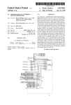
ARCHITECTURE FOR AN I/O PROCESSOR
4,935,894
THAT INTEGRATES A PCI TO PCI BRIDGE
5,353,417 10/1994 Fuoco et al.
5,396,602 3/1995 Amini et al.
395/306
395/293
Inventors: Elliot Garbus, Scottsdale; Peter
573987244
3/1995 Mathews et a1
370/856
5,548,730
8/1996 Young et al. ......................... .. 395/280
sankhagowit, Phoenix; Marc
Goldschmidt, Tempe; Nick Eskandari,
Chandler an of Arm
’
[73] Assignee: Intel Corporation, Santa Clara, Calif.
_
6/1990 Gernes et al. ........................ .. 395/309
_
Primary Examzner—Alpesh M. Shah
Attorney, Agent, or Firm—Blakely, Sokoloff, Taylor &
Zafman
[57]
ABSTRACT
[21] Appl. No.: 870,141
_
[22]
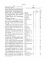
Amulti-functional device that integrates a high performance
Flled:
Jun- 5’ 1997
processor into a PCI to PCI bus bridge. The invention
_
_
consolidates a high performance processor, a PCI to PCI bus
Related U‘S‘ Apphcatlon Data
[63]
Commuanon of Ser' No' 49O’654’ Jun’ 15’ 1995’ abandoned‘
Int. Cl.6 .................................................... .. G06F 13/00
[51]
[52]
[58]
bridge, PCI bus-processor address translation unit, direct
memory acces’s (DMA) controller, memory controller, sec
ondary PCI bus arbitration unit, inter-integrated circuit (IZC)
bus interface unit, advanced programmable interrupt (APIC)
bus interface unit, and a messaging unit into a single system
US. Cl. ...................... .. 395/200.8; 395/309; 370/402
Field Of Search ................................... .. 395/287, 306,
Which utililes a local memory The PCI bus is an industry
395/309, 726, 733, 80001, 856, 2008,
standard high performance, loW latency system bus. The PCI
20083; 370/257, 351, 401, 402; 340/8255
to PCI bridge provides a connection path betWeen tWo
independent 32-bit PCI buses and provides the ability to
[56]
References Cited
overcome PCI electrical loading limits. The addition of the
local processor brings intelligence to the PCI bus bridge.
U.S. PATENT DOCUMENTS
4,935,868
6/1990 Dulac .................................... .. 395/290
26 Claims, 10 Drawing Sheets
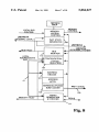
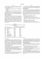
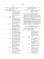
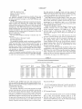
LOCAL
\
MEMORY
33
_
PRocEssoR1
MEMORY
/ 17
l/O
CONTROLLER
PRocEssoR 2
NETWORK
19\
\
21
PRocEssoR/
INTERFACE
PRocEssoR a
pm
PRocEssoR 4
BUS
PCI
PCl-TO-PCI
BR'DGE
—
3C3]
-
SCSI
—
SCSI
Bus
)1
HOST
25
MEMORY
11
\
27
31
\
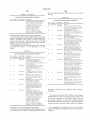
U.S. Patent
Mar. 16, 1999
Sheet 1 0f 10
PRIOR ART
PROCESSOR 1
PROCESSOR 2
17
N ETWORK
l/O
19
/
5,884,027
\
SCSI
PROCEssoR 3
PR‘
PCl-TO-PCI
SEC
PC‘
BRIDGE
58g
PROCESSOR 4
BUS
SCSI
25
HOST
\
MEMORY
13
11
\
_
Flg. 1
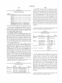
SCSI
27
LOCAL
\
MEMORY
33
NETWORK
PR
E
MEMORY
R1
0C 880
/ 17
{/0
CONTROLLER
PROCEssOR 2
19\
PROCEssOR/
INTERFACE
PROCESSOR a
PR‘
PROCEssOR 4
BUS
SCSI
SEC
BR'DGE
Bus
SCSI
25
HOST
MEMORY
\
\
\
11
27
31
Fig. 2
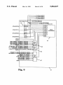
SCSI
U.S. Patent
0000.0000I
Mar. 16, 1999
5,884,027
Sheet 3 0f 10
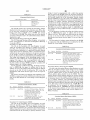
SECONDARY PCI
PRIMARY PCI
ADDRESS SPACE
0000 OOOOH ADDRESS SPACE
4
TRANSACTIONS FORWARDED
UPSTREAM TO THE
PRIMARY PCI BUS
VALID PRIMARY
PCI ADDRESSES
4
—>
VALID SECONDARY Tmg‘gg?g?g?f?gv?gm VALID SECONDARY.
PC‘ ADDRESSES
SECONDARY PCI BUS
—>
<—
TRANSACTIONS FQRWARDED
UPSTREAM TO THE
PC‘ ADDRESSES
VAL") pmMARY
PCI ADDRESSES
PRIMARY PCI BUS
FFFF.FFFFH
<——
FFFF.FFFFH
SECONDARY PCI ADDRESS
REMAIN ON THE SECONDARY
PCI BUS AND ARE NEVER
FORWARDED UPSTREAM
Fig. 4
U.S. Patent
Mar. 16,1999
Sheet 5 0f 10
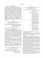
5,884,027
TPT
W
MW
%
W
P R MA R
2m9wo?m z
ml
mm
U
m
m
@W
mm
m
3NPN8ASA8SRmmm
A4 mm
Y5G
Q
/T
w
P
Y
3
N
EUS$52: \m
m.#m6a.9m
mmM05 2
mu
m
B
2\
WP
EN.SB
4'nlv B R DG
SECONDARY PCI BUS
H
ww
.92.054
SECONDARY ADDRESS
TRANSLATION UNIT
/
43b
/
93
M652
R
6V
Fig. 6
U.S. Patent
Mar.
PRIMARY PCI BUS
_
_
_
5,884,027
Sheet 6 0f 10
16,1999
_
_
_
_
_
DMACHANNEL 0
DMACHANNEL 1
____
PCI TO PCI BRIDGE
/
32
SECONDARY PCI BUS
/'
51a
LOCAL BUS
__.__J
DMA CHANNEL 2
/
<1——>
<-———>
V
51b
Fig.
U.S. Patent
Mar. 16,1999
Sheet 7 0f 10
5,884,027
REFRESH
TIMER
LOCAL BUS
coNTRoL
MEMORY
coNTRoL
MEMORY
>
ACCESS
coNTRoL
‘T"
LRDYRCV#
(INTERNAL LOCAL) _'_ _ ’
<
WAIT STATE
GENERATOR
\
109
LRDYFICV# >
¢Bus FAULT
/
LOCAL
ADDRESS/DATA
(ExTEFliqNoAvLngygTEM)
BUS
MONITOR
<
"3
—>coN|=|GuRAT|oN/
BUS _—>
—>
STATUS
REGISTERS
4
107
/
’
ADDRESS
/
DECODE
10‘
'’
ADDRESS
41
LATCH
ADDRESS MULTIPLEXER/
MAI1130] BUS
BURST COUNTER
\
/
105
>
4 MEMORY FAULT
>
103
PARITY
GENERATION
& CHECKER
‘“ '
.
DP[3.0]
111
Fig. 8
U.S. Patent
Mar. 16,1999
Sheet 8 0f 10
5,884,027
"_-——'> P INTA# OUTPUT
_-—> PIINTAII OUTPUT
= P_|NTA# OUTPUT
————> P_INTAII OUTPUT
xINT SELECT BIT
121
P2P PROCESSOR
‘
\
LCCAL PRoCEssoR
.______ OUTBOUND DOORBELLS 0-3
:1
|NTA#/X|NTO#
MU§
= X|NTO#
lNTB#/XINT1#
Au
' X'NT3#
X'Nm
E XINT2#
L‘
——I
INT C#/XINT2#
v1U
lNTD#/X|NT3#
= .Iu
LOCAL
= XINT4# PRoCEssoR
= XINT5#
XINT6#
XINT7#
"‘
> NMI#
/
XINT4#
X|NT5#
34
DMA CHANNELO INTERRUPT PENDING -——I
DMA CHANNEL1 INTERRUPT PENDING —'I X|NT6
DMA CHANNELZ INTERRUPT PENDING ——-0 INT.
DMA CHANNEhBéNTEHRUPT PENDlNG—-——u LATCH
IZC BUS INT. UNIT INTERRuPT PENDING—->
APIC BUS INT. UNIT INTERRLIPT PENDING——> X|NT7
DCCRBELL INTERRuPT PENDING——~ M
5.
\123
PRIMARY ATu/g'mgll DIST INTERRuPT PENDING—> LATCH /
I
PRIMARY PCI BRIDGE INTERFACE EHROH—->
sECoNDARY PCI BRIDGE INTERFACE ERROH-—>
PRIMARY ATu ERR0R——>
sECoNDARY ATu ERROH——-> NM'
LOCAL PRocEssoR ERR0R——> INT
DMA CHANNEL 0 ERR0R——> LATCH
DMA CHANNEL 1 ERR0R—>
DMA CHANNEL 2 ERR0R——~
\
NM|#
Fig. 9
E
127
67
U.S. Patent
Mar. 16, 1999
Sheet 10 0f 10
A
5,884,027
I20 BUS INTERFACE /
61
UNIT
I
2
I
8'5"
_
SHIFT
<—>
SDA
l2C CONTROL REGISTER ....... .. - - ., BUFFER ~ 'REGISTEJ
I CSTATUS REGISTER ~ ------------- a
f
/
,__+ SCL
IZCSLAVEADDRESSREGISTER
------- --
-
-
-*
61a
61¢
I
<——->
MEMORY MAPPED
REGISTERS
\
61b
l2C BUS INTERFACE
INTERRUPT
/
41
4_,
LOCAL
PROCESSOR \
i
LOCAL BUS
Fig. 11
34
5,884,027
1
2
ARCHITECTURE FOR AN I/O PROCESSOR
THAT INTEGRATES A PCI TO PCI BRIDGE
Moreover, the microprocessor or processors in system 11
must typically contend With other bus agents coupled to the
component bus. Such bus contentions typically reduce the
This is a continuation of application Ser. No. 08/489,654
?led Jun. 15, 1995, noW abandoned.
performance of the microprocessor or microprocessors
While performing the input/output functions for the input/
output subsystem.
BACKGROUND OF THE INVENTION
1. Field of the Invention
The present invention pertains to the ?eld of computer
system architecture. More particularly, this invention relates
to an intelligent bus bridge for implementing intelligent
input/output subsystems in computer and server systems.
SUMMARY OF THE INVENTION
10
bus bridge (P2P). Referring noW to FIG. 2, the invention
consolidates a high performance processor, such as an 80960
2. Background
High performance computer systems commonly include
separate input/output subsystems. Such input/output sub
system typically includes a microprocessor that performs
15
input/output functions Which is separate from What may be
such input/output subsystem may perform complex commu
and a messaging unit into a single system 31 Which utiliZes
20
tions for the computer system.
Typically, an input/output subsystem includes a set of
The PCI bus is an industry standard (PCI Local Bus
over a component bus. A processor in such an input/output
Speci?cation, Revision 2.1), high performance, loW latency
25
system bus. The PCI to PCI Bridge provides a connection
path betWeen tWo independent 32-bit PCI buses and pro
vides the ability to overcome PCI electrical loading limits.
The addition of the local processor brings intelligence to the
PCI bus bridge. The local processor and other functional
30
blocks shoWn With dashed box 31 in FIG. 3 illustrate a block
diagram of What Will hereinafter be referred to as the P2P
processor.
The P2P processor is a multi-function PCI device. Func
tion 0 is the PCI to PCI bridge unit. Function 1 is the address
35
translation unit. The P2P processor contains PCI con?gura
tion space accessible through the primary PCI bus.
In the preferred embodiment, the local processor 34 is an
a bus Without interfering With operations by other processors
in the computer system. Such isolation of input/output
transactions on the bus typically enables improved perfor
mance by the main processor or processors in such a
computer system. Such architecture is common in main
frame computer systems Where the processor and the input/
output subsystem is referred to as an I/O channel.
With the advent of computer systems utiliZing
microprocessors, especially server/client systems, the
demand for more poWerful microprocessors has been
increasing to enable more poWerful server/client systems.
This need has been partially met by combining multiple
microprocessors in a single system 11 as shoWn in FIG. 1.
80960 JF processor Which is a member of the Intel i960
Another problem Which exists as more I/O devices are
needed to implement more poWerful server/client systems is
40
that standard component buses that couple input/output
subsystems to other elements of the computer system typi
cally impose electrical loading limitations. Such electrical
loading limitations impose limits on the number of compo
nents coupled to the standard component bus. For example,
45
system component interconnect bus presents only one elec
made visible to the PCI address space
50
In this connection, since some input/output subsystems
require a large number of components that communicate via
55
include a bus bridge circuit 13 that couples the local com
ponent bus 17 to other component buses 19 in the computer
60
access to the local processor local memory 33. The local
processor 34 has direct access to both PCI buses. Address
translation is provided for transactions betWeen the PCI
address space and local processor address space. Address
the components of the input/output subsystem from the other
translation is controlled through programmable registers
component buses. Such a bus bridge circuit enables the
input/output subsystem to contain a large number of com
buses.
processor provides support for local bus arbitration.
Address Translation Units 43a and 43b and Messaging
Unit 45
The address translation unit alloWs PCI transactions direct
system Which connect to a netWork such as a LAN through
ponents required to implement input/output functions While
meeting electrical loading requirements on other component
kept private to the local processor
combination of the tWo.
Local Processor Bus 41
The local processor bus connects to P2P processor I/O
pins to provide bus access to external devices. The P2P
a local component bus Which may exceed the electrical
loading requirements imposed on each connector of a stan
a netWork I/O card 21 or storage devices through SCSI
controllers 23. Such a bus bridge electrically isolates the
microprocessor or microprocessors 25, the memory 27 and
information concerning the local processor needed to prac
tice the invention is provided herein.
The local processor operates out of its oWn 32-bit address
space and not PCI address space. Memory on the local
processor bus can be:
trical load. Such electrical loading limitations ensure that
signal quality on a fully loaded bus is suf?cient for reliable
dard component bus, an input/output subsystem may also
microprocessor family. The 80960 JF processor is imple
mented Without functional modi?cation in the P2P proces
sor. The i960 Jx Microprocessor User’s Manual available
from Intel Corporation provides further details although all
one prior art bus standard requires that each connector on a
operation.
a local memory 33. It is an integrated processor that
addresses the needs of intelligent I/O applications and helps
reduce intelligent I/O system costs.
specialiZed input/output devices coupled for communication
subsystem typically performs the input/output functions via
JF processor available from Intel Corporation (the local
processor), a PCI to PCI bus bridge 32, PCI bus-processor
address translation unit, direct memory access (DMA)
controller, memory controller, secondary PCI bus arbitration
unit, inter-integrated circuit (12C) bus interface unit,
advanced programmable interrupt (APIC) bus interface unit,
referred to as the host or main microprocessor. For example,
nication netWork interface functions or disk control func
The present invention is a multi-functional device that
integrates a high performance processor into a PCI to PCI
65
accessible from both the PCI interface and the local proces
sor Which alloW ?exibility in mapping the tWo address
spaces. A messaging unit 45 provides a mechanism for data
to be transferred betWeen the PCI system and the local
5,884,027
3
4
processor and notifying the respective system of the arrival
every bus master the opportunity to gain control of the local
bus. The algorithm 10 combines a round-robin scheme with
a prioritiZing mechanism.
I2C Bus Interface Unit 61
of new data through an interrupt. The messaging unit can be
used to send and receive messages.
PCI to PCI Bridge Unit 32
The PCI to PCI Bridge Unit connects two independent
PCI buses. The bridge allows certain bus transactions on one
PCI bus to be forwarded to the other PCI bus. It also allows
The I2C (Inter-Integrated Circuit) Bus Interface Unit
allows the local processor to serve as a master and slave
device residing on the 12C bus. The I2C bus is a serial bus
developed by Philips Corporation consisting of a two pin
fully independent PCI bus operation, including independent
interface. The bus allows the P2P processor to interface to
clocks. Dedicated data queues support high performance
other I2C peripherals and microcontrollers for system man
bandwidth on the PCI buses. PCI 64-bit Dual Address Cycle
agement functions. It requires a minimum of hardware for an
(DAC) addressing is supported.
The PCI to PCI bridge has dedicated PCI con?guration
space that is accessible through the primary PCI bus.
The PCI to PCI bridge in the P2P processor is fully
compliant with the PCI to PCI Bridge Architecture
economical system to relay status and reliability information
on the I/O subsystem to an external device.
AZIC Bus Interface Unit 63
The APIC bus interface unit provides an interface to the
15
Speci?cation, Rev. 1.0 published by the PCI Special Interest
(APIC) bus that allows I/O APIC emulation in software.
Group.
Interrupt messages can be sent on the bus and EOI messages
Private PCI Devices
can be received.
The P2P processor, by design, explicitly supports private
Interrupt Routing 67
PCI devices that can use the secondary PCI bus yet avoid
detection by the PCI con?guration software. The PCI to PCI
bridge 32 and the secondary address translation unit 43b
work together to hide private devices from PCI con?gura
tion cycles and to allow these devices to utiliZe a private PCI
address space. These devices can be con?gured by the
secondary address translation unit through normal PCI con
Four PCI interrupt inputs are provided which can be
routed to either local processor interrupt inputs or to PCI
Interrupt output pins.
TERMINOLOGY AND CONVENTIONS
25
Integrated Memory Controller 47
“nnnH”, where the “H” signi?es hexadecimal. Binary num
The integrated memory controller provides direct control
for external memory systems. Support is provided for
bers are shown with the subscript 2.
Fields
A preserved ?eld in a data structure is one that the
processor does not use. Preserved ?elds can be used by
DRAM, SRAM, ROM, and Flash Memory. The integrated
memory controller provides a direct connect interface to
memory 33 that usually does not require external logic. It
features programmable chip selects, a wait state generator,
software; the processor will not modify such ?elds.
35
The external memory can be con?gured as PCI address
able memory or as private local processor memory.
DMA Controller 51a and 51b
The DMA Controller allows low-latency, high-throughput
data transfers between PCI bus agents and local memory.
There are three separate DMA channels to accommodate
data transfers. Two channels are dedicated to primary PCI
bus data transfers and one channel is dedicated to secondary
PCI bus data transfers. The DMA Controller supports chain
ing and unaligned data transfers. It is programmable only
condition.
45
programmable priorities is implemented. Six PCI Request
A read/clear ?eld can also be read to return the current
value. A write to a read/clear ?eld with the data value of 0
will cause no change to the ?eld. Awrite to a read/clear ?eld
with a data value of 1 will cause the ?eld to be cleared (reset
to the value of 0). For example, if a read/clear ?eld has a
value of FOH, and a data value of 55H is written, the
resultant ?eld will be AOH.
Terminology
and Grant signal pairs are provided. The arbitration unit may
device, namely the primary internal PCI arbitration unit 55a
which arbitrates for the primary bridge interface, the primary
ATU, DMA Channel 0, and DMA Channel 1. The secondary
A reserved ?eld is a ?eld that may be used by an
implementation. If the initial value of a reserved ?eld is
supplied by software, this value must be Zero. Software
should not modify reserved ?elds or depend on any values
in reserved ?elds.
A read only ?eld can be read to return the current value.
Writes to read only ?elds are treated as no-op operations and
will not change the current value nor result in an error
through the local processor 34.
Secondary PCI Arbitration Unit 53
The Secondary PCI Arbitration Unit provides PCI arbi
tration for the secondary PCI Bus. A fairness algorithm with
be disabled to allow for external arbitration.
Internal PCI and Local Bus Arbitration Units 55a, 55b and
57
The P2P processor contains two internal arbitration units
which control access to the internal PCI buses within the
Representing Numbers
All numbers set forth herein are base 10 unless designated
otherwise. In text, numbers in base 16 are represented as
?guration cycles.
and byte parity.
three-wire Advanced Programmable Interrupt Controller
To aid the discussion of the P2P architecture, the follow
ing terminology is used:
55
Downstream
At or toward a PCI bus with a higher number
DWORD
Host processor
32-bit data word
Processor located upstream from the P2P
processor
Local processor bus
(after con?guration)
internal PCI arbitration unit 55b arbitrates for the secondary
Local bus
Local memory
bridge interface, the secondary ATU, and DMA Channel 2.
Upstream
Each internal PCI arbitration unit uses a ?xed round-robin
Memory subsystem on the local bus
At or toward a PCI bus with a lower number
(after con?guration)
arbitration scheme with each device on a bus having equal
priority.
The P2P processor also requires an arbitration mechanism
to control local bus ownership. The local bus arbitration unit
(LBAU) 57 implements a fairness algorithm which allows
BRIEF DESCRIPTION OF THE DRAWINGS
FIG. 1 is a block diagram showing a system using a prior
art PCI to PCI bridge.
5,884,027
5
6
FIG. 2 is a block diagram showing a system using the
invented PCI to PCI bridge With processor according to the
present invention.
FIG. 3 is a block diagram shoWing the invented P2P
cessor bus. The address, hoWever, Will not increment for
bursts longer than 4 Words. This implies that memory
controllers on the local bus must increment the address for
each access in a burst.
PCI TO PCI Bridge Unit
OvervieW
processor.
FIG. 4 shoWs the directions in Which transactions ?oW
betWeen the primary and secondary address spaces of the
PCI to PCI bridge.
FIG. 5 is a block diagram of the PCI to PCI bridge.
10
FIG. 6 is a block diagram of the primary and secondary
archy is electrically a separate entity but Where all buses
ATUs.
Within the hierarchy are logically one bus. The PCI to PCI
bridge unit does not increase the bandWidth of a PCI bus, it
FIG. 7 is a block diagram shoWing the connections of the
DMA controllers to the various buses.
FIG. 8 is a block diagram of the memory controller.
FIG. 9 is a block diagram shoWing the connections
betWeen the local processor and the PPIC.
FIG. 10 is a block diagram shoWing the connections of the
internal PCI arbitration units.
FIG. 11 is a block diagram of the 12C Bus Interface Unit
and its interface to the local bus.
DETAILED DESCRIPTION OF THE
INVENTION
15
The PCI to PCI bridge unit provides:
Independent 32-bit primary and secondary PCI buses With
support for concurrent operations in either direction;
20
25
35
40
A PCI to PCI bridge is programmed With a contiguous
range of addresses Within the memory and I/O address
spaces, Which then become the secondary PCI address
45
space. Any address present on the primary side of the bridge
Which falls Within the programmed secondary space is
forWarded from the primary to the secondary side While
addresses outside the secondary space are ignored by the
bridge. The secondary side of the bridge Works in reverse of
the primary side, ignoring any addresses Within the pro
grammed secondary address space and forWarding any
50
devices. APCI transaction initiated on one side of the bridge
Will address the initiating bus bridge interface as a target and
55
made that impact the 80960 JF processor as used in the P2P
processor.
PCI devices on either side.
The PCI to PCI bridge unit of the P2P processor adheres,
at a minimum, to the required features found in the PCI to
60
PCI Bridge Architecture Speci?cation Revision 1.0 and the
PCI Local Bus Speci?cation Revision 2.1. The folloWing is
a description of the bridge functionality and Will refer to the
PCI to PCI Bridge and PCI Bus Speci?cations Where
65
Architectural Description
register must have the Bus Width bits set to 102 indicating
a 32-bit Wide bus.
appropriate.
Bus
masters on the local bus other than the local processor are
alloWed to have unlimited burst lengths on the local pro
the transaction Will be completed by the target bus interface
operating as a master device. The bridge is transparent to
Memory Regions
To achieve optimal performance from DMA accesses, bus
addresses outside the secondary space to the primary side as
shoWn in FIG. 4.
The primary and secondary interfaces of the PCI bridge
each implement PCI 2.1 compliant master and target
TWo 32-bit Timers
Differences
Because the P2P processor Peripheral Memory-Mapped
Registers are 32-bits Wide, Memory Region 0 and 1 must be
designated a 32-bit region. Therefore, the PMCONOi1
the primary and the secondary PCI buses. PCI supports three
separate address spaces:
Four Gbyte memory address space
64 Kbyte I/O address space (With 16-bit addressing)
Separate con?guration space
Thirty-tWo 32-bit integer registers
The folloWing is a description of system design decisions
Special mode of operation that alloWs for positive decod
ing on the primary and secondary interfaces.
The bridge unit operates as an address ?lter unit betWeen
High performance instruction execution core
4-Kbyte 2-Way set associative instruction cache
Programmable bus controller
1-Local register Data RAM
Local register cache, providing storage for up to 8 local
register sets
Advanced interrupt controller
on the secondary bus;
64-bit addressing mode from the secondary PCI interface;
Private device con?guration and address space for private
Theory Of Operation
folloWs:
2-Kbyte direct mapped data cache
VGA palette snooping and VGA compatible addressing
PCI devices on the secondary PCI bus;
30
describes hoW the 80960 JF processor is con?gured or
for more details about the 80960 JF processor.
Features
The basic features of the 80960 JF processor are as
Separate memory and I/O address spaces on the second
ary side of the bridge;
TWo 64 byte posting buffers for both upstream and
doWnstream transactions;
The folloWing is a description of the 80960 JF micropro
otherWise different from the description of the part in the
i960 JX Microprocessor User’s Manual.
OvervieW
The 80960 JF processor is implemented Without func
tional changes in the P2P processor, ie no internal logic is
altered. Refer to the i960 JX Microprocessor User’s Manual
only alloWs that bus to be eXtended for applications requir
ing more I/O components than PCI electrical speci?cations
alloW.
The invention Will noW be described in terms of its
functional blocks as set forth in FIG. 3.
Local Processor
cessor used as the local processor in the P2P processor. It
The PCI to PCI bridge unit 32 is a device that alloWs the
extension of a PCI Bus beyond its limited physical con
straint of 10 electrical PCI loads. The bridge unit uses the
concept of hierarchical busses Where each bus in the hier
The PCI to PCI bridge unit can be logically separated into
four major components as folloWs:
5,884,027
8
Primary PCI Interface
Secondary PCI Interface
the opposite side of the bridge, the PCI to PCI bridge unit
implements tWo 64 byte posting buffers 77 and 79. The
bridge supports both Delayed and Posted transactions.
In a Delayed transaction, the information required to
complete the transaction is latched and the transaction is
terminated With a Retry. The bridge then performs the
Posting Buffers
Con?guration Registers
The block diagram of the bridge in FIG. 5 shoWs these
major functional units.
Primary PCI Interface
transaction on behalf of the initiator. The initiator is required
to repeat the original transaction that Was terminated With a
The primary PCI interface 71 of the PCI to PCI bridge
unit can act either as a target or an initiator of a PCI bus
transaction. For most systems, the primary interface Will be
connected to the PCI side of a Host/PCI bridge Which is
typically the loWest numbered PCI bus in a system hierar
chy. The primary interface consists of the mandatory 50
signal pins de?ned Within the PCI to PCI Bridge Architec
ture Speci?cation Revision 1.0 and four optional interrupt
p1ns.
Retry in order to complete the transaction.
10
target bus.
15
The primary PCI interface implements both an initiator
(master) and a target (slave) PCI device. When a transaction
is initiated on the secondary bus, the primary master state
machine, Which is described in the PCI Local Bus Speci?
cation Revision 2.1, completes the transaction (Write or
read) as if it Was the initiating device. The primary PCI
Delayed and Posted transactions are discussed in detail
beloW.
The bridge uses tWo posting buffers:
doWnstream posting buffer 77 for data ?oWing from the
primary interface to the secondary interface
upstream posting buffer 79 for data ?oWing from the
secondary interface to the primary interface
Each buffer has associated address/control registers to
maintain information about the transaction.
interface, as a PCI target for transactions that need to
complete on the secondary bus, accepts the transaction and
forWard the request to the secondary side. As a target, the
primary PCI interface uses positive decoding to claim the
PCI transaction addressed beloW the bridge and then for
Ward the transaction onto the secondary master interface.
In a Posted transaction, the transaction is alloWed to
complete on the initiating bus before completing on the
Con?guration Registers
25
Every PCI device implements a separate con?guration
address space and con?guration registers 81. The ?rst 16
The primary PCI interface is responsible for all PCI
command interpretation, address decoding and error han
bytes of the bridge con?guration header format implement
the common con?guration registers required by all PCI
devices. The value in the read-only Header Type Register
dling.
de?nes the format for the remaining 48 bytes Within the
PCI con?guration for the primary and secondary
header and returns a 01H for a PCI to PCI bridge.
Devices on the primary bus can only access the PCI to
interfaces, interrupt routing logic (described beloW), sec
ondary PCI bus arbitration (described beloW) is completed
through the primary interface. Con?guration space registers
support these functions.
Secondary PCI Interface
The secondary PCI interface 73 of the PCI to PCI bridge
PCI bridge con?guration space With Type 0 con?guration
commands. Devices on the secondary PCI bus can not
35
access bridge con?guration space With PCI con?guration
cycles. The con?guration registers hold all the necessary
address decode, error condition and status information for
unit functions in almost the same manner as the primary
interface. It includes both a PCI master and a PCI slave
device and implements the “second” PCI bus With a neW set
both sides of the bridge.
Address Decoding
of PCI electrical loads for use by the system. The secondary
PCI interface consists of the mandatory 49 pins. SiRST# is
The P2P processor provides three separate address ranges
Warding them up the bridge to the master on the primary
side. As a master (initiator), the secondary PCI interface is
responsible for completing transactions initiated on the
primary side of the bridge. The secondary PCI interface uses
limit register to implement an address range. The address
ranges are positively decoded on the primary interface With
any address Within the range considered a secondary address
that are used to determine Which memory and I/O addresses
are forWarded in either direction across the bridge portion of
an output instead of an input on the secondary side.
the P2P processor. There are tWo address ranges provided for
As a slave (target), the secondary PCI interface is respon
memory transactions and one address range provided for I/O
sible for claiming PCI transactions that do not ?t Within the
bridge’s secondary memory or I/O address space and for 45 transactions. The bridge uses a base address register and
and therefore capable of being forWarded doWnstream
across the bridge. On the secondary interface, the address
inverse decoding of the bridge address registers and only
forWards addresses Within the primary address space across
ranges are inversely decoded. This means that any address
the bridge.
The secondary PCI interface also implements a separate
address space for private PCI devices on the secondary bus
Where it ignores and does not forWard a range of primary
addresses de?ned at con?guration time by the local proces
outside the programmed address ranges is capable of being
forWarded upstream through the bridge.
Standard bridge unit address decoding can also be modi
55
sor.
the secondary bridge interface and disable the basic inverse
address decoding used by PCI to PCI bridges.
I/O Address Space
As a special mode of operation, the secondary PCI
interface performs positive address decoding based upon its
oWn set of memory and I/O address registers. This mode of
operation is enabled through the Secondary Decode Enable
Register (SDER) and has a side effect of disabling the
inverse decoding of the standard bridge address registers on
the secondary interface.
Posting Buffers
To hide the latency incurred in the arbitration and acqui
sition of a PCI target during read and Write transactions to
?ed by the Secondary Decode Enable Register (SDER). The
bits Within this register enable positive address decoding by
The PCI to PCI bridge unit implements one program
mable address range for PCI I/O transactions. A continuous
I/O address space is de?ned by the I/O Base Register
(IOBR) and the I/O Limit Register (IOLR) in the bridge
con?guration space. The upper four bits of the IOBR cor
65
respond to AD[15:12] of the I/O address and the loWer
tWelve bits are alWays OOOH forcing a 4 Kbyte alignment for
the I/O address space. The upper four bits if the IOLR also
5,884,027
9
10
correspond to AD[15:12] and the lower twelve bits are
will always use the same PCI command type on the sec
FFFH forcing a granularity of 4 Kbytes.
The bridge unit will forward from the primary to second
ondary bus that was claimed by the primary slave interface
on the primary bus (except for certain cases during Memory
Write and Invalidate). All dual address cycles (PCI transac
tions with 64-bit address) are always claimed by the sec
ary interface an I/ O transaction that has an address within the
address range de?ned (inclusively) by the IOBR and the
ondary interface.
IOLR. In this instance the primary interface acts as a PCI
target and the secondary interface acts as a PCI initiator for
Any PCI memory transaction present on the secondary
bus that falls outside the address range de?ned by the two
the bridged I/O transaction.
register pairs (MBR-MLR and PMBR-PMLR) will be for
If an I/O read or write transaction is present on the
secondary bus, the bridge unit forwards it to the primary
10
interface if the address is outside the address range de?ned
by IOBR and IOLR. In this instance the secondary interface
bus. Dual address cycles are constrained to the upper 4
acts as a PCI target and the primary interface serves as a PCI
Gbytes of the 64-bit address space.
initiator.
The P2P processor only supports 16-bit addresses for I/O
15
transactions and therefore any I/O transaction with an
address greater than 64 Kbytes will not be forwarded over
either interface. The bridge assumes AD[31116] =0000H
even though these bits are not implemented in the IOBR and
the IOLR. The bridge unit must still perform a full 32-bit
decode during an I/O transaction to check for AD[31116]
=0000H per the PCI Local Bus Speci?cation.
ISA Mode
The PCI to PCI bridge unit of the P2P device implements
an ISA Mode bit in the Bridge Control Register (BCR) to
provide ISA-awareness for ISA I/O cards on subordinate
PCI buses. ISA Mode only affects I/O addresses within the
address range de?ned by the IOBR and IOLR registers.
The bridge response to memory transactions on either
interface may be modi?ed by the following register bits
from the bridge con?guration space:
Master Enable bit in the Primary Command Register
(PCMD)
Memory Enable bit in the Primary Command Register
(PCMD)
VGA Enable bit in the Bridge Control Register (BCR)
Secondary Positive Memory Decode Enable bit in the
Secondary Decode Enable Register (SDER)
25
The Secondary Positive Memory Decode Enable bit in the
SDER modi?es secondary address decoding. It enables an
address range register pair, Secondary Memory Base Reg
ister (SMBR) and Secondary Memory Limit Register
When ISA Mode is enabled by setting the ISA Mode bit, the
(SMLR), that de?ne an address window for claiming
memory transactions on the secondary bus and forwarding
bridge will ?lter out and not forward I/O transactions with
through the bridge. The decoding and transaction claiming
addresses in the upper 768 bytes (300H) of each naturally
aligned 1 Kbyte block. Conversely, I/O transactions on the
secondary bus will inversely decode the ISA addresses and
works in the same manner as positive decoding on the
primary bus for the MBR/MLR and PMBR/PMLR address
pairs. The Secondary Positive Memory Decode Enable bit
therefore forward I/O transactions with addresses in the
upper 768 bytes of each naturally aligned 1 Kbyte block.
warded upstream across the bridge from the secondary to
primary interface. The secondary interface will forward all
dual address cycles from the secondary bus to the primary
35
Memory Address Space
The PCI to PCI bridge unit supports two separate address
ranges for forwarding memory accesses downstream from
also disables the inverse decoding performed on the sec
ondary interface that claims memory transactions with
addresses outside the MBR/MLR and PMBR/PMLR
address ranges. Inverse decoding is never performed on the
primary interface on behalf of the MBR/MLR and PMBR/
the primary to secondary interfaces. The Memory Base
Register (MBR) and the Memory Limit Register (MLR)
PMLR address pairs.
64-Bit Address Decoding-Dual Address Cycles
The bridge unit supports the dual address cycle command
de?ne one address range and the Prefetchable Memory Base
Register (PMBR) and the Prefetchable Limit Register
(PMLR) de?ne the other address range. The prefetchable
for 64-bit addressing on the secondary interface of the
address range is used in determining which memory spaces
are capable of prefetching without side effects. Both register
bridge unit only. Dual address cycles allow 64-bit addressing
Memory Read Line, Memory Read Multiple, Memory
by using two PCI address phases; the ?rst one for the lower
32 bits and the second one for the higher 32 bits.
The bridge unit typically decodes and forwards all dual
Write, and Memory Write and Invalidate transactions across
the bridge. In the case where the two register pairs overlap,
address cycles from the secondary to the primary interface
regardless of the address ranges de?ned in the MBR/MLR
45
pairs determine when the bridge will forward Memory Read,
one address range results that is the summation of both
and PMBR/PMLR register pairs. Dual address cycles will
registers combined with the prefetchable range having pri
not be forwarded if the Secondary Subtractive Decoding
ority over bridge read transaction response.
The upper twelve bits of the MBR, MLR, PMBR, PMLR
registers correspond to address bits AD[31120] of a primary
Enable bit in the SDER is set.
or a secondary memory address. For decoding purposes, the
The bridge unit will use Subtractive Decode timing (assert
55
bridge assumes that AD[1910] of both memory base registers
are OOOOOH and that AD[1910] of both memory limit regis
DEVSEL# on the ?fth clock after FRAME# is asserted) for
claiming dual address cycles. This allows other agents on the
secondary PCI bus to claim dual address cycles before the
bridge unit.
The primary interface will not forward dual address
ters are FFFFFH. This forces the memory address ranges
supported by the bridge unit to be aligned on 1 Mbyte
cycles.
boundaries and to have a siZe granularity of 1 Mbyte. The
lower four bits in all four registers are read only and return
32 bits of a 64-bit address is the addition of 32-bit address
The mechanism for holding and forwarding the high order
Zero when read.
registers associated with the secondary to primary data path.
Any PCI memory transaction (not I/O) present on the
primary bus that falls inside the address ranges de?ned by
These registers will store the high order 32 bits of a 64-bit
the two register pairs (MBR-MLR and PMBR-PMLR) will
be forwarded downstream across the bridge from the pri
mary to secondary interface. The secondary master interface
address that is transmitted during the second address phase
65
of a dual address cycle. In addition, the master and slave
state machines must be able to support the dual address cycle
and the DAC command.
5,884,027
11
12
The secondary PCI interface must adhere to the de?nition
The response to DAC cycles on the secondary interface
may be modi?ed by the following register bits from the
of a PCI master and slave device as de?ned within the PCI
bridge con?guration space:
Local Bus Speci?cation and the PCI to PCI Bridge Archi
tecture Speci?cation.
the Master Enable bit in the Primary Command Register
Posting Buffers
(PCMD)
The PCI to PCI bridge unit has two posting buffers that
are used for both Delayed transactions and Posted transac
the Memory Enable bit in the Primary Command Register
(PCMD)
The Memory Enable bit in the PCMD register must be set
to allow the bridge to enable the bridge to respond to any
kind of memory cycle, 32 or 64 bit. The Master Enable bit
in the PCMD must be set to allow the primary interface to
master PCI transactions.
BRIDGE OPERATION
The bridge unit of the P2P processor is capable of
forwarding all types of memory, I/O and con?guration
15
tions. The downstream posting buffer 77 is in the data path
from the primary interface to the secondary interface. The
upstream posting buffer 79 is in the data path from the
secondary interface to the primary interface. FIG. 5 shows
the two posting buffers between the primary and secondary
interfaces.
The downstream posting buffer is used by:
Posted Writes from the primary bus
Delayed Write Requests from the primary bus
Delayed Read Completions returning to the secondary bus
Delayed Write Completions returning to the secondary
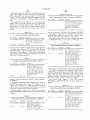
commands from one PCI interface to the other PCI interface.
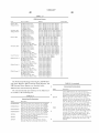
Table 1 de?nes the PCI commands supported and not
supported by the PCI to PCI bridge unit and its two PCI
bus
interfaces. PCI commands are encoded within the C/BE
[3:0]# pins on either interface. To prevent deadlock due to
The upstream posting buffer is used by:
two different interfaces, the bridge gives priority to the
Posted Writes from the secondary bus
primary interface when transactions occur on both interfaces
Delayed Write Requests from the secondary bus
Delayed Read Completions returning to the primary bus
simultaneously.
TABLE 1
PCI Commands
C/BE # PCI Command
Initiator: Primary Bus Initiator: Secondary Bus
Target: Secondary Bus Target: Primary Bus
OOOO2
00012
Ignore
Ignore
Ignore
Ignore
Forward
Interrupt Acknowledge
Special Cycle
00102
I/O Read
Forward
00112
I/O Write
Forward
Forward
01002
01012
Reserved
Reserved
Ignore
Ignore
Ignore
Ignore
01102
01112
Memory Read
Memory Write
Forward
Forward
Forward
Forward
10002
10012
Reserved
Reserved
Ignore
Ignore
Ignore
Ignore
10102
10112
11002
11012
11102
11112
Con?guration Read
Con?guration Write
Memory Read Multiple
Dual Address Cycle
Memory Read Line
Memory Write and Invalidate
Forward
Forward
Forward
Ignore
Forward
Forward
Forward
Forward
Forward
Forward
Forward
Forward
Delayed Write Completions returning to the primary bus
PCI Interfaces
The P2P bridge unit has a primary PCI interface and a
secondary PCI interface. When transactions are initiated on
Write posting allows the bridge to achieve its full band
the primary bus and claimed by the bridge, the primary
width potential while hiding the latency associated with
traveling through the bridge and the latency associated with
interface serves as a PCI target device and the secondary
interface serves as an initiating device for the true PCI target
be used simultaneously.
acquiring the target bus. The two sets of posting buffers can
Posting Buffer OrganiZation
on the secondary bus. The primary bus is the initiating bus
and the secondary bus is the target bus. The sequence is
Each posting buffer can hold 64 bytes of data organiZed
in 16 entries of 4 bytes each (16 DWORDs). Each buffer can
reversed for transactions initiated on the secondary bus. The
interfaces are de?ned below.
55
Primary Interface
The primary PCI interface 71 of the bridge unit is the
interface connected to the lower numbered PCI bus between
the two PCI buses that the P2P device bridges.
The primary PCI interface must adhere to the de?nition of
a PCI master and slave device as de?ned within the PCI
Local Bus Speci?cation and the PCI to PCI Bridge Archi
tecture Speci?cation.
outside of the posting buffer.
The internal addressing of the posting buffers is in a
Secondary Interface
The secondary PCI interface 73 of the bridge unit is the
interface connected to the higher numbered PCI bus between
the two PCI buses that the P2P device bridges.
hold:
One Posted Write transaction of up to 64 bytes or
One Delayed Completion transaction up to 64 bytes or
One Delayed Write transaction up to 4 bytes
Associated with each posting buffer is an address register
and a set of tag bits and valid bits.
The bridge can also store one Delayed Read Request
circular fashion such that when a transaction enters an empty
65
buffer, it will be immediately forwarded to the top. No PCI
clocks are required to move data from one entry in the buffer
to the neXt.
5,884,027
14
13
Posting Buffer Operation
This allows certain con?guration registers to be initialiZed
Both posting buffers are used to help the bridge achieve
before PCI con?guration begins.
the full PCI bandwidth and to hide the latency of acquiring
The local processor reads and writes the bridge con?gu
two PCI buses for every transaction crossing the bridge. The
ration space as memory-mapped registers. Table 3 shows the
Posting Disable bit in the EBCR register must be Clear I0 5 register and its associated offset used in a PCI con?guration
allOW the buffers I0 POSI IfaIlSaCIlOIlScommand and its memory-mapped address in the local
The nature of the posting buffers allows for concurrent
processor address space,
Operatlohs froth the prhhaty t0 seeoheary PCI lhtertaees ahd
The assertion of the PiRST# signal on the primary side
froth the seeohdary t0 Pnthahy PCI lhterfaees- Thls theahs
of the bridge affects the state of most of the registers
that trahsaetlohs t0 Opposlte lhterfaees may occur 0h both 10 contained within the bridge con?guration space. Unless
Pct lhtehfaees at the samethhe- From the thotheht a trahs'
aetloh 1S lhltlateh t0 the hhdge, the target lhterfeee attempts
t0_ga_1h thastershlp of the target hhs- The theehahlsth used for
this is the standard PCI arbitration mechanism used on the
otherwise noted, all bits and registers will return to their
stated default state value upon primary reset. The reset state
of the secondary SiRST# output does not affect the state of
the registers unless explicitly noted
primary and the secondary interfaces.
15
As a default reset state, the posting buffers will be marked
invalid. Any subsequent PCI reset event will force all the
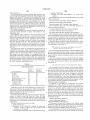
TABLE 3
buffers to be Cleared by being marked invalid~
PCI to PCI Bridge Con?guration Register Addresses
Transaction Ordering Rules
Because
the
brid g e can rocess multi
le transactions
it 20
'
~
'
p
' ' >
must maintain proper ordering to avoid deadlock conditions
and improve throughput. Table 2 contains the ordering rules
for multiple transactions. The ?rst row contains the trans
action that has been accepted. The ?rst column is the
_
Slze
in
Register Name
d
_
Address
Bytes Offset
5
ggg
Primary Command Register _ PCMDR
transaction that was just latched. The table indicates whether 25 Primary Status Register - PSR
the new transaction can pass the previous accepted transacRevlslen ID Reglster ' RIDR
2
2
1
04H
06H
08H
tion (denoted as Yes) the new transaction can not
3
_
’
_
[lg
ass the
p
Egg
Class Code Reglster ' CCR
_
09H
Cacheline Size Register — CLSR
1
OCH
previous accepted transaction (No), or the new transaction
Primary Latency Timer Register _ PLTR
1
ODH
should not be accepted (Do Not Accept). Transactions not
Header Type Register - HI‘R
1
OEH
accepted should be signaled a Retry.
TABLE 2
Transaction Passing
Pass accepted Pass accepted
Posted Memory Delayed Read
Pass accepted
Delayed Write
Pass accepted
Delayed Read
Pass accepted
Delayed Write
Write?
Request?
Request?
Completion?
Completion?
New Posted Memory Write
No
Yes
Yes
Yes
Yes
New
New
New
New
No
No
No
Yes
Do Not Accept
Do Not Accept
Yes
Yes
Do Not Accept
Do Not Accept
Yes
Yes
No
No
Do Not Accept
No
Yes
Yes
Do Not Accept
Do Not Accept
Pass?
Delayed
Delayed
Delayed
Delayed
Read Request
Write Request
Read Completion
Write Completion
Register De?nitions
.
.
.
45
The PCI to PCI bridge con?guration registers are
described below. The con?guration space consists of 8, 16,
TABLE 3_continued
24, and 32-bit registers arranged in a prede?ned format. The
PCI to PCI Bridge Con?guration Register Addresses
con?guration registers are accessed through Type 0 Con?guration Reads and Writes on the primary side of the bridge 50
and through local processor local operations.
Register Name
Each register other than those de?ned by the PCI Local
Bus Speci?cation and the PCI to PCI Bridge Architecture
'
'
'
'
'
'
'
S_
mm Address
Bytes Offset
ghmagy Bu; NulilnbelRelglster ' PBSI‘IIiIR
€COI1
ary
11S
um
6T
with an active IDSEL or a memory-mapped local processor
-
-
-
-
1
1g:
1
1
1
lAH
1EH
1CH
egister -
Speci?cation is detailed in functionality, access type (read/
Subordinate Bus Number Register _ SubBNR
write, read/clear, read only) and reset default condition. As 55 Secondary Latency Timer Register _ SLTR
stated, a Type 0 con?guration command on the primary side
I/O Base Register - IOBR
I/O Llmlt heglster - IQLR
1
1DH
Secondary Status Register — SSR
2
1EH
Memory Base Register _ MBR
2
20H
for the registers with offsets up to 3EH are de?ned with the
Memory Limit Register _ MLR
PCI to PCI Bridge Architecture Speci?cation Rev. 1.0, and 60 Prefetchable Memory Base Register - PMBR
therefore, are not detailed herein. Registers with offsets
Prefetchable Memory Limit Register - PMLR
2
2
2
22H
24H
26H
greater than 3EH are implementation speci?c to the P2P
Budge C°ntr_°1Reg1Ster ' BC?
2
3EH
Extended Bridge Control Register — EBCR
Secondary IDSEL Select Register — SISR
2
2
40H
42H
An a ltlona requlrément exlsts to_ a OW t e Oca proPrimary Bridge Interrupt Status Register — PBISR
cessor to access the bridge con?guration space. Some reg- 65 Secondary Bridge Interrupt Status Register _ SBISR
4
4
44H
48H
isters that are read only from Type 0 Con?guration Read and
4
4CH
access is required to read or write these registers. The format
rocessor
p
.
1
.
.
11
h
1
1
Write commands may be writable from the local processor.
Secondary Arbitration Control Register - SACR
5,884,027
15
16
TABLE 3-continued
TABLE 4a-continued
PCI to PCI Bridge Con?guration Register Addresses
Extended Bridge Control Register — EBCR
Size
in
Bit
Default
Read/Write
Description
02
O2
Read/Write
Reset Bridge — When the bit
is set, the entire PCI to PCI
Address
Register Name
Bytes Offset
PCI Interrupt Routing Select Register — PIRSR
Secondary I/O Base Register — SIOBR
Secondary I/O Limit Register — SIOLR
Secondary Memory Base Register — SMBR
Secondary Memory Limit Register — SMLR
Secondary Decode Enable Register — SDER
4
1
1
2
2
2
50H
54H
55H
58H
5AH
5CH
bridge Will be reset. All
registers of the bridge Will
be set to their default values
1O
(except for secondary bus
reset bit of the BCR), all
state machines Will be reset
and all buffers Will be
cleared. The secondary
As previously noted, the bits in the Vendor ID Register
through the Bridge Control Register-BCR adhere to the
de?nitions in the PCI Local Bus Speci?cation, and, therefore
reset bit in the BCR Will be
set in insure minimum PCI
reset time. SoftWare Will
15
be required to clear this bit
to deassert the secondary
need not be described herein. The following is a description
of the registers added to the PCI Local Bus Speci?cation to
bus reset.
O1
implement the PCI to PCI bridge according to the present
invention. The added registers begin at an address offset of
Varies With
Read/Write
external state
Processor Reset- This bit
Will reset the local
40H as shoWn in Table 3.
of RSTLMODE
processor only Without
pin at primary
Extended Bridge Control Register-EBCR
PCI bus reset
resetting the secondary side
of the bridge. Setting this
The Extended Bridge Control Register is used to control
the extended functionality the bridge implements over the
base PCI to PCI Bridge Architecture Speci?cation. It has
enable/disable bits for the extended functionality of the
bit Will place the processor
into a reset state and keep it
25
there. SoftWare Will be
required to clear this bit to
deassert local processor
reset.
bridge.
The default condition for
this bit is based on the
external state of the
TABLE 4a
RSTLMODE pin at
the rising edge of PiRST#.
Extended Bridge Control Register — EBCR
If the external state of the
Bit
Default
Read/W rite
Description
15:07 0000000002
Read Only
Reserved
06
Read/W rite
pin is high, the bit is set.
If the external state of the
Varies With
external state
Con?guration Cycle
pin is loW, the bit is
35
cleared.
O0
Disable — When this bit is
O2
Read/Write
set, the primary PCI inter
of CONFIGLMODE
Posting Disable — If this bit
is set, the bridge is not
alloWed to post Write
transactions from either
bridge interface. All trans
pin at primary
face of the P2P Processor
PCI bus reset
Will respond to all
con?guration cycles With a
Retry condition. When
clear, the P2P Processor
Will respond to the
Delayed transactions. If this
bit is clear, the bridge is
appropriate con?guration
cycles.
alloWed to post Write
transactions.
actions are processed as
The default condition for
this bit is based on the
external state of the
45
Primary Bridge Interrupt Status Register-PBISR
CONFIGLMODE pin at
The Primary Bridge Interrupt Status Register is used to
the rising edge of PiRST#.
If the external state of the
notify the local processor of the source of a Primary Bridge
pin is high, the bit is set.
interface interrupt. In addition, this register is Written to
If the external state of the
clear the source of the interrupt to the interrupt unit of the
P2P processor. All bits in this register are Read Only from
PCI and Read/Clear from the local bus.
pin is loW, the pin is
03
02
02
Read Only
Read Only
Varies With
Read Only
cleared.
Reserved
Reserved
Bits 4:0 are a direct re?ection of bit 8 and bits 14:11
Sync# Mode — Describes
external state
Which of the three clocks
of SYNC# mode
pin at primary
are synchronous: Primary
PCI Bus, Secondary PCI
PCI bus reset
Bus, and Local Processor.
If clear, all three clocks are
synchronous. If set, the
55
(respectively) of the Primary Status Register (these bits are
set at the same time by hardware but need to be cleared
independently). The conditions that result in a Primary
Bridge interrupt are cleared by Writing a 1 to the appropriate
bits in this register.
Primary PCI Bus clock is
asynchronous With respect
TABLE 4b
to the Secondary PCI Bus
clock and the Local
Processor clock. The
default values for this bit
Primary Bridge Interrupt Status Register — PBISR
Bit
Default
Read/Write
Description
are based on the external
state of the SYNC# pin at
the rising edge of P RST#.
65 31:05 OOOOOOOH Read Only
04
O2
Read/Clear
Reserved
PiSERR# Asserted — This bit is set if
5,884,027
Bit
03
17
18
TABLE 4b-continued
TABLE 4c-continued
Primary Bridge Interrupt Status Register — PBISR
Secondary Bridge Interrupt Status Register — SBISR
Default
O2
Read/Write
Read/Clear
Description
02
Redd/(316dr
00
O2
Read/Clear
Description
3) the parity error response bit
PCI Master Abort — This bit is set
Whenever a transaction initiated by
(command register) is set
10
a Master-abort.
PCI Target/“10ft (master) - This bit
PCI Target Abort (target) _ This bit
is set Whenever the primary
interface, acting as a target,
of SiAD[20:16] in Type 1 to Type 0 conversions from the
p
rimar
.
y
to secondar
.
interface
'
In default 0 eration
7
a
15 unique encoding on primary addresses PiAD[15.11] results
in the assertion of one bit on the secondary address bus
SiAD[31:16] during a Type 1 to Type 0 conversion. This is
LeTmIFaLeS the traniacnon on the PCI
us Wit
'
Secondary IDSEL Select Register-SISR
The Secondary IDSEL Select Register controls the usage
interface ends in a Master-abort.
Read/Clear
Read/Write
Which the error occurred
mmated by the pnmary master
O2
Default
PCI bus.
}S_S_et Whenever a Fransactlon
O1
Bit
PiSERR# is asserted on the primary
the primary master interface ends in
02
5
used for the assertion of IDSEL on the device being targeted
a target a ort.
~
~
~
PCI Master Parity Error _ The primary
by the Type 0 con?guration command. This register alloWs
interface sets this bit When three
secondary address bits SiAD[20:16] to be used to con?gure
private PCI devices by forcing secondary address bits
conditions are met:
SiAD[20:16] to all Zeros during Type 1 to Type 0
conversions, regardless of the state of primary addresses
1) the bus agent asserted PLPERR#
itself or observed PLPERR# asserted
2) the agent setting the bit acted as
the bus master for the operation in
PiAD[15:11] (device number in Type 1 con?guration
command).
Which the error occurred
3) the parity error response bit
25
If any address bit Within SiAD[20:16] is to be used for
private secondary PCI devices, the local processor must
guarantee that the corresponding bit in the SISR register is
(command register) is set
set before the host tries to con?gure the hierarchical PCI
buses.
Secondary Bridge Interrupt Status Register-SBISR
The Secondary Bridge Interrupt Status Register is used to
notify the local processor of the source of a Secondary
TABLE 4d
Bridge interface interrupt. In addition, this register is Written
to clear the source of the interrupt to the interrupt unit of the
P2P processor. All bits in this register are Read Only from
PCI and Read/Clear from the local bus.
Secondary IDSEL Select Register — SISR
Bit
Default Read/Write.
Description
35
Read/ Write
04
Bits 4:0 are a direct re?ection of bit 8 and bits 14:11
ADZO — IDSEL Disable — When this bit is
set, ADZO Will be deasserted for any
(respectively) of the Secondary Status Register (these bits
possible Type 1 to Type 0 conversion.
are set at the same time by hardWare but need to be cleared
When clear, ADZO Will be asserted When
primary addresses AD[15:11] = 001002
during a Type 1 to Type 0 conversion.
independently). The conditions that result in a Primary
Bridge interrupt are cleared by Writing a 1 to the appropriate
bits in this register.
O3
O2
Read/Write
AD19 — IDSEL Disable — When this bit is
set, AD19 Will be deasserted for any
possible Type 1 to Type 0 conversion.
TABLE 4c
Secondary Bridge Interrupt Status Register — SBISR
Bit
Default
Read/Write
When clear, AD19 Will be asserted When
primary addresses AD[15:11] = 000112
during a Type 1 to Type 0 conversion.
45 O2
Read/Write
AD18 — IDSEL Disable — When this bit is
set, AD18 Will be deasserted for any
Description
possible Type 1 to Type 0 conversion.
3105 OOOOOOOH Read Only
04
02
Read/Clear
Reserved
When clear, AD18 Will be asserted When
primary addresses AD[15:11] = 000102
during a Type 1 to Type 0 conversion.
PiSERR# Asserted — This bit is set if
PiSERR# is asserted on the secondary
PCI bus.
03
O2
Read/Clear
O1
O2
Read/Write
set, AD17 Will be deasserted for any
possible Type 1 to Type 0 conversion.
When clear, AD17 Will be asserted When
primary addresses AD[15:11] = 000012
during a Type 1 to Type 0 conversion.
a Master-abort.
O2
O2
Read/Clear
PCI Target Abort (master) — This bit
is set Whenever a transaction
initiated by the secondary master
O1
O2
Read/Clear
AD17 — IDSEL Disable — When this bit is
PCI Master Abort — This bit is set
Whenever a transaction initiated by
the secondary master interface ends in
55 O0
O2
Read/Write
AD16 — IDSEL Disable — When this bit is
set, AD16 Will be deasserted for any
possible Type 1 to Type 0 conversion.
interface ends in a Master-abort.
PCI Target Abort (target) — This bit
When clear, AD16 Will be asserted When
primary addresses AD[15:11] = 000002
during a Type 1 to Type 0 conversion.
is set Whenever the secondary
interface, acting as a target,
terminates the transaction on the PCI
bus With a target abort.
O0
O2
Read/Clear
Secondary Arbitration Control Register-SACR
The Secondary Arbitration Control Register (SACR) is
PCI Master Parity Error — The
secondary interface sets this bit When
three conditions are met:
used to set the arbitration priority of each device Which uses
the secondary PCI bus. Writing a value Will set the arbitra
1) the bus agent asserted PiPERR#
itself or observed PLPERR# asserted
2) the agent setting the bit acted as
the bus master for the operation in
65
tion While reading the register Will return the programmed
value. Each device is given a 2 bit priority. The priority is
shoWn in Table 4e.