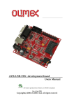
1
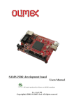
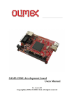
CS-E9302 development board
Users Manual
Rev.A, July 2008
Copyright(c) 2008, OLIMEX Ltd, All rights reserved
INTRODUCTION:
CS-E9302 is powerful development board for 200MHz Cirrus Logic EP9302
ARM920T microprocessors with two USB hosts, two RS232 ports, 100Mbit
Ethernet, SD-MMC card, 16MB NOR Flash, 32MB SDRAM, IrDA
transciever, JTAG, UEXT, EXT, ADC connectors for additional peripherials.
BOARD FEATURES:
-
-
-
MCU: EP9302 ARM920T 200Mhz, 16+16KB instruction and data
cache, MMU, SDRAM, SRAM, FLASH external bus controller 100Mhz
bus, 100Mbit Ethernet MAC, two UARTS, two USB 2.0 ports, IrDA,
ADC, SPI, I2S Audio, AC97, DMA 12 ch, RTC, dual PLL, WDT, 2- 16
bit, 1- 32 bit TIMERS, boot ROM, interrupt controller;
External SDRAM 32MB (16MB x16bit) 7.5 ns /133MHz;
External Flash 16MB (8MB x16 bit) 80 ns;
ETHERNET 10/100 PHY KS8721BL;
2 x RS232 drivers and connectors;
2 x USB host connectors;
SD/MMC card;
IrDA transciever on board;
UEXT connector with I2C, SPI, RS232 and power supply for
connecting add-on modules like RF link, MP3, etc available from
Olimex;
JTAG interface;
ADC extension port;
Power supply plug in jack;
Linux 2.4, Linux 2.6 and NetBSD sources and pre-build images
ready to load with Redboot are available on the supplement CD;
Dimensions: 110x90 mm (4.3 x 3.5").
ELECTROSTATIC WARNING:
The CS-E9302 development board is shipped in protective anti-static
packaging. The board must not be subject to high electrostatic potentials.
General practice for working with static sensitive devices should be applied
when working with this board.
BOARD USE REQUIREMENTS:
Cables:
Two DB9 female-female null modem type for connection with
serial COM port of PC host.
Crossed LAN cable for connection with PC or straight LAN
cable for connection with switch or router.
Hardware:
+5V/1A regulated power source.
ARM-JTAG, ARM-USB-OCD, ARM-USB-TINY or other
compatible tool only if you want to develop with JTAG,
usually with the pre-loaded linux RTOS this is not
necessary.
Software:
The boards are delivered pre-loaded with Linux 2.6.
PROCESSOR FEATURES:
The EP9302 system-on-chip processor has the following features:
● 200 MHz ARM920T Processor
▬ 16 KByte data cache and 16 KByte instruction cache
▬ MMU enabling Linux® and Windows® CE
▬ 100 MHz system bus
● MaverickKey™ IDs for Digital Rights Management or Design IP
Security
▬ 32-bit unique ID
▬ 128-bit random ID
● Integrated Peripheral Interfaces
▬ 1/10/100 Mbps Ethernet MAC
▬ Two-port USB 2.0 Full Speed host (OHCI)
▬ Two UARTs (16550 Type)
▬ IrDA interface, slow and fast mode
▬ Analog-to-Digital Converter (ADC)
▬ Serial Peripheral Interface (SPI) port
▬ AC ‘97 interface
▬ I2S interface, up to 2 channels
● External Memory Options
▬ 16-bit SDRAM interface, up to four banks
▬ 16/8-bit SRAM/Flash/ROM interface (I/F)
▬ Serial EEPROM interface
● Internal Peripherals
▬ Real-Time clock with software trim
▬ 12 DMA channels for data transfer that maximizes system
performance
▬ Boot ROM
▬ Dual PLLs control all clock domains
▬ Watchdog timer
▬ Two general purpose 16-bit timers
▬ General purpose 32-bit timer
▬ 40-bit debug timer
● General-Purpose I/Os
▬ 16 enhanced GPIOs including interrupt capability
▬ 31 additional optional GPIOs multiplexed on peripherals.
EP9302 BLOCK DIAGRAM
MEMORY MAP:
Address Range
Sync Memory Boot
Async Memory Boot
ASD0 Pin = 1
ASD0 Pin = 0
Async memory (nCS0)
Sync memory (nSDCE3)
0xE000_0000 - 0xEFFF_FFFF
Sync memory (nSDCE2)
Sync memory (nSDCE2)
0xD000_0000 - 0xDFFF_FFFF
Sync memory (nSDCE1)
Sync memory (nSDCE1)
0xC000_0000 - 0xCFFF_FFFF
Sync memory (nSDCE0)
Sync memory (nSDCE0)
0x9000_0000 - 0xBFFF_FFFF
Not Used
Not Used
0x8080_0000 - 0x8FFF_FFFF
APB mapped registers
APB mapped registers
0x8010_0000 - 0x807F_FFFF
Reserved
Reserved
0x8000_0000 - 0x800F_FFFF
AHB mapped registers
AHB mapped registers
0x7000_0000 - 0x7FFF_FFFF
Async memory (nCS7)
Async memory (nCS7)
0x6000_0000 – 0x6100_0000 (16MB on
board NOR flash)
Async memory (nCS6)
Async memory (nCS6)
0x5000_0000 - 0x5FFF_FFFF
Reserved
Reserved
0x4000_0000 - 0x4FFF_FFFF
Reserved
Reserved
0x3000_0000 - 0x3FFF_FFFF
Async memory (nCS3)
Async memory (nCS3)
0x2000_0000 - 0x2FFF_FFFF
Async memory (nCS2)
Async memory (nCS2)
0x1000_0000 - 0x1FFF_FFFF
Async memory (nCS1)
Async memory (nCS1)
0x0001_0000 - 0x0FFF_FFFF
Sync memory (nSDCE3)
Async memory (nCS0)
0xF000_0000 – 0xF200_0000 (32MB
on board SDRAM)
SCHEMATIC:
BOARD LAYOUT:
POWER SUPPLY CIRCUIT:
CS-E9302 power supply should be 5V regulated, please do not use other
than 5V power supply as the power line goes to the USB hosts and if you
apply power supply above 5V this will destroy your USB devices. The
PWR_JACK inner pin is positive.
The board power consumption is about 400-450 mA with 200 MHz CPU
clock and 100MHz system bus.
RESET CIRCUIT:
The EP9302 chip can be reset through the PRSTN pin(power on reset) or
through the open drain common reset pin(user reset) - RSTON pin.
PRSTN is a Power-on Reset realized with MCP130T Reset circuit with typical
2.9V threshold. On the board is present a PRN button which is used for
manual Power-on Reset.
The user reset – RSTON is common for the CS9203 microcontroller, PHY
chip, NOR flash, JTAG and MCP130 Supervisory circuit.
It can be
generated from JTAG pin(15), RSTN button, CS9302 or MCP130T Reset
circuit.
CLOCK CIRCUIT:
EP9302 generates its internal clock with PLL and uses single14.7456 MHz
crystal connected to EP9302 pin 119 (XTAL0) and pin 118 (XTAL1).
The Real Time Clock operates from a 32.768 KHz crystal.
JUMPER DESCRIPTION:
Boot configuration jumpers:
The Hardware Configuration controls are defined by a set of device pins that
are latched into configuration control bits on the assertion of chip reset on
the rising edge of the PRSTN or RSTON pin. The different hardware
configuration bits define watchdog behavior, boot mode (internal or
external), boot synchronicity, and external boot width. The latched pins are:
EECLK
– Select internal or external boot
The corresponding jumper is EECLK_L. When the
jumper is closed EECLK pin is log. “0”, otherwise – log.”1”.
EEDAT
– Should be pulled up to “1”
The corresponding jumper is EEDAT_L. When the
jumper is closed EEDAT pin is log. “0”, otherwise – log.”1”.
TEST[1:0]
– Select boot mode
The corresponding jumpers are T0_H/T0_L and T1_H/T1_L
When the T0_H/T0_L jumper is closed to T0_H side TEST0
pin is “1”. When the T0_H/T0_L jumper is closed to T0_L
side TEST0 pin is “0”.
When the T1_H/T1_L jumper is closed to T1_H side TEST1
pin is “1”. When the T1_H/T1_L jumper is closed to T1_L
side TEST1 pin is “0”.
ASDO
– Select synchronous or asynchronous boot
The corresponding 3 pin jumper is ASDO_H/ASDO_L. If the
jumper is closed to ASDO_H side – ASDO pin is log. “1”.
The Other side is log. “0”.
CSN[7:6]
– Select external boot width.
CSN6 and CSN7 are the jumpers which define logical level
of these pins. If the jumpers are closed – the corresponding
pin is “0”.
EECLK EEDAT TEST1 TEST0 ASDO CSN[7:6] Boot Configuration
0
1
0
0
1
00
01
External boot from Sync memory space selected by
DevCfg3 through the SDRAM Controller. The
media type must be either SROM or SyncFLASH.
The selection of the SRAM width is determined by
latched CSN[7:6] value:
8-bit SFLASH
16-bit SROM
0
1
0
0
0
00
01
External boot from Async memory space selected by
nCS0 through Synchronous Memory Controller. The
selection of the SRAM width is determined by
latched CSN[7:6] value:
8-bit SRAM
16-bit SRAM
1
1
0
1
X
01
16-bit SERIAL BOOT
00
01
Boot from external NOR-FLASH. The selection of
the bus width is determined by latched CSN[7:6]
value:
8-bit
16-bit – DEFAULT POSITION – NORMAL BOOT
00
01
Internal boot from on-chip ROM. The selection of
the ROM width is determined by latched CSN[7:6]
value:
8-bit
16-bit
1
1
1
1
0
0
0
0
1
0
Only two selections are functional for the user, Normal Boot and Serial
Boot. The other modes are reserved for factory use only.
The BLUE table line is the default boot position.
Watchdog configuration jumpers:
CSN1
- Disable Watchdog reset timer
CSN2
If the CSN1 jumper is closed the corresponding pin
(CSN1) is “0”, otherwise – “1”.
- Disable Watchdog reset duration
If the CSN2 jumper is closed the corresponding pin
(CSN2) is “0”, otherwise – “1”.
CSN1
CSN2
Startup Option
0
0
Watchdog Disabled; Reset Duration
Disabled
0
1
Watchdog Disabled; Reset
Duration Active
1
0
Watchdog Active; Reset
Duration Disabled
1
1
Watchdog Active; Reset
Duration Active
The BLUE table line is the default boot position.
WPD/WPE
The WPD/WPE jumper defines Write protected state
of NORFLASH U2(JS28F128J3C120)
WPD state (1-2 shorted) enables flash write, WPE
state (2-3
shorted) disables flash write.
Default position is 1-2 shorted.
EE_WP
When the EE_WP jumper is , it closed disables
U7(AT25F1024)
EEPROM write.
Default position is open.
IRDA/RXD1
The IRDA/RXD1 jumper defines RXD1(pin 110 of
MCU) connection. When the jumper is installed in IRDA
state (2-3
shorted), then the RXD1 function of MCU is
connected to IRDA module. If RXD1 state is selected (1-2
shorted), RXD1 pin is
connected through
RS232
driver U5 to RS232_1 connector.
Default position is 1-2 shorted.
IRDA/TXD1
The IRDA/TXD1 jumper defines TXD1(pin 114 of
MCU) connection. When the jumper is installed in IRDA
state (2-3
shorted), then TXD1 function of MCU is
connected to IRDA module. If TXD1 state is selected (1-2
shorted), TXD1 pin is
connected through
RS232
driver U5 to RS232_1 connector.
Default position is 1-2 shorted.
IRDA_LS_E
IRDA_LS_E jumper is used if Low Speed mode of
IRDA chip
must be selected. When the jumper is closed,
the user enables
Low Speed mode.
Default position is open.
RST_E
When the RST_E jumper is closed, pin15 of JTAG
connector is
tied to RSTN (User Reset) line or allows JTAG
reseting.
Default position is closed.
UEXT/RXD0
The UEXT/RXD0 jumper defines RXD0(pin 109 of
MCU) connection. When the jumper is installed in UEXT
state, then the
RXD0 function of MCU is connected to
the UEXT connector. If
RXD0 state is selected, RXD0
pin is connected through RS232
driver U5 to RS232_0
connector.
Default position is 1-2 shorted.
INPUT/OUTPUT:
Two reset buttons with names RSTN and PRN – connected to EP9302 chip
pin 124 (RSTON) and pin 125 (PRSTN).
One user button with name BUT – connected to EP9301 pin 201 HGPIO[4].
Two LEDs – RED – connected to EP9301 pin 98 RDLED and GREEN –
connected to EP9301 pin 97 GRLED.
Power supply red LED with name PWR – indicates that power supply is
present.
CONNECTOR DESCRIPTIONS:
USB1, USB2:
USB2
USB1
Pin # Signal Name
Pin # Signal Name
1
+5V
1
+5V
2
USBM0
2
USBM2
3
USBP0
3
USBP2
4
GND
4
GND
USBM0 and USBP0 form the differential input/output of the USB host 0.
USBM1 and USBP1 form the differential input/output of the USB host 1.
The USB Open Host Controller Interface (Open HCI) provides full speed serial
communications ports at baud rate of 12 Mbits/sec. Up to 127 USB devices (printer, mouse,
camera, keyboard, etc.) and USB hubs can be connected to the USB host in the USB
“tieredstart” topology. The USB port is compliance with the USB 2.0 specification and
supports both low speed (1.5 Mbps) and full speed (12 Mbps) USB device connections.
RS232_0, RS232_1:
UART0 supports modem bit rates up to 115.2 Kbps, supports HDLC and includes a
16 byte FIFO for receive and a 16 byte FIFO for transmit. The Shell of the installed linux OS
is available at the RS232_0 DB9 male connector. The terminal settings are 57600kbps, 8
data bits, no parity, 1 stop bit, no flow control.
UART1 contains an IrDA encoder operating at either the slow (up to 115 Kbps),
medium (0.576 or 1.152 Mbps), or fast (4 Mbps) IR data rates. It also has a 16 byte FIFO for
receive and a 16 byte FIFO for transmit.
RS232_0
RS232_1
Pin # Signal Name
Pin # Signal Name
1
NC
1
NC
2
RXD_0
2
RXD_1
3
TXD_0
3
TXD_1
4
pin 6
4
pin 6
5
GND
5
GND
6
pin 4
6
pin 4
7
pin 8
7
pin 8
8
pin 7
8
pin 7
9
NC
9
NC
TXD_0 OutputTransmit Data 0. This is the asynchronous serial data output (RS232) for
the shift register on
the UART0 controller. (This pin is input for the RS232 and
input for the LPC2478)
RXD_0Input Receive Data 0. This is the asynchronous serial data input (RS232) for the
shift register on the UART0 controller. (This pin is output for the RS232 and
input for the LPC2478)
TXD_1 OutputTransmit Data 1. This is the asynchronous serial data output (RS232) for
the shift register on
the UART1 controller. (This pin is input for the RS232 and
input for the LPC2478)
RXD_1Input Receive Data 1. This is the asynchronous serial data input (RS232) for the
shift register on the UART1 controller. (This pin is output for the RS232 and
input for the LPC2478)
ETHERNET:
The CS-E9302 is shipped with a complete physical and MAC subsystem. The EP9302
supports 1/10/100 Mbps transfer rates. The MAC subsystem is compliant with the
ISO/TEC 802.3 topology for a single shared medium with several stations. Multiple MIIcompliant PHYs are supported. The PHY layer is realized with MICREL PHY chip KS8721BL.
Pin #
Signal Name Chip Side
Pin #
Signal Name Chip Side
1
TD+
5
NC
2
TD-
6
2.5V
3
2.5V
7
RD+
4
NC
8
RD-
LED
Right
Color
Yellow
Usage
Activity
Left
TDTD+
RDRD+
Green
OutputDifferential
OutputDifferential
Input Differential
Input Differential
signal
signal
signal
signal
100MBits/s (Half/Full duplex)
output. This signal is output from the MCU.
output. This signal is output from the MCU.
input. This signal is input for the MCU.
input. This signal is input for the MCU.
UEXT:
Pin # Signal Name
Pin # Signal Name
1
3.3V
2
GND
3
TXD0
4
RXD0_UEXT
5
H2
6
H3
7
SSPRX1
8
SSPTX1
9
SCLK1
10
SFRM1
UEXT is a universal OLIMEX connector with 3.3V power supply and UART, SPI
interface + MCU HGPIO[2] and HGPIO[3] port connected to UEXT pin 5 and pin 6. Other
device or modules with these interfaces can connected with UEXT. For example:
MOD-NRF24L - http://www.olimex.com/dev/mod-nrf24L.html
MOD-RFID125- http://www.olimex.com/dev/mod-rfid125.html
MOD-MP3 - http://www.olimex.com/dev/mod-mp3.html
ADC:
Pin # Signal Name
Pin # Signal Name
1
GND
2
GND
3
ADC0
4
ADC1
5
ADC2
6
ADC3
7
ADC4
8
9
GND
10
ADC_VDD(3.3V)
GND
The ADC block consists of a 12-bit Analog To Digital converter with a analog input
multiplexer. The multiplexer can select to measure battery voltage and other miscellaneous
voltages on the external measurement pins. Signal should be in range: 0 to 3.3 V, ADC
complete may issue interrupts.
SD/MMC CARD INTERFACES
Pin #
Signal Name
1
CD_MMC_E/SFRM1
SSPTX1
GND
VCC (470nH to 3.3V)
SCLK1
GND
SSPRX1
10K to VCC
10K to VCC
WP (33K to VCC)
WP (2K to GND)
CP (2K to GND)
WP (33K to VCC)
2K to GND
2K to GND
2
3
4
5
6
7
8
9
10
11
12
13
14
15
EXT:
Pin #
Signal Name
Pin #
Signal Name
1
CGPIO[0]
2
EGPIO[15]
3
EGPIO[14]
4
EGPIO[13]
5
EGPIO[12]
6
EGPIO[11]
7
EGPIO[10]
8
EGPIO[9]
9
EGPIO[8]
10
EGPIO[7]
11
EGPIO[6]
12
EGPIO[5]
13
EGPIO[4]
14
EGPIO[3]
15
EGPIO[2]
16
EGPIO[1]
17
EGPIO[0]
18
FGPIO[1]
19
FGPIO[2]
20
FGPIO[3]
21
HGPIO[2]
22
HGPIO[3]
23
HGPIO[4]
24
HGPIO[5]
25
ABITCLK
26
ASYNC
27
ASDI
28
ASDO
29
ARSTN
30
+5V(Out)
31
3.3V(Out)
32
1.8V(Out)
33
GND
34
PRN(Power on Reset)
On this connector are available all GPIOs of EP9302 which are not used for other
purposes. With them you can make add-on modules to control with CS-E9302 like
GSM/GPS, input/output add-on boards.
JTAG:
The JTAG connector allows the software debugger to talk via a JTAG (Joint Test
Action Group) port directly to the core. Instructions may be inserted and executed by the
core thus allowing MCU memory to be programmed with code and executed step by step by
the host software.
For more details refer to IEEE Standard 1149.1 - 1990 Standard Test Access Port.
Pin # Signal Name
Pin # Signal Name
1
+3.3V
2
+3.3V
3
TRST
4
GND
5
TDI
6
GND
7
TMS
8
GND
9
TCK
10
GND
11
TCK/GND
12
GND
13
TDO
14
GND
15
RSTN/NC
16
GND
17
NC
18
GND
19
NC
20
GND
TDI
Input Test Data In. This is the serial data input for the shift register.
TDO OutputTest Data Out. This is the serial data output for the shift register. Data is
shifted out of the
device on the negative edge of the TCK signal.
TMS Input Test Mode Select. The TMS pin selects the next state in the TAP state
machine.
TCK Input Test Clock. This allows shifting of the data in, on the TMS and TDI pins. It is
a positive edge
triggered clock with the TMS and TCK signals that define the
internal state of the device.
TRST Input Test Reset. This signal resets the JTAG controller.
TCK OutputClock. This is a synchronization signal which the JTAG connector uses to
acknowledge it is
ready to receive/transmit.
RSTN Input Reset. This signal resets the MCU.
This connector shares the ARM default JTAG layout.
PWR:
Pin # Signal Name
1
+5VDC ONLY
2
GND
Note: Apply only 5V DC regulated voltage!
MECHANICAL DIMENSIONS:
All measures are in mm.
SOFTWARE:
CS-E9302 is distributed with CD with Linux 2.4, NetBSD and Linux 2.6
sources and pre-build images for Linux 2.4, Linux 2.6 and NetBSD.
The boards are pre-loaded with Linux 2.6 in the internal flash.
The software for CS-E9302 could be developed and debugged on desktop
computer then cross-compiled and loaded in the board. Here below is example how to cross
compile “Hello world” program. In most of the cases you do not need JTAG as on the other
embedded systems which do not have RTOS (how often do you develop on your Pentium
desktop computer with JTAG?), but for case where peoples want to blink LEDs without
RTOS we have provided the JTAG connector as well.
Cross-compiling a simple "hello world" example:
Extract one of the provided cross-compilers on your host system and add it to the
PATH variable. Use the cross-compiler to build the example, then transfer it to the
board by e.g. USB flash drive, http download etc.
Example commands:
----- On the host system ----# cd /usr/local/arm
# tar xjf arm-linux-gcc-4.1.1-920t.tar.bz2
...
$ PATH=$PATH:/usr/local/arm/4.1.1-920t/bin
$ cat > hello.c
#include <stdio.h>
int main(void)
{
unsigned int i;
printf("\r\nProba proba ");
for (i=0; i<10; i++)
printf("\r\n%d", i);
return 0;
}
^D
$ arm-linux-gcc -o hello hello.c
$ cp hello ~/htdocs/
----- On the board ----~ # wget http://192.168.0.xx/hello
~ # chmod 777 hello
~ # ./hello
Proba proba
0
1
ORDER CODE:
CS-E9302 – assembled and tested (no kit, no soldering required)
How to order?
You can order to us directly or by any of our distributors.
Check our web www.olimex.com/dev for more info.
All boards produced by Olimex are RoHS compliant
Revision history:
REV.A
- created July 2008
Disclaimer:
© 2008 Olimex Ltd. All rights reserved. Olimex®, logo and combinations thereof, are
registered trademarks of Olimex Ltd. Other terms and product names may be trademarks of
others.
The information in this document is provided in connection with Olimex products. No
license, express or implied or otherwise, to any intellectual property right is granted by this
document or in connection with the sale of Olimex products.
Neither the whole nor any part of the information contained in or the product described in
this document may be adapted or reproduced in any material from except with the prior
written permission of the copyright holder.
The product described in this document is subject to continuous development and
improvements. All particulars of the product and its use contained in this document are
given by OLIMEX in good faith. However all warranties implied or expressed including but
not limited to implied warranties of merchantability or fitness for purpose are excluded.
This document is intended only to assist the reader in the use of the product. OLIMEX Ltd.
shall not be liable for any loss or damage arising from the use of any information in this
document or any error or omission in such information or any incorrect use of the product.