1
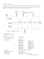
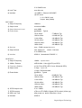
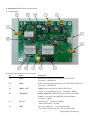
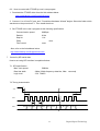
User’s Manual GPS Synchronized Programmable Oscillator GPSG-3G Digital Signal Technology, Inc. 1-7-30 Higashi Benzai, Aska, Saitama 351-0022, Japan TEL: 81-48-468-6094 FAX: 81-48-468-6210 WEB: http://www.dst.co.jp/en email: [email protected] Contents 1 General Description ……………….. 3 2 Specification ……………….. 3 3 Outer dimensions ……………….. 4 4 Appearance and feature for each parts ……………….. 5 5 Control by USB1 ……………….. 6 6 Control by USB2 ……………….. 8 7 Control by SPI serial data ……………….. 9 8 How to switch an internal clock or external clock ……………….. 10 9 Shipping inspection ……………….. 10 10 Warranty ……………….. 10 11 Others ……………….. 10 2 Digital Signal Technology 1. General Description GPSG-3G is an open-framed, non-enclosed signal generator board, equipped with PCK3GF-1, REF10MF and GPS synchronized 10MHz reference clock. GPSG-3G can generate your desired clock signal with 1KHz resolution in an extremely wide band of 50MHz ~3000MHz. 2. 2.Specifications 2-1. Electrical Specifications PCK3GF-1 1) Output Frequency Range 50~3000MHz 2) Frequency Resolution 1KHz 3) Phase Noise @3GHz Typical 10 Hz offset : -46 dBc/Hz Typ. 100 Hz offset : -86 dBc/Hz Typ. 1 KHz offset : -104 dBc/Hz Typ. 10 KHz offset : -109 dBc/Hz Typ. 100 KHz offset : -106 dBc/Hz Typ. 1MHz offset : -135 dBc/Hz Typ. 10MHz offset : -156 dBc/Hz Typ. 4) Spurious Max. -65dBc (Except harmonics) 5) Output Harmonic Level Max. 6) Output Level More than +10dBm 7) Lock Output lock: High level 3 -8dBc unlock: Low level Digital Signal Technology 3.3V CMOS level 8) Lock Time max 40m sec 9) Interface (1) USB2.0 (Shared REF10MF) (2) SPI serial 3.3V CMOS level 3 bytes date (24bits) REF10MF 1) Output Frequency 100MHz 2) Output Level more than 0dBm 3) Output Harmonic Level max -8dBc 4) Phase Noise @100MHz Typical 10 Hz offset : -77 dBc/Hz Typ. 100 Hz offset : -119 dBc/Hz Typ. 1 kHz offset : -142 dBc/Hz Typ. 10 kHz offset : -154 dBc/Hz Typ. 100 kHz offset : -160 dBc/Hz Typ. 1MHz offset : -162 dBc/Hz Typ. 4) Spurious max -70dBc (except harmonic 5) Output Unlock lock: High level unlock.: Low level 3.3V CMOS level 6) Interface USB2.0 (shared with PCK3GF-1) GPSTCXO 1) Output Frequency 10MHz square wave 2) 10MHz Retrace ±2E-08 After 1 Hour @+25℃(no GPS) 3) Frequency Stability ±1.5e-07(no GPS),<5E-12 over 24hrs(with GPS) 4) Output Level 3.3Vpp open end 1.5Vpp 50Ω terminated 5) Phase Noise @10MHz Typical 10 Hz offset : -99 dBc/Hz Typ. 100 Hz offset : -126 dBc/Hz Typ. 1 kHz offset : -140 dBc/Hz Typ. 10 kHz offset : -142 dBc/Hz Typ. 100 kHz offset : -149 dBc/Hz Typ. 1MHz offset : -150 dBc/Hz Typ. 6) 1PPS Output Level 3.3V CMOS 7) 1PPS Accuracy ±75ns to UTC RMS(1-Sigma) GPS Locked (<20ns typ) 8) GPS Lock Time after power-on about 30minutes~1hour 9) Interface USB2.0 4 Digital Signal Technology Common Specifications 1) Supply Voltage +5V +/- 5% max 750mA 2) Dimensions 110x90(mm) 3) Operating Temperature Range 0 ~ +60 degreeC 4) Storage Temperature Range -30 ~ +70 degreeC 5) Accessory GPS antenna(with BNC connector)10M 1 MMCX/BNC adapter cable 15cm 1 USB cable 1.5M 2 2-3. Phase noise (typ value) 3. Outer Dimensions 5 Digital Signal Technology 4. Appearance and Feature for each parts 4-1. Appearance 4-2. Name and description for each part No. Name Description J1 USB1 USB communications interface pin for GPSTCXO. Connector : USB-Mini-B. J2 USB2 USB communications interface pin for REF10MF, PCK3GF-1. Connector : USB-Mini-B. J4 10MHz OUT 10MHz Output terminal of 10MHz GPSTCXO. Levels : 3.3V CMOS(open end) J5 MONI/EXT Connector : SMA-J. Monitor output for 100MHz reference clock of REF10MF. Output Level: more than 0dBm(50 ohm terminated) Connector : SMA-J J6 RF OUT Signal output Connector: SMA-J Output impedance : 50 ohm J7 PWR 5V power supply pin 2 pin screw terminal Connector Part Number: ML-35A-2P (Sato Parts) 6 Digital Signal Technology No. Name Description J10 EXT/INT Internal and external switching pin of REF10MF. J11 HEADER interface SPI Control , unlock signal, power supply pin. 2.54mm pitch 5x2 pin header connector Connector Part Number: PS-10PE-D4T1-PN1 (JAE) J14 1PPS OUT 1PPS output terminal of GPSTCXO. Connector :SMB-J GPS_J3 GPS ANT IN level : 3.3V CMOS GPS antenna input pin of GPSTCXO Connector:MMCX. Connect GPS antenna with 15cm MMCX-BNCJ conversion cable D1 GPSLOCK1 LED lights when synchronized to GPS. D2 REFLOCK LED lights when synchronized to an external 10MHz clock. LED doesn’t light in case of the internal clock because VCO is free-run. D3 GPS_D3 PCKLOCK LED lights when sychronized to an external 100MHz clock. GPSLOCK2 Red LED and Green LED Both of them lights for a second and soon goes off when the power is turned on. As soon as the Red LED begins to blink, the internal TCXO starts to lock to UTC. After 30 minutes to 1 hour, Green LED lights. 4-3. J11 Connector and pin assignment No. Name Description 1 GND Power Supply/signal GND 2 GND Power Supply/signal GND 3 +5V Power input +5V Not using the PWR connector. the power can be supplied from here. 4 +5V the same as above 5 LOCK PLL lock status output of PCK3GF-1 3.3V CMOS. 6 /CS Chip select under SPI mode Input low active 3.3V CMOS Internally pulled up. 7 LOCK PLL lock status output of REF10MF. 3.3V CMOS. 8 SDI Serial data input under SPI mode 7 Digital Signal Technology 3.3V CMOS. 9 LOCK GPS signal output of GPSTCXO. 3.3V CMOS 10 CLK Serial clock input under SPI mode. 3.3V CMOS. 5. Control by USB 1 communication(GPSTCXO) 5-1. Refer to the following User's Manual for detailed specifications such as commands, GPSTCXO http://www.dst.co.jp/pdf_file/gpstcxo.pdf 5-2. Device The device is FT232R manufactureed by FTDI (See item 6 for more information about the driver software.) 5-3. Set the communication setting of PC as below Speed 115200bps Data bits 8 bits Stop bit 1 bit Parity none Flow control none 6. Control by USB2 communication(REF10MF, PCK3GF-1) The interface of start/stop synchronization is used by USB communication. The device is FT232R manufactured by FTDI. There are two ways to control; one is to control from the virtual COM port of PC and another is to control FT232R directly by user’s own program. 6-1. Procedure 1) Download the FT232R drivers from the link addressed below and then unzip it to a folder. http://www.ftdichip.com/Drivers/VCP.htm Procedure 2) Use USB cable to connect J1 or J2 and PC. “ Found New Hardware Wizard” will begin, and then select the folder where you downloaded. Finally install the driver. Procedure 3) Set the communication setting of PC as below. Speed 9600bps Data bits 8 bits Stop bits 1 bit Parity none Flow control none 8 Digital Signal Technology Any communication software such as Hyperterminal can be used for setting from the virtual COM of PC. 6-1-1. Command definition(PCK3F-1, REF10MF) Character strings enclosed in double quotation marks “ “ means ASCII code, and CR and LF, which are control codes, means 0D(hex) and 0A(hex). If any invalid command is entered, “INVALID DATA “CR LF “*” is returned. All characters used for input should be uppercase. If a normal command is entered, “ * “ is returned. Also, the entered data is echoed back. GPSG-3G is consisted of GPSTCXO, PCK3GF-1 and REF10MF but PCK3GF-1 and REF10MF is controlled by SCI serial communication. In case of controlling REF10MF, put always “ $ “ in front of the command. 6-1-2. Frequency setting command (PCK3GF-1) For frequency setting, input can be made in MHz, KHz and Hz unit. (1) Setting in MHz For setting 2450MHz, input the following data. “2400M”CR In this case, all the data below 100KHz is set to “0”. (2) Setting in KHz For setting 2400002KHz, input the following data. “2400002K”CR Also the following expression is allowed. “2400002”CR 6-1-3. READ command (PCK3GF-1) By entering “READ”CR, the currently set frequency is output. The response is as shown below. “ffffffffKHz”CR LF “fffffff” is the frequency of currently set in KHz unit. 6-1-4. SAVE command (PCK3GF-1) By entering “SAVE”CR, the current frequency can be memorized into EEPROM. When the power is on next time, the stored data can be output. 9 Digital Signal Technology 6-1-5. REF command (PCK3GF-1) REF frequency can be changed to 50MHz or 100MHz by entering “REF”CR. The inputted frequency can be memorized into the EEPROM and the last saved frequency can be recalled even if power is off. The following response is returned. CURRENT_xxMHz Enter ‘1’ for 50MHz ‘2’ for 100MHz >> The current REF frequency is displayed on xx. Enter 1 or 2 and the following response is returned. ARE YOU SURE? Enter “Y”>> By entering “ Y “ the selected REF frequency stored in the EEPROM will be enabled. 6-1-6. Caution for setting data consecutively (PCK3GF-1) In case of switching frequency at high speed, data may drop out because the PCK3GF-1 does not use flow control. Upon completion of processing by sending a frequency setting command in 6-3-1, the prompt “*” is returned; therefore, confirm the receiving of this prompt, and then send the next frequency setting command. 6-1-7. Internal clock frequency adjustment command(REF10MF) Adjust the frequency by entering ”$ADJ_xxx” CR. OFFSET is given in xxx with 2’ complement HEX data. Enter 000 for OFFSET 0 Enter 100 for stepping the frequency up Enter F00 for stepping the frequency down max 800 max 7FF The numeric value itself cannot be converted to frequency, but LSB is appropriated to approximately 2.65Hz. Once frequency is successfully set, it is automatically memorized in EEPROM. And the last saved frequency can be recalled when power is on next time. 6-1-8. STAT command (REF10MF) By entering “$STAT”CR, the currently set parameters are output, such as internal offset value, PLL lock status and EXT/INT condition. ADJ=xxx xxx is SDJ OFFSET value and shows in 2’ complement LOCK=y y is the LOCK CONDITION 1: LOCK 0: UNLOCK EXT/INT=z z is a CLOCK MODE 1: External clock mode 2: Internal clock mode 10 Digital Signal Technology 6-2. How to control with FT232R by user’s own program 1. Download the FT232R driver from the link address below. http://www.ftdichip.com/Drivers/D2XX.htm 2. Connect J1 or J2 into PC port, and “ Found New Hardware Wizard” begins. Select the folder which was done on the procedure 5-1. Then install the driver. 3. Set FT232R in the user’s program as the following specification. Communication speed 9600bps Data bit 8 bits Stop bit 1 bit Parity none Flow control none Also, refer to the link address below. http://www.ftdichip.com/Support/Links.htm 7 Control by SPI serial data How to set using SPI interface is explained below. 7-1. SPI specification Max. clock speed 500KHz Data bits width 24bits (22bits frequency data bits, 2bits reserved) Logic level 3.3V CMOS 7-2 Timing characteristic t1 /CS t2 t5 CLK t4 t3 SDI D23 D22 D21 D20 D19 D18 11 D19 D2 D1 D0 Digital Signal Technology Timing characteristic Parameter 7-3. Condition Min. Unit t1 CLK setup time to /CS 50 ns t2 CLK period 2 us t3 SDI setup time to CLK rise edge 100 ns t4 SDI hold time to CLK rise edge 100 ns t5 /CS set up time to CLK rise edge 50 ns Command definitions 24 bits frequency data is transferred by serial data. Actual frequency data bits are 22 bits among 24 bits, the remaining 2 bits are not used. Bit definition is as follows Bits Name Width Description bit[23:22] Reserved 2 bits Not used, Do not care bit[21:0] Frequency 22 bits Frequency data in 1 KHz resolution in binary For example, if you set 2456000KHz, frequency data of KHz unit must be converted to binary data. 2456000KHz is converted to 2579C0 hex in 22 bits binary data. 8. How to switch an external clock or Internal Clock Switching an external clock or internal clock is available at J10. Jumper for an external clock mode Jumper for an internal clock mode 9. Shipping inspection 100% inspection shall be performed for the electrical specification in 2-1. 10. Warranty If any defect is found due to the manufacturer’s improper production or design within one year after delivery, repair or replacement shall be performed a the manufacturer’s responsibility. DS Technology, Inc. assumes no liability for damages that may occur as a result of handling by users even though the warranty period. 12 Digital Signal Technology 11. Others 11-1. This product, which employs a CMOS device may be easily damaged by static electricity. DS Technology, Inc. assumes no liability for damages that may occur as the result of handling by users even though the above warranty period. 11-2. Do not supply over voltage power supply, module may be damaged. DS Technology, Inc assumes no liability for damages that may occur as the result of handling by users even though the above warranty period. Descriptions of this manual are subject to change without notice. No portion of this manual can be reproduced without the permission of Digital Signal Technology. Digital Signal Technology assumed no liability for damages that may occur as a result of handling by users. The contents of this manual do not apply to the warranty in executing an industrial property or other rights, nor permission for the right of execution. Digital Signal Technology assumes no responsibility for the third party’s industrial property occurred from using the circuits described in this manual. 13 Digital Signal Technology