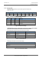
1
TAGnology RFID GmbH | Grazer Vorstadt 142 | 8570 Voitsberg | AUSTRIA phone: +43 (0)3142/ 28 9 28-10 | fax: +43 (0)3142/ 28 9 28-20 | [email protected] | www.tagnology.com LF MultiTag R/W Module USER MANUAL © 2008 HID Global Corporation. All rights reserved. 0000-USM-01-0-01 Firmware Version 1.0 November 4, 2008 Doc Number: 0000-USM-01, Rev A.0 0000-USM-01-0-01 LF MultiTag R/W Module User Manual, Firmware V1.0 Warning - Read before start-up! • The product may only be used for the intended purpose designed by for the manufacturer. The operation manual should be conveniently kept available at all times for each user. • Unauthorized changes that have not been sold or recommended by the manufacturer may have a negative influence on the system the program has been installed or copied on. Such unauthorized measures shall exclude any liability by the manufacturer. • The liability-prescriptions of the manufacturer in the issue valid at the time of purchase are valid for the device. The manufacturer shall not be held legally responsible for inaccuracies, errors, or omissions in the manual or automatically set parameters for a device or for an incorrect application of a device. • Only qualified personnel should carry out installation, operation, and maintenance procedures. • Use of the program and its installation must be in accordance with national legal requirements. • When working on devices the valid safety regulations must be observed. • International copyrights are applicable to this program. Unauthorized copying, distribution or resale of this program or of parts of this program is a violation of applicable laws and will be prosecuted. Page 2 of 58 November 4, 2008 © 2008 HID Global Corporation. All rights reserved. LF MultiTag R/W Module 0000-USM-01-0-01 User Manual, Firmware V1.0 Read Me First About This Guide This manual describes the LF MultiTag R/W Module. Its goal is to describe the reader, how it works, how to integrate it and how to use it. Contacts Europe, Middle East and Africa HID Global Corporation, Ltd. (Haverhill, UK) email: [email protected] main: +44 (0) 1440 714 850 support: +44 (0) 1440 711 822 fax: +44 (0) 1440 714 840 November 4, 2008 Page 3 of 58 © 2008 HID Global Corporation. All rights reserved. 0000-USM-01-0-01 LF MultiTag R/W Module User Manual, Firmware V1.0 Contents Warning - Read before start-up! ...................................................................................................2 Read Me First ................................................................................................................................3 About This Guide.................................................................................................................3 Contacts ..............................................................................................................................3 Scope ................................................................................................................................7 Overview ................................................................................................................................7 Definitions............................................................................................................................7 Abbreviations.......................................................................................................................7 1 Tag Organization ...............................................................................................................8 1.1 Supported tags .......................................................................................................8 1.2 EM4x02 ..................................................................................................................8 1.3 EM4x50 ..................................................................................................................8 1.4 Hitag 1 ..................................................................................................................10 1.5 Hitag S..................................................................................................................10 1.6 Hitag 2 ..................................................................................................................12 1.7 EM4x05 (ISO FDXB) ............................................................................................13 1.8 Q5.........................................................................................................................14 1.9 TI-RFID SYSTEMS ..............................................................................................16 2 Hardware ..........................................................................................................................17 2.1 Pin out of OEM Module ........................................................................................17 2.2 Plug-In Reader .....................................................................................................23 3 Software ...........................................................................................................................25 3.1 ASCII Protocol......................................................................................................25 3.2 Binary Protocol .....................................................................................................25 3.3 Instruction Set ......................................................................................................27 Appendix A: Antenna Design......................................................................................................52 Introduction........................................................................................................................52 Test-Antenna.....................................................................................................................52 Appendix B: Getting started........................................................................................................54 Appendix C: References..............................................................................................................55 Appendix D: Approvals / Certificates.........................................................................................56 CE Declaration ..................................................................................................................56 FCC Declaration................................................................................................................57 RoHS Compliance.............................................................................................................58 Page 4 of 58 November 4, 2008 © 2008 HID Global Corporation. All rights reserved. LF MultiTag R/W Module 0000-USM-01-0-01 User Manual, Firmware V1.0 List of Figures Figure 1-1: Protection word ........................................................................................................................... 9 Figure 1-2: Control word................................................................................................................................ 9 Figure 1-3: Hitag 1 memory organization.................................................................................................... 10 Figure 1-4: Hitag S memory organization ................................................................................................... 10 Figure 1-5: Configuration Word................................................................................................................... 10 Figure 1-6: Configuration Byte 0 ................................................................................................................. 11 Figure 1-7: Memory Type ............................................................................................................................ 11 Figure 1-8: Configuration Byte 1 ................................................................................................................. 11 Figure 1-9: LCON register ........................................................................................................................... 11 Figure 1-10: LKP register ............................................................................................................................ 11 Figure 1-11: Configuration Byte 2 ............................................................................................................... 12 Figure 1-12: Configuration Byte 3 ............................................................................................................... 12 Figure 1-13: Hitag 2 memory organization.................................................................................................. 12 Figure 1-14: Configuration block ................................................................................................................. 13 Figure 1-15: EM4x05 (ISO FDXB) .............................................................................................................. 13 Figure 1-16: EM4x05 (ISO FDXB) decoding example ................................................................................ 14 Figure 2-1: Pin out of the reader device...................................................................................................... 18 Figure 2-2: Pin out of jumper 1.................................................................................................................... 18 Figure 2-3: Pin out of jumper 2.................................................................................................................... 19 Figure 2-4: Electrical characteristics of pins................................................................................................ 20 Figure 2-5: Mechanical dimensions of the reader device ........................................................................... 24 Figure 3-1: ASCII protocol frame ................................................................................................................ 25 Figure 3-2: Binary protocol frame................................................................................................................ 25 Figure 3-3: Binary protocol frame 2............................................................................................................. 25 Figure 3-4: Example .................................................................................................................................... 26 Figure 3-5: Command overview .................................................................................................................. 27 Figure 3-6: Error codes ............................................................................................................................... 28 Figure 3-7: EEPROM memory .................................................................................................................... 28 Figure 3-8: Protocol configuration register .................................................................................................. 29 Figure 3-9: Baud rate register ..................................................................................................................... 30 Figure 3-10: Baud rate settings ................................................................................................................... 30 Figure 3-11: Exact baud rates ..................................................................................................................... 30 November 4, 2008 Page 5 of 58 © 2008 HID Global Corporation. All rights reserved. 0000-USM-01-0-01 LF MultiTag R/W Module User Manual, Firmware V1.0 Figure 3-12: Communication settings ......................................................................................................... 30 Figure 3-13: Operation mode register ......................................................................................................... 31 Figure 3-14: Protocol configuration register ................................................................................................ 31 Figure 3-15: Leading character of continuous read mode .......................................................................... 35 Figure 3-16: LED response ......................................................................................................................... 37 Figure 3-17: Time slot formula .................................................................................................................... 39 Figure 3-18: Timing diagram of time slotted answers ................................................................................. 40 Figure 3-19: List of leading characters........................................................................................................ 42 Figure 3-20: Read USER port return values ............................................................................................... 45 Figure 3-21: Write User port settings .......................................................................................................... 45 Figure 3-22: Block Data............................................................................................................................... 46 Figure 3-23: Block Data............................................................................................................................... 49 Page 6 of 58 November 4, 2008 © 2008 HID Global Corporation. All rights reserved. LF MultiTag R/W Module 0000-USM-01-0-01 User Manual, Firmware V1.0 Scope The LF MultiTag R/W Module is a Read/Write device that supports a wide range of 125 kHz and 134.2 kHz tags. It supports Hitag 1, S and 2, EM 4x02, EM 4x05 (ISO FDXB), EM4x50, Q5 and TI-RFID SYSTEMS. Using an external antenna and a serial interface it can easily be connected to a host or PC. The first part of the manual describes general functions and memory management of several supported tags. A listing of the memory map is given if necessary. The second part gives a detailed description of the pin out and the electrical characteristics of the OEM module. The third part lists the reader command set. Each command is explained in detail and an example illustrates the usage. FAQs highlight general issues using the Low Frequency MultiTag OEM Reader Module. Appendix A introduces the customized antenna design. Overview Definitions Hex notation A hexadecimal value is marked with the suffix ‘h’, i.e. A1h has the value A1 hexadecimal. ASCII notation ASCII characters are listed within apostrophes, i.e. ‘x’ means a decimal based value x. Abbreviations LSB Least significant bit MSB Most significant bit RFU Reserved for future use OTP One time programmable <CR> Carriage return <LF> Line Feed November 4, 2008 Page 7 of 58 © 2008 HID Global Corporation. All rights reserved. 0000-USM-01-0-01 LF MultiTag R/W Module User Manual, Firmware V1.0 1 Tag Organization 1.1 Supported tags Tag Serial Number Read block Write block Properties EM4x02 √ - - 5 bytes R/O EM4x50 √ √ √ 32 x 4 bytes R/W, password HITAG1 √ √ √ 64 x 4 bytes R/W HITAG S √ √ √ 1, 8 or 64 x 4 bytes R/W HITAG2 √ √ √ 7 x 4 bytes R/W, password EM4x05 (ISO – FDXB) √ - - 8 bytes R/O Q5 √ √ √ 8 x 4 R/W, Password TI-RFID SYSTEMS 64 Bit Read/Only √ TI-RFID SYSTEMS 64 Bit R/W √ √ √ 8 bytes R/W TI-RFID SYSTEMS 1088 Bit Multipage √ √ √ 17x8bytes R/W 1.2 8 bytes R/O EM4x02 The EM4x02 label only provides a 5 bytes serial number. The label starts to send its response immediately after entering an energizing field. Each transponder has its own unique serial number, which cannot be changed. For more information refer to [1] 1.3 EM4x50 The EM4x50 has 1 kBit of EEPROM memory, which is organized in 32 blocks of each 4 bytes. The tag supports a password to protect its configuration settings. The UID and the Identification number are laser programmed at the manufacturing process and are Read/Only. All other data is set to 0 as default. For further information refer to [2] 1.3.1 Memory Organization Block Function Access 00h Password write access 01h Protection word Password protected 02h Control word Password protected 03h - 1Fh User memory R/W 20h Device serial number R/O 21h Device identification R/O Page 8 of 58 November 4, 2008 © 2008 HID Global Corporation. All rights reserved. LF MultiTag R/W Module 0000-USM-01-0-01 User Manual, Firmware V1.0 1.3.1.1 Password The password is read protected. A user has to log in before he can change block 00h – 02h. The password is set to 00000000h as default. 1.3.1.2 Protection word Protection word (01h) Bit 31 - 24 Bit 23 - 16 Bit 15 - 8 Bit 7 - 0 End WI Start WI End RP Start RP Figure 1-1: Protection word The protection word is divided into two parts. First part (bit 0, bit 15) specifies the read protection (RP) area. Bit 16 to bit 31 defines the area of the write inhibited (WI) blocks. Write access to the protection word needs a previous log in. 1.3.1.3 Control word Control word (02h) Bit 31 - 17 Bit 16 Bit 15 - 0 RFU PWC on/off RFU Figure 1-2: Control word The password check (PWC) at bit 16 defines the write access to the user area (03h – 1Fh). If it is set a successful log in prior to any write process is mandatory. It does not affect write access to the control word and protection word. 1.3.1.4 User memory The user memory is free to use. Write access depends on password check bit (control word) and write inhibited area of the protection word. If the PWC is set a log in previous to any write command is mandatory. 1.3.1.5 Device serial number, device identification These two blocks are Read/Only and defined at the manufacturing process. They are stored in a specific area of the tag. Block 20h (device serial number) is returned if a tag is selected. November 4, 2008 Page 9 of 58 © 2008 HID Global Corporation. All rights reserved. 0000-USM-01-0-01 LF MultiTag R/W Module User Manual, Firmware V1.0 1.4 Hitag 1 Hitag 1 has 2 kbit EEPROM memory. The memory is organized in 48 blocks. Each block consists of 4 bytes. For further information refer to [3]. 1.4.1 Memory organization Block Function Access 00h Serial number R/O 01h Configuration word R/W 02h – 0F RFU Not accessible 10h – 3Fh User data Read/Write Figure 1-3: Hitag 1 memory organization 1.4.1.1 Serial number The serial number is factory programmed and cannot be changed anymore. It is used to distinguish Hitag 1 tags from each other. 1.4.1.2 Configuration word The configuration word holds information about the tag formatting. Do not alter the contents. Invalid data might inhibit a tag for further operation. 1.4.1.3 User data User data is free for use. 1.5 Hitag S Hitag S has 32, 256 or 2048 bit EEPROM memory. The memory is organized in blocks of 4 bytes. 1.5.1 Memory organization Block Function Access 00h Serial number R/O 01h Configuration word Read/Write 02h – 3Fh User data R/W Figure 1-4: Hitag S memory organization 1.5.1.1 Configuration Word The configuration word consists of 4 Configuration Bytes Configuration word (01h) CON3 (Byte 3) CON2(Byte 2) CON1 (Byte 1) CON 0(Byte 0) Figure 1-5: Configuration Word Page 10 of 58 November 4, 2008 © 2008 HID Global Corporation. All rights reserved. LF MultiTag R/W Module 0000-USM-01-0-01 User Manual, Firmware V1.0 1.5.1.1.1 CON0 The CON 0 byte describes the memory capacity. CON 0 Bit 7 Bit 6 Bit 5 Bit 4 Bit 3 Bit 2 RFU Bit 1 Bit 0 MEMT 1 MEMT 0 Figure 1-6: Configuration Byte 0 1.5.1.1.2 Memory Type MEMT 0 MEMT 1 Memory Type 0 0 32 Bit 0 1 256 Bit 1 0 2048 Bit 1 1 RFU Figure 1-7: Memory Type 1.5.1.1.3 CON1 The CON1 byte specifies the access conditions of the CON1 and CON2 bytes. CON1 is implemented as OTP. CON 1 Bit 7 Bit 6 Bit 5 Bit 4 Bit 3 Bit 2 RFU Bit 1 Bit 0 LCON LKP Figure 1-8: Configuration Byte 1 1.5.1.1.4 LCON LCON Access right CON1 and CON2 0 R/W 1 CON1: R/O CON2: OTP Figure 1-9: LCON register 1.5.1.1.5 LKP LKP Access Right Block 2 and 3 0 R/W 1 R/O Figure 1-10: LKP register November 4, 2008 Page 11 of 58 © 2008 HID Global Corporation. All rights reserved. 0000-USM-01-0-01 LF MultiTag R/W Module User Manual, Firmware V1.0 1.5.1.1.6 CON2 CON2 specifies the access condition of the blocks. If the bit is set all according blocks are Read/Only. This byte is implemented as OTP. CON 2 Bit 7 Bit 6 Bit 5 Bit 4 Bit 3 Bit 2 Bit 1 Bit 0 Block 4–5 Block 6–7 Block 8 – 11 Block 12 – 15 Block 16 – 23 Block 24 – 31 Block 32 – 47 Block 48 – 63 Figure 1-11: Configuration Byte 2 1.5.1.1.7 CON3 The CON3 byte is RFU and should not be changed. CON 3 RFU Figure 1-12: Configuration Byte 3 1.6 Hitag 2 Hitag 2 tags have 256 bits EEPROM which is divided into 8 blocks. Each block consists of 4 bytes. The tag is only supported in password mode [4]. 1.6.1 Memory organization Block Function Access 00h Serial number R/O 01h Password RWD R/W 02h RFU R/O 03h Configuration block R/W 04h – 07h User data R/W Figure 1-13: Hitag 2 memory organization 1.6.1.1 Serial number The serial number is factory programmed and cannot be changed anymore. It is used to distinguish Hitag 2 tags from each other. 1.6.1.2 Password RWD The password RWD and the Password TAG (see Figure 1-14: Configuration block) is used during the mutual authentication process. Changing the password needs a new authentication. Default value is 4D494B52h. Page 12 of 58 November 4, 2008 © 2008 HID Global Corporation. All rights reserved. LF MultiTag R/W Module 0000-USM-01-0-01 User Manual, Firmware V1.0 1.6.1.3 Configuration The Configuration block sets up a tag. The reader only supports password mode. All other modes will not be detected from the reader. Configuration block (03h) Byte 3 Byte 2 Byte 1 RFU Password TAG Byte 0 Figure 1-14: Configuration block The password TAG is used during the authentication. See Password RWD. 1.6.1.4 User data User data is free for use. 1.7 EM4x05 (ISO FDXB) The ISO FDXB tag only provides a 8 byte serial number. The tag starts automatically sending its ID number after entering an energizing field. The data is stored LSB first. 1.7.1 Decoding EM4x05 (ISO FDXB) The data format of the EM4x05 (ISO FDXB) tag is coded as described below. The serial number is divided into three parts: application ID, country code, national ID. EM4x05 (ISO FDXB) Byte 7 Byte 6 Byte 5 Byte 4 National ID Byte 3 Byte 2 Country code Byte 1 Byte 0 Application ID Figure 1-15: EM4x05 (ISO FDXB) 1.7.1.1 Preparing data Following steps must be done prior to any interpretation of the serial number. • Cut off the first character to get the 8 byte serial number • First the data stream has to be reversed. LSB takes place in the end and MSB is first. • Reverse each nibble. 1.7.1.2 Application ID The Application ID specifies the application of the transponder. 1.7.1.3 Country code The country code only consists of 12 bits (byte 2 and low nibble of byte 3). Decoding of the country code is done as follows: 1.7.1.4 • Shift right two times. • Convert the hexadecimal number to decimal based number National ID The national ID is unique for each country. The national ID consists of 36 bits (byte 7, byte 6, byte 5, byte 4, high nibble of byte 3) Converting the number from hexadecimal system to decimal based numbers simply decodes the National ID. November 4, 2008 Page 13 of 58 © 2008 HID Global Corporation. All rights reserved. 0000-USM-01-0-01 LF MultiTag R/W Module User Manual, Firmware V1.0 Example The example shows the correct decoding of an EM4x05 (ISO FDXB) transponder. Data Comments 70 91 53 12 EA 6F 00 01h Number received from the reader 10 00 F6 AE 21 35 19 07h Reversed number 80 00 F6 57 48 CA 89 0Eh Reverse each nibble 8000h Application Identifier F65h Country code 3D9h 2 times right shift ‘985’ Convert to decimal based number 748CA890Eh National ID ‘31286003982’ Convert to decimal based number Figure 1-16: EM4x05 (ISO FDXB) decoding example 1.8 Q5 Q5 tags have a 330 bit EEPROM which is divided into 10 blocks of 33 bit each, 1 bit per block is not directly useable because it is used for locking. So there are 32 bit per block user useable. Also, there is a traceability Data Structure, the contents of this structure are used as serial. Q5 TAGs without trace ability Structure are not supported. 1.8.1 Serial Number The serial number is factory programmed and cannot be changed. 1.8.2 Memory organization Block Function Access 0 Configuration data R/W 1-6 User data R/W 7 User data or password R/W 1.8.3 Configuration data 0 1 1 0 0 0 0 0 0 0 0 0 0 0 0 1 1 1 1 1 0 1.8.3.1 PWD RFU AOR RFU 0 Max Block RFU Configuration Data 0 0 0 0 0 0 0 1 0 0 Max Block Max Block sets the number of blocks to read out automatically (This setting has no affect for this reader) Page 14 of 58 November 4, 2008 © 2008 HID Global Corporation. All rights reserved. LF MultiTag R/W Module 0000-USM-01-0-01 User Manual, Firmware V1.0 1.8.3.2 PWD If PWD set, the password mode is enabled. ATTENTION: It is safe to set this bit, but once it is set you should not clear it because this may cause unexpected behavior of the TAG (including unreadability of the TAG). 1.8.3.3 AOR If AOR is set, the TAG only answers on request in password mode. If cleared the TAG sends continuously blocks after power on. This can cause problems with password mode, because the reader may read one of this sent out blocks instead of the requested block when you use a wrong password. ATTENTION: All RFU bits MUST be set to the values specified above. Other values may render the TAG unreadable. 1.8.4 User Data, Password In password mode block 7 is used to store the password. The password consists of 32 bit. For logging in you must use the same password. In normal mode blocks 1-7 are user data. 1.8.5 Locking Every block of the Q5 can be locked. For locking the lock command must be issued. 1.8.6 Q5 and EM4002 It is possible to simulate a EM4002 TAG with a Q5 TAG if the first two blocks are properly configured and the TAG is set up to send this two blocks continuous out automatically (This is also the default configuration). We recommend that you never use EM4002 and Q5 (see Figure 3-13: Operation mode register) together or take special care that you do not accidentally have the above-mentioned configuration, or the Q5 TAG will be recognized as EM4002. 1.8.7 Old version of Q5 There exists an old version of Q5 that doesn’t have a serial number (trace ability data block). These TAGs are not supported, but they will work as long as page1 and page2 contain data in the exactly same format as the trace ability data block and the TAG is configured that it automatically transmits page 1 & 2 (max block set to 2). But as soon as you alter a single bit in page 1 or 2 and it doesn’t match the format of the trace ability data block you will not be able to select this TAG again. November 4, 2008 Page 15 of 58 © 2008 HID Global Corporation. All rights reserved. 0000-USM-01-0-01 LF MultiTag R/W Module User Manual, Firmware V1.0 1.9 TI-RFID SYSTEMS There are 3 types of TI-RFID SYSTEMS TAGs: 64 Bit Read/Only, 64 Bit Read/Write and 1088Bit Multipage. The 64 Bit Read/Only TAG has only a 64 bit serial number, the Read/Write version has one 64 bit R/W block which is the serial number too. The Multipage Read/Write has 17 blocks with 64bit R/W per block, where block one is there serial number too. 1.9.1 TI-RFID SYSTEMS Read/Only Serial number of TI-RFID SYSTEMS 64 Bit Read/Only Bit 64 – Bit 79 Bit 0 – Bit 63 CRC Code Identification Data 1.9.2 Memory organization of TI-RFID SYSTEMS 64 Bit Read/Write Block Function Access 00h Serial Number R/W 1.9.3 Memory organization of TI-RFID SYSTEMS 1088 Bit Multipage Block Function Access 00h Serial Number R/W 01h-11h User Data R/W 1.9.3.1 Locking blocks Each block can be locked with the lock command. Page 16 of 58 November 4, 2008 © 2008 HID Global Corporation. All rights reserved. LF MultiTag R/W Module 0000-USM-01-0-01 User Manual, Firmware V1.0 2 Hardware 2.1 Pin out of OEM Module November 4, 2008 Page 17 of 58 © 2008 HID Global Corporation. All rights reserved. 0000-USM-01-0-01 LF MultiTag R/W Module User Manual, Firmware V1.0 20 1,27 1 J1 2,54 30,50 29,21 1,27 J2 11 25,40 10 Figure 2-1: Pin out of the reader device 2.1.1 Pin out of J1 PIN PIN Nr Description ARX 1 Antenna Signal RX ATX 2 Antenna Signal TX VDD 3 Supply Voltage GND 4 Ground ATX2 5 Antenna Signal TX2 RFU 6 Reserved for future use RFU 7 Reserved for future use RFU 8 Reserved for future use RFU 9 Reserved for future use RFU 10 Reserved for future use Figure 2-2: Pin out of jumper 1 Page 18 of 58 November 4, 2008 © 2008 HID Global Corporation. All rights reserved. LF MultiTag R/W Module 0000-USM-01-0-01 User Manual, Firmware V1.0 2.1.2 Pin out of J2 PIN PIN Nr Description VDD 20 Supply Voltage GND 19 Ground LEDg 18 LED green (reading LED) LEDr 17 LED red Enable 16 Enable RFU 15 Reserved for future use User 14 User port DIR 13 Direction of RS 485 TX 12 TX to PC RX 11 RX from PC Figure 2-3: Pin out of jumper 2 2.1.3 Electrical characteristics of PINs PIN PIN No. Voltage Current (max) Description RX TX 11 12 USART 1 - To RS232, RS485 device driver EN 16 ST 2 25 mA Logic Low will disable the reader device LEDr 17 GND 25 mA Logic Low, used for LED LEDg 18 LED 25 mA ARX ATX ATX2 1 2 5 (depends on 200 mAPP antenna tuning) Antenna input Antenna output RFU 6 - - Not connected RFU 7 - - Not connected RFU 8 - - Not connected RFU 9 - - Not connected RFU 10 - - Not connected RFU 15 - - Not connected User 14 - 20 mA User Pin GND 4 GND - Supply Ground GND 19 GND - Supply Ground VDD 3 +5 V DC 150 mA Supply Voltage VDD 20 +5 V DC 150 mA Supply Voltage 1 Universal Synchronous Asynchronous Receiver Transmitter 2 Schmitt trigger buffer output With 330 Ω (internal) November 4, 2008 Page 19 of 58 © 2008 HID Global Corporation. All rights reserved. 0000-USM-01-0-01 LF MultiTag R/W Module User Manual, Firmware V1.0 PIN PIN No. Voltage Current (max) Description DIR 13 TTL 25 mA RS485 direction Figure 2-4: Electrical characteristics of pins 2.1.4 External Connections 2.1.4.1 Power Supply If the supply voltage and any noise modulated on the supply voltage remains within the specified limits, no further filtering is required. In some cases it is recommended to use additional filtering for the power supply line. Insufficient power line filtering could cause unexpected or irregular performance drops. Option 1 +5V DC OEM Board 20 19 uC Option 2 +5V DC OEM Board 3 4 The board can be connected as shown above. Both alternatives are possible and can be used as they fit best into the layout of the carrier board. The two VCC PINs and the two GND PINs are connected internally. Page 20 of 58 November 4, 2008 © 2008 HID Global Corporation. All rights reserved. LF MultiTag R/W Module 0000-USM-01-0-01 User Manual, Firmware V1.0 2.1.4.2 Antenna The external antenna needs to have the right inductance and a certain resistor in series. R L ANT 1 2 OEM Board ANT More Details about the antenna design are available in Appendix A. 2.1.4.3 Serial Interface The OEM Board can be connected directly with a micro controller. Alternatively the OEM Board also can be connected to most serial interface types by using the right interface converter circuit. In order to optimize the communication quality the specific application note of the interface converter circuit needs to be taken into consideration. OEM Board 12 11 Interface Converter Circuit Host Interface November 4, 2008 Page 21 of 58 © 2008 HID Global Corporation. All rights reserved. 0000-USM-01-0-01 LF MultiTag R/W Module User Manual, Firmware V1.0 2.1.4.4 Function Control LEDs Two external LEDs can be connected to the OEM Board. There are two alternatives possible. Option 1 OEM Board 330 Ohm uC 18 17 Option 2 OEM Board 330 Ohm uC 18 17 330 Ohm Page 22 of 58 November 4, 2008 © 2008 HID Global Corporation. All rights reserved. LF MultiTag R/W Module 0000-USM-01-0-01 User Manual, Firmware V1.0 2.2 Plug-In Reader November 4, 2008 Page 23 of 58 © 2008 HID Global Corporation. All rights reserved. 0000-USM-01-0-01 LF MultiTag R/W Module User Manual, Firmware V1.0 All dimensions in Millimeter +0,15 -0,15 +0,15 11,20 -0,15 8,90 -0,20 +0,00 4,90 -0,10 +0,20 42,80 +0,10 -0,10 52,00 Figure 2-5: Mechanical dimensions of the reader device 2.2.1 Pin out of CF Card Interface The PIN out is compliant with the CF Card Type II standard. 2.2.2 Electrical characteristics of PINs The unit may only be used in CF Card Type II slots or in PCMCIA/CF Card Type II converters. If used otherwise a damage of the unit may happen. Page 24 of 58 November 4, 2008 © 2008 HID Global Corporation. All rights reserved. LF MultiTag R/W Module 0000-USM-01-0-01 User Manual, Firmware V1.0 3 Software As a default data is transmitted at 9600, 8, n, 1. Two protocol modes are supported. The protocol mode is configured in the reader EEPROM. As factory default, the ASCII protocol is used. 3.1 ASCII Protocol This protocol was designed for easy handling. The commands can be issued using a terminal program. Data is transmitted as ASCII hexadecimal that can be displayed on any terminal program (e.g. HyperTerminal). Command Data Various length Various length Figure 3-1: ASCII protocol frame 3.2 Binary Protocol This protocol was designed for industrial applications with synchronization and frame checking. Also an addressing byte for party lines (master slave, multi drop) is included. The protocol usually requires a device driver. Data is transmitted binary. STX Station ID Length Data BCC ETX 1 byte 1 byte 1 byte Various length 1 byte 1 byte Figure 3-2: Binary protocol frame The binary frame version 2 is only sent to the host. It is implemented to give extended information to the host. STX Station ID Length Flags Data BCC ETX 1 byte 1 byte 1 byte 1 byte Various length 1 byte 1 byte Figure 3-3: Binary protocol frame 2 3.2.1 STX Start of transmission (02h) 3.2.2 Station ID Unique ID of the station 00h: reserved for the bus master. Readers send response to this device ID FFh: Broadcast message. All devices will execute the command. 3.2.3 Length Length of the data block 3.2.4 Flags The flag byte gives additional information to the host. Bit 3 – Bit 7 Bit 1 – Bit 2 Bit 0 RFU Leading Character Info Error State November 4, 2008 Page 25 of 58 © 2008 HID Global Corporation. All rights reserved. 0000-USM-01-0-01 LF MultiTag R/W Module User Manual, Firmware V1.0 3.2.4.1 Error State If Bit 0 is cleared the command was processed successfully. If the bit is set an error occurred. 3.2.4.2 Leading Character Info Bit 1 & 2 defines how to interpret the data in the binary frame. Bit 2 Bit 1 Description 0 0 No leading character available, all values are hexadecimal. 0 1 The data contains one leading character. 1 0 All data bytes are characters. 1 1 RFU 3.2.5 Data This part contains the command and data. The command values are the same as in ASCII protocol mode (‘x’, ‘s’, …). Data is transmitted binary. The length of the command block depends on the instruction. 3.2.6 Block Check Character (BCC) The BCC is used to detect transmission errors. The BCC is calculated XORing each byte of the transmission frame excluding the STX/BCC and ETX character. BCC = ( StatID ) xor ( Length ) xor (Command / Data 0 ) xor ... xor (Command / Data N ) 3.2.7 ETX End of transmission. (03h) 3.2.8 Remarks If the reader device receives an invalid instruction frame (i.e. BCC wrong) or the requested station ID does not match the internal ID of the reader, the command is not executed. The reader waits for the next valid frame. Use the binary timeout (see Figure 3-8: Protocol configuration register) to detect incomplete binary frames. 3.2.9 Examples 02h 64h 01h 78h 1Dh 03h STX Station ID Length ‘x’ BCC ETX Figure 3-4: Example This instruction frame will reset the reader module with the station ID 64h. Page 26 of 58 November 4, 2008 © 2008 HID Global Corporation. All rights reserved. LF MultiTag R/W Module 0000-USM-01-0-01 User Manual, Firmware V1.0 3.3 Instruction Set Following table describes all commands of the reader device. Each command returns an answer to the host. Exceptions are mentioned explicitly. The green LED is acknowledging a successfully executed command. The red LED indicates an error. 3.3.1 Overview Command Description ‘!' Test continuous read ‘c’ Continuous read ‘dr’ / ’dg’ / ‘dn’ Set LED ‘dX’ Set TAG settings ‘g’ Get ID ‘k’ Lock block ‘l’ Login ‘oX’ Set tag type ‘o+X’ Include tag type ‘o-X’ Exclude tag type ‘poff’ / ’pon’ Antenna power off/on ‘pr’ / ’pw’ R/W user port ‘r’ / ‘rb’ Read block ‘rp’ Read EEPROM register ‘s’ Select ‘v’ Get version ‘w’ / ‘wb’ Write block ‘wp’ Write EEPROM register ‘x’ Reset 'y' Field reset Figure 3-5: Command overview November 4, 2008 Page 27 of 58 © 2008 HID Global Corporation. All rights reserved. 0000-USM-01-0-01 LF MultiTag R/W Module User Manual, Firmware V1.0 3.3.2 Error Codes Following figure shows an overview of all error messages of the reader device. Error Code Description ‘?’ Unknown command ‘C’ CRC error ‘F’ General failure ‘N’ No tag in the field 'O' Operation mode failure ‘R’ Out of range ‘X’ Permission denied Figure 3-6: Error codes 3.3.3 EEPROM memory organization Following figure lists the EEPROM register of the reader device. Address Description 00h…04h Unique device ID; R/O 05h…09h Administrative data, RFU 0Ah Station ID 0Bh Protocol configuration 0Ch Baud rate 0Dh RFU 0Eh Operation mode 0Fh Single shot timeout value 10h Protocol configuration 2 11h Start block 12h Number of blocks 13h RFU 14h Reset off time 15h Reset recovery time 16h EM4x02 Settings 17h EM4x05 (ISO FXDB) Settings 18h EM4x50 Settings 19h HITAG1/HITAGS Settings 1Ah HITAG2 Settings 1Bh Q5 Settings 1Ch…1Fh RFU 20h…EFh User data Figure 3-7: EEPROM memory Page 28 of 58 November 4, 2008 © 2008 HID Global Corporation. All rights reserved. LF MultiTag R/W Module 0000-USM-01-0-01 User Manual, Firmware V1.0 3.3.3.1 Unique device ID (00h-04h) The unique device ID identifies a reader module. It is factory programmed and cannot be changed. 3.3.3.2 Station ID (0Ah) The station ID is used in binary mode to address a device in party line set up. The station ID has the rage of 01h to FEh and can be freely set. The value 00h is reserved for the bus master. All readers send a response to this device. The broadcast message (FFh) forces all readers to response to the command. Default value is 01h. 3.3.3.3 Protocol configuration (0Bh) The PCON register specifies general behavior of the reader device. Default value is 01h. Protocol configuration register Bit 7 Bit 6 Bit 5 Bit 4 RFU Page read Single shot LED Bit 3 Bit 2 Bit 1 Bit 0 Lock mode RFU Protocol Auto start Figure 3-8: Protocol configuration register 3.3.3.3.1 Auto start (default 1) If set the reader device will start up in continuous read mode automatically. Auto start has only effect in ASCII protocol mode. 3.3.3.3.2 Protocol (default 0) If the protocol flag is set, the reader uses binary protocol mode. As default ASCII protocol is used. See Binary Protocol for further information on the binary protocol format. 3.3.3.3.3 Lock mode (default 0) If set the reader locks itself to the first recognized tag type automatically. Other tag types are not recognized. Only a reset or a change operation mode command cancels the lock state. 3.3.3.3.4 LED (default 0) If set the reader suppresses any LED activity. The user manages the state of the LEDs. 3.3.3.3.5 Single shot (default 0) If the Single Shot flag is set, then the reader displays the serial number of a tag only once within a specified timeout. The time out is defined at EEPROM register 0Fh. 00h indicated no delay. The delay time can be adjusted stepwise in 100 ms steps. 3.3.3.3.6 Page read (default 0) If set the reader sends the content of a block specified at EEPROM register 11h instead of the serial number. Additionally the reader device reads following blocks defined at EEPROM register 12h. In any case of an error the reader does not return an error code. November 4, 2008 Page 29 of 58 © 2008 HID Global Corporation. All rights reserved. 0000-USM-01-0-01 LF MultiTag R/W Module User Manual, Firmware V1.0 3.3.3.4 Baud rate (0Ch) The baud rate register defines the communication speed of the reader device. Default value is 00h. Baud rate register Bit 7 Bit 6 Bit 5 Bit 4 Bit 3 Bit 2 Bit 1 Bit 0 RFU RFU RFU RFU RFU BS2 BS1 BS0 Figure 3-9: Baud rate register This register defines the baud rate of the device. BS2 BS1 BS0 Baud rate 0 0 0 9600 baud (default) 0 0 1 19200 baud 0 1 0 38400 baud 0 1 1 57600 baud 1 0 0 115200 baud Figure 3-10: Baud rate settings ATTENTION: When activating 115200 baud on the first time you should enable Safe Mode because this baud rate may not work reliable with some serial interfaces. The following figure describes the exact used baud rates of the reader. Baud rate Exact baud rate Error 9600 baud 9615 baud 0.16 % 19200 baud 19231 baud 0.16 % 38400 baud 38462 baud 0.16 % 57600 baud 58824 baud 2.13 % 115200 baud 111111 baud -3.55 % Figure 3-11: Exact baud rates Following figure describes the communication settings Description 8 data bits No parity bit 1 stop bit No flow control Figure 3-12: Communication settings Page 30 of 58 November 4, 2008 © 2008 HID Global Corporation. All rights reserved. LF MultiTag R/W Module 0000-USM-01-0-01 User Manual, Firmware V1.0 3.3.3.5 Operation mode (0Eh) The operation mode register defines which tag types the reader supports. This register enables fast tag recognition because only defined tag types are requested. Operation mode register Bit 1 Bit 0 (LSB) EM4x02 EM4x50 Q5 Bit 2 EM4x05 (ISO FXDB) Bit 3 HITAG1 HITAG S Bit 4 HITAG2 Bit 5 TI-RFID SYSTEMS RFU Bit 7 (MSB) Bit 6 Figure 3-13: Operation mode register 3.3.3.6 Single Shot Timeout value (0Fh) The timeout value defines the delay time between two responses of the reader. It has only effect in continuous read mode. To enable the timeout the single shot flag has to be set. See Figure 3-8: Protocol configuration register. One timeout slice is around 100msec. The exact timing depends on the used protocol. Value 00h indicates no delay time. Value FFh indicates infinite delay. Default value is 0Ah (1 sec). 3.3.3.7 Protocol configuration 2 (10h) The PCON2 register specifies additional general behavior of the reader device. Default value is 00h. Protocol configuration 2 register Bit 0 Compatibility Mode Disable startup message Bit 1 Enable binary frame v2 Bit 2 Noisy Environment Bit 3 Safe Mode Bit 4 RFU Bit 5 RFU Bit 6 RFU Bit 7 Figure 3-14: Protocol configuration register 3.3.3.7.1 Compatibility Mode (default 0) If set the reader works in a mode, which emulates the behavior of the “Multitag 0.12b” version. New commands will work unchanged, but a few new commands are disabled in compatibility mode. 3.3.3.7.2 Reset Command In compatibility mode there is an additional reset command, the ‘z’ command. The ‘z’ command works exactly like the ‘x’ command but is provided for compatibility to the older version. November 4, 2008 Page 31 of 58 © 2008 HID Global Corporation. All rights reserved. 0000-USM-01-0-01 LF MultiTag R/W Module User Manual, Firmware V1.0 3.3.3.7.3 Antenna power off For ‘Antenna power off’ you have to use the ‘p’ command in compatibility mode, power on is only achievable through reset (‘x’ or ‘z’ command in compatibility mode). The commands ‘poff’, ‘pon’, ‘pr’ and ‘pw’ are not available in compatibility mode. 3.3.3.7.4 Error Codes In the new version every error code is terminated by <CR> + <LF>, for compatibility to the old version in compatibility mode the ‘?’ error code is not terminated by <CR> + <LF>. For erroneous operations, in compatibility mode the reader only the ‘N’ error code beside ‘?’ (‘?’ is unknown command) 3.3.3.7.5 Automatic Select In compatibility mode the reader executes a select command before read, write or login. For HITAG2 TAG the factory default password ‘4D494B52h’ is used if you do not execute a login before. If you log in one time it uses the password you logged in before for HITAG2 as long as you do not execute an other login command. 3.3.3.7.6 Special Differences for EM4050 In compatibility mode you can read the serial of EM4050 if you read block 0 and write the password if you write block 0. While in normal mode the block 0 is write only and sets the password. 3.3.3.7.7 Special Differences for Q5 In compatibility mode Q5 TAGs will only work correctly in non password read/write mode. Login and password depended operations will lead to unexpected behavior. 3.3.3.7.8 Range checking In compatibility mode the reader does no range checking for read or write. If you specify an illegal memory location the behavior is unknown (This is how the old reader works). 3.3.3.7.9 Differences for reading with the ‘r’ command Every successful read operation in compatibility mode is prefixed with the leading character of the TAG. If you read a Read/Only TAG with any block address it returns it’s serial number (In normal mode reading a Read/Only TAG with a block address causes an operation mode failure). Reading a block above 40h will return ‘N’ 3.3.3.7.10 Differences for writing with the ‘w’ command Every successful write operation in compatibility mode is prefixed with a ‘W’ as leading character. If you try to write a Read/Only TAG it always answers with ‘N’. Writing to a block above 40h will return ‘N’ 3.3.3.7.11 TI-RFID SYSTEMS TI-RFID SYSTEMS TAGs are NOT supported in compatibility mode. 3.3.3.7.12 Disable startup message (default 0) If the disable startup message flag is set, the reader suppresses the startup message in ASCII mode. This flag is ignored in binary protocol mode. Page 32 of 58 November 4, 2008 © 2008 HID Global Corporation. All rights reserved. LF MultiTag R/W Module 0000-USM-01-0-01 User Manual, Firmware V1.0 3.3.3.7.13 Enable binary frame v2 (default 0) If the enable binary frame flag is set, the reader send binary frames version 2. The get station ID command always send binary frames version 1! 3.3.3.7.14 Noisy Environment (default 0) If the noisy environment flag is set, the continuous read mode can only be aborted with the '.' character. All other characters are not interpreted. 3.3.3.8 Start page (11h) The EEPROM register defines the start block address in page read mode. To enable this function the page read flag has to be set. See Figure 3-8: Protocol configuration register. The reader will send the content of this block instead of the serial number. The reader does not check the integrity of the block address. If an error occurs or a not valid block is read nothing is returned. Default value is 00h. 3.3.3.9 Number of pages (12h) The number of blocks describes how many following blocks are read. The start address is specified at EEPROM register 10h. The reader returns all blocks and sends in the end a <CR> + <LF>. Value 00h is reserved and should not be used. Default value is 01h (one block is read). 3.3.3.10 Reset Off Time (14h) The Reset Off Time register represents the field off time in ms. This register is used for the select, continuous read and multi tag commands. Default value is 0Ah. Reset Recovery Time (15h) The Reset Recovery Time register represents the recovery time in ms after the field is turned on. This register is used for the select, continuous read and multi tag commands. Default value 0Ah. 3.3.3.11 Tag Settings (16h – 1Ah) Each tag has its own Gain and Sampling Time set up. It can be adjusted to gain better reading results for each tag type. As default the values are set to operate best with the Plug and Play board. Wrong settings might cause unexpected behavior of the reader module Following Figure defines the structure of the tag setting bytes. Tag Settings Bit 7 Gain Bit 6 Bit 5 Bit 4 Bit 3 Bit 2 Bit 1 Bit 0 Sampling Time Figure 3-15 Tag settings November 4, 2008 Page 33 of 58 © 2008 HID Global Corporation. All rights reserved. 0000-USM-01-0-01 LF MultiTag R/W Module User Manual, Firmware V1.0 Default Values TAG Address Value OEM Board RDLO-0101N0-02 Value Plug-In Reader RDLP-0106P0-01 EM4x02 16h 0xC0 0xCA EM4x05 (ISO FXDB) 17h 0x84 0x98 EM4x50 18h 0x84 0xCD HITAG1 HITAG S 19h 0xBE 0x4C HITAG2 1Ah 0xC4 0x8D Q5 1Bh 0xE3 0xAB 3.3.3.12 User data (20h-EFh) User data is free for use. 3.3.4 Test Continuous Read This command tests the state of the continuous read command. This command does not stop the continuous read mode. Command Command Data ‘!’ None Answer Answer Description 'F' Continuous read mode is not active. ‘!’ Continuous read mode is active. Page 34 of 58 November 4, 2008 © 2008 HID Global Corporation. All rights reserved. LF MultiTag R/W Module 0000-USM-01-0-01 User Manual, Firmware V1.0 3.3.5 Continuous Read The reader device reads and displays the serial number of a tag continuously until the tag leaves the antenna field. This command stops if any character is sent to the reader module. The reader module returns the character ‘S’ (53h). If the noisy environment flag is set the reader cancels the continuous read mode only with the character ‘.’ (2Eh). The reader supports different tag types. Though a single continuous read instruction needs a specific time. To increase the reading performance switch to a single tag mode. Results depend on the startup conditions. See Figure 3-7: EEPROM memory for more details of startup configurations. The amount if returned data depends on the tag type. Continuous Read is not fully supported in binary mode. Command Command Data ‘c’ None Answer Answer Description data Leading character (1 byte) Serial number (n bytes) 3.3.5.1 Leading character The leading character specifies a single tag type. It can be used to determine the present tag type and control tag specific commands. Card types have different UID length, e.g. EM4x02 cards use a 5 byte UID whereas HITAG S cards have a 4 byte UID. Following table describes all leading characters of supported tag types. The Hitag prefixes are case sensitive. Tag type UID length Description ‘U’ 5 bytes EM4x02 ‘Z’ 8 bytes EM4x05 (ISO FXDB) ‘T’ 4 bytes EM4x50 ‘h’ 4 bytes HITAG1 / HITAG S ‘H’ 4 bytes HITAG2 'Q’ 4 bytes Q5 ‘R’ 10 bytes TI-RFID Systems Figure 3-16: Leading character of continuous read mode November 4, 2008 Page 35 of 58 © 2008 HID Global Corporation. All rights reserved. 0000-USM-01-0-01 LF MultiTag R/W Module User Manual, Firmware V1.0 3.3.5.2 Binary Mode This command is not fully supported in binary protocol mode. Continuous Read in binary mode does not startup automatically at boot time, even if the EEPROM flag is set. Within the single shot timeout only one response is sent. Continuous read mode at start up (default enabled) Continuous read mode at startup could be activated using the utility program. 3.3.5.3 Lock mode (default disabled) If set, the reader locks to the first recognized tag type. This speeds up the communication to a tag in continuous read mode. The reader only uses this tag type anymore. 3.3.5.4 SingleShot function (default disabled) If enabled, the reader replies the serial number only once. Then the reader waits until a timeout is reached. One time slice is around 100 ms. The timeout value has the range of one byte and is stored in EEPROM register 0Fh. 3.3.5.5 PageRead function (default disabled) If enabled, the reader sends a block content instead of the serial number back to the host. The reader starts at the block specified in the EEPROM register 11h and reads as many as following blocks defined at EEPROM register 12h. A single command is terminated with an <CR> + <LF>. 3.3.5.6 LED function (default disabled) Using the LED active flag the reader suppresses an activity of the LED. The user can set the LED state using the commands of switching on/off LED. 3.3.5.7 Simple access control applications Serial numbers are not encrypted and always sent plain to the reader. This results in a low-level security application. 3.3.5.8 Special Note about HITAG S The HITAG S serial number and data is normalized internally and is displayed in correct order. Page 36 of 58 November 4, 2008 © 2008 HID Global Corporation. All rights reserved. LF MultiTag R/W Module 0000-USM-01-0-01 User Manual, Firmware V1.0 3.3.6 Set LED This command controls the LED. If the LED flag is set the automatic LED is deactivated. The user can set the state of the LED manually. Command Command Data ‘d’ LED state (1 byte) Answer Answer Description LED string String of LED state Examples Command Description dr Answer: DR Switch on LED red 3.3.6.1 LED string Command Answer Description ‘dg’ DG Switch on LED green, LED red off ‘dr’ DR Switch on LED red, LED green off ‘dn’ DN Switch off both LEDs Figure 3-17: LED response November 4, 2008 Page 37 of 58 © 2008 HID Global Corporation. All rights reserved. 0000-USM-01-0-01 LF MultiTag R/W Module User Manual, Firmware V1.0 3.3.7 Set TAG settings This command sets the TAG setting (Gain and Sampling Time) temporary. If you want to set it permanent you must write into the specific EEPROM register. This command primary purpose is to try for the optimal settings. Each tag has its own Gain and Sampling Time set up. It can be adjusted to gain better reading results for each tag type. As default the values are set to operate best with the Plug and Play board. Wrong settings might cause unexpected behavior of the reader module Command Command Data ‘d’ TAG Type (1 Byte) TAG settings value (1 Byte) For the TAG Type see Figure 3-20: List of leading characters. The TAG settings value has this format Tag Settings Bit 7 Bit 6 Gain Bit 5 Bit 4 Bit 3 Bit 2 Bit 1 Bit 0 Sampling Time Answer Answer Description ‘D’X X is the TAG Type character, eg.: DU for EM4002 Example Command Description dH80 Answer: “DH” Sets the TAG values for HITAG2 to 0x80 This is 2 Gain and 0 Sampling Time Page 38 of 58 November 4, 2008 © 2008 HID Global Corporation. All rights reserved. LF MultiTag R/W Module 0000-USM-01-0-01 User Manual, Firmware V1.0 3.3.8 Get ID This command returns the station ID of the reader device. The answer is time slotted to be able to detect all devices in party line mode. Command Command Data ‘g’ None Answer Answer Description data Station ID of the reader device (1 byte) 3.3.8.1 ASCII mode The station ID has only effect in binary mode. 3.3.8.2 Binary Mode This command sends only Binary Frame Version 1. 3.3.8.3 Time slotted answer In party line mode more than one reader can be used simultaneously. The time slotted answer allows a separation of all connected devices. The station ID is used to determine the correct time slot. The reader supports up to 254 unique time slots. Following formula allows calculating the needed time of one time slot. Only one baud rate on the same party line is supported. T0 [ s ] = 10 *6 Baudrate Figure 3-18: Time slot formula November 4, 2008 Page 39 of 58 © 2008 HID Global Corporation. All rights reserved. 0000-USM-01-0-01 LF MultiTag R/W Module User Manual, Firmware V1.0 The following figure shows a timing diagram of time slotted answers. Timeslot HOST Reader (01) Reader (03) Reader (04) 0 1 2 3 4 5 252 253 254 T0 T1 T2 T3 T4 T5 T253 T254 T255 ‘g’ → ← 01 ← 03 ← 04 ← 254 Reader (254) Figure 3-19: Timing diagram of time slotted answers Page 40 of 58 November 4, 2008 © 2008 HID Global Corporation. All rights reserved. LF MultiTag R/W Module 0000-USM-01-0-01 User Manual, Firmware V1.0 3.3.9 Lock page This command locks a page permanently. It only supports Q5 and TI-RFID SYSTEMS tags. See Tag Organization for more details. Command Command Data ‘k’ Page address (1 byte) Answer Answer Description data ‘k’ + page address 'C' Error: CRC error ‘F’ Error: Lock failure 'N' Error: No tag in field 'O' Error: Operation mode failure (only Q5 and TI-RFID SYSTEMS tags supported) 'R' Error: Page out of range Example Command Description k05 Answer: K05 Lock page 05. 3.3.10 Login The login is needed to authenticate to EM4x50 and Hitag 2 tags. Command Command Data ‘l’ Password (4 bytes) Answer Answer Description ‘L’ Login succeeded ‘X’ Error: Login failed (Key is wrong) ‘N’ Error: No TAG in field or TAG removed Example Command Description l01234567 Answer: L Login has succeeded. November 4, 2008 Page 41 of 58 © 2008 HID Global Corporation. All rights reserved. 0000-USM-01-0-01 LF MultiTag R/W Module User Manual, Firmware V1.0 3.3.11 Set tag type This command switches the reader to a specific tag type. The continuous read function will speed up because only this tag type is recognized. These changes are not stored into the EEPROM. After a reset the reader starts as defined in the startup configuration. Command Command Data ‘o’ Tag type (1 byte) Answer Answer Description 'o' + tag type (1 byte) Command code + String of tag type Example Command Description ou Answer: EM4x02 Set the reader device to EM4x02 tags 3.3.11.1 Tag type character Hitag prefix is case sensitive! Tag type Description ‘A’ All TAG types ‘U’ EM4x02 ‘Z EM4x05 (ISO FXDB) ‘T’ EM4x50 ‘h’ HITAG1 / HITAG S ‘H’ HITAG2 ‘R’ TI-RFID SYSTEMS Figure 3-20: List of leading characters Page 42 of 58 November 4, 2008 © 2008 HID Global Corporation. All rights reserved. LF MultiTag R/W Module 0000-USM-01-0-01 User Manual, Firmware V1.0 3.3.12 Include tag type This command includes a specific tag type to the reader device. Command Command Data ‘o+’ Tag type (1 byte) Answer Answer Description 'o+' + tag type (1 byte) Command code + String of tag type Example Command Description o+h Include HITGA1 / HITAG S protocol to the reader device 3.3.12.1 Tag type character See Set tag type. 3.3.13 Exclude tag type This command excludes a specific tag type from the reader device. Command Command Data ‘o-’ Tag type (1 byte) Answer Answer Description 'o-' + tag type (1 byte) Command code + String of tag type Example Command Description o-H Exclude HITAG2 protocol from the reader device 3.3.13.1 Tag type character See Set tag type. November 4, 2008 Page 43 of 58 © 2008 HID Global Corporation. All rights reserved. 0000-USM-01-0-01 LF MultiTag R/W Module User Manual, Firmware V1.0 3.3.14 Antenna power on/off This command controls the antenna power. ATTENTION: This command is not available in compatibility mode Command Command Data ‘pon’ Switch on reader ‘poff’ Reader enters the stand by mode Answer Answer Description ‘P’ Positive acknowledge Example Command Description poff Answer: P Reader enters stand by mode 3.3.14.1 Power off The reader enters the stand by mode. Power consumption is decreases. All tags in the antenna field are powered off and reset. The stand by mode is only entered manually. To switch off the whole unit pin 16 (Enable) has to set to logic low. 3.3.14.2 Power on The reader leaves the stand by mode and is ready for the next command. Sending a tag command (i.e. select, continuous read) the reader is powered up. Page 44 of 58 November 4, 2008 © 2008 HID Global Corporation. All rights reserved. LF MultiTag R/W Module 0000-USM-01-0-01 User Manual, Firmware V1.0 3.3.15 Read/Write User Port This command will set or read the state of the USER port (pin 14) of the OEM reader device. The port can be set either as output or as input. ATTENTION: This command is not available in compatibility mode Command Command Data ‘pr’ None ‘pw’ State of user port (1 Byte) Answer Answer Description Data State of user port (1 Byte) Example Command Description pr Answer: 00 user port is logic low. pw01 Answer: 01 Sets USER port state to high 3.3.15.1 Read port The port read command returns the actually state of the USER port. Port state Description 00 USER port is low 01 USER port is high Figure 3-21: Read USER port return values 3.3.15.2 Write port Port state Description 00 Sets USER port to low 01 Sets USER port to high Figure 3-22: Write User port settings 3.3.15.3 Remarks If user port is used as an output a 1kΩ resistor has to be integrated into the wire. Otherwise the reader device may cause damage. November 4, 2008 Page 45 of 58 © 2008 HID Global Corporation. All rights reserved. 0000-USM-01-0-01 LF MultiTag R/W Module User Manual, Firmware V1.0 3.3.16 Read block This command reads a data block on a card. Size of returned data depends on the used tag. A valid block address depends on the present tag. E.g. an HITAG1 TAG supports only 64 blocks, an HITAG2 TAG 7 blocks. ATTENTION this command can only be used to read a block equal or below 40h. Using addresses higher than 40h can lead to unexpected behavior. For higher block numbers use the ‘rb’ command. Command Command Data ‘r’ Block address (1 byte), valid range 00h – 040h ‘rb’ Block address (1 byte) Answer Answer Description Data Block data (depends on tag type) 'C' Error: CRC error ‘F’ Error: Read failure ‘N’ Error: No tag in field 'R' Error: Block out of Range 'X' Error: Permission denied Examples Command Description rb05 Answer: 00112233 reads block 05, block data is 00112233 3.3.16.1 Block data Block data depends on the used tag. Following table describes the default block sizes. Internally the reader handles the correct data frame size. Tag type Block size EM4x50 4 HITAG1 HITAG S 4 HITAG2 4 Q5 4 Figure 3-23: Block Data Page 46 of 58 November 4, 2008 © 2008 HID Global Corporation. All rights reserved. LF MultiTag R/W Module 0000-USM-01-0-01 User Manual, Firmware V1.0 3.3.16.2 No tag in field 'N' The tag does not respond. There is either no tag present or not addressed. 3.3.16.3 Read failure 'F' This error is displayed if the reader receives bad data. Additionally this error is generated if a block is read which is not physically located on the card. 3.3.16.3.1 Out of range failure ‘R’ The block address of the ‘r’ command is higher than 40h. The block address of the ‘r’ command conflicts with other commands, therefore the block address has to be limited to 40h. Use the ‘rb’ command instead. 3.3.17 Read EEPROM Reads the internal reader EEPROM. It contains all startup parameters and the device ID. Changes of the startup settings will only be taken into effect after a reset of the device. Command Command Data ‘rp’ EEPROM address (1 byte) Answer Answer Description data EEPROM data (1 bytes) 'R' Error: EEPROM address out of range Example Command Description rp0B Answer: 01 Reads protocol configuration register. November 4, 2008 Page 47 of 58 © 2008 HID Global Corporation. All rights reserved. 0000-USM-01-0-01 LF MultiTag R/W Module User Manual, Firmware V1.0 3.3.18 Select This command selects a single card in the antenna field. It can only be used in single tag mode. In case of success the command returns the UID of the selected card. Command Command Data ‘s’ None Answer Answer Description Data Leading character (1 byte) + serial number ‘N’ Error: No Tag in the field Example Command Description s Answer: Z16000000039F0001 Select the card of type EM4x05 (ISO FXDB) with the UID Z16000000039F0001 3.3.18.1 Select a single tag No previous continuous read is required. 3.3.19 Get Version This command returns the current version of the reader module. Command Command Data ‘v’ None Answer Answer Description “LFX 1.0” + <CR> + <LF> 4C 46 58 20 31 2E 30 20 50 52 38 ASCII Mode Binary Mode Example Command Description v Answer: LFX 1.0 Version of the reader module Page 48 of 58 November 4, 2008 © 2008 HID Global Corporation. All rights reserved. LF MultiTag R/W Module 0000-USM-01-0-01 User Manual, Firmware V1.0 3.3.20 Write block This command writes data to a block. A read after write is done automatically to ensure correct writing. Data size depends on TAG to write. ATTENTION this command can only be used to write a bock equal or below 40h. Using addresses higher than 40h can lead to unexpected behavior. For higher block numbers use the ‘wb’ command. Command Command Data ‘w’ Block address (1 byte), valid range 00h – 40h data (n bytes) ‘wb’ Block address (1 byte) data (n bytes) Answer Answer Description data Block data (depends on tag type) 'C' Error: CRC error ‘F’ Error: Write failure ‘N’ Error: No tag in field 'R' Error: Block out of range 'X' Error: Permission denied Example Command Description wb0511223344 Answer: 11223344 writes data 11223344 on block 05 3.3.20.1 Compatibility Mode In compatibility mode the answer has an additional ‘W’ prefix. Block data depends on the used tag. The following table describes the default block sizes. Internally the reader handles the correct data frame size. Tag type Block size EM4x50 4 HITAG1 HITAG S 4 HITAG2 4 Q5 4 Figure 3-24: Block Data November 4, 2008 Page 49 of 58 © 2008 HID Global Corporation. All rights reserved. 0000-USM-01-0-01 LF MultiTag R/W Module User Manual, Firmware V1.0 3.3.20.2 No tag error ‘N’ This error is returned if no tag is present. 3.3.20.3 Write failure ‘F’ This error is displayed if bad transmission conditions are given. If the block address exceeds the physical number of blocks of a tag this error is thrown too. 3.3.20.3.1 Out of range failure ‘R’ The block address of the ‘w’ command is higher than 40h. The block address of the ‘w’ command conflicts with other commands, therefore the block address has to be limited to 40h. Use the ‘wb’ command instead. 3.3.21 Write EEPROM Writes to the internal reader EEPROM. It contains all startup parameters and the device ID. Changes of the startup settings will only be taken into effect after a reset of the device. Command Command Data ‘wp’ Block address (1 byte) data (1 byte) Answer Answer Description Data EEPROM data (1 bytes) 'F' Error: Write failure 'R' Error: EEPROM address out of range Example Command Description wp0A01 Answer: 01 Set EEPROM address 0A (Station ID) to 01h Page 50 of 58 November 4, 2008 © 2008 HID Global Corporation. All rights reserved. LF MultiTag R/W Module 0000-USM-01-0-01 User Manual, Firmware V1.0 3.3.22 Reset This command executes a power on (software) reset. New configuration settings will be loaded. This command will reset the reader module as well as all tags in the antenna field. The reader starts according the startup settings. The start up message is only displayed in ASCII protocol mode if the according flag is not set. Command Command Data ‘x’ None Answer Answer Description “LFX 1.0” + <CR> + <LF> none ASCII Mode Binary Mode 3.3.22.1 Reset Timing The power up timing depends on environmental conditions such as voltage ramp up. For handheld devices the timing may depend on the charging state of the battery. 3.3.23 Field Reset The field reset switches off the antenna field for the specified duration. All tags need a specific time to initialize before a command can be processed. The second byte specifies the field recovery time. Command Command Data ‘y’ Off time in milliseconds (1 byte) Field recovery time in milliseconds (1 byte) Answer Answer Description ‘Y’ After the field reset the reader sends back a ‘Y’ to acknowledge the command. November 4, 2008 Page 51 of 58 © 2008 HID Global Corporation. All rights reserved. 0000-USM-01-0-01 LF MultiTag R/W Module User Manual, Firmware V1.0 Appendix A: Antenna Design Introduction This appendix gives an example of how you could construct an antenna to work with the LF MultiTag OEM Board. It also provides information about calculating the Q factor and adapting the inductance range. The antenna properties should be: • Q factor less than 25 • Inductance between 356 and 435 μH • Recommended maximum size 200 mm x 200 mm Test-Antenna • Tightly wind 70 turns of 0,22mm enameled solid copper wire on 36mm diameter. • Leave about 50 mm free at one end and about 30mm at the other, cross the wires (at the +/- 30 mm point) and secure them together using the tape • Twist a 4mm diameter Spri-band onto the coil that you have just made, leaving the start and finish ends free. • Solder an 11Ohm resistor (½W, R ±1%) in series to the shorter end of the free antenna leads. • This should lead to an antenna with 395 μH and a Q=20,5. Page 52 of 58 November 4, 2008 © 2008 HID Global Corporation. All rights reserved. LF MultiTag R/W Module 0000-USM-01-0-01 User Manual, Firmware V1.0 3.3.24 Q Factor If the antenna’s Q factor exceeds 25: • The output capacitors will be overloaded and long-term damage could result. • The antenna may still be resonating when the response from the transponder is received. Without built-in damping the data will not be correctly received. • The antenna may be detuned if there is any metal in the area. • The following formula provides an approximate method of calculating the Q factor of the antenna: 2 ×π × f × L R R = RDamp + RAnt Q= Where: f = 125000 Hz (Frequency = 125 kHz) L = Inductance (Henry) RDamp = Series resistance (Ohm) RAnt = Resistance of Antenna Example: Inductance (L) = 395μH. Resistance (R) = RDamp+RAnt = 11 Ω + 4.1 Ohm = 15.1Ω. 2 × π × 125000 Hz × 0.000395H 15.1Ω Q = 20.5 Q= November 4, 2008 Page 53 of 58 © 2008 HID Global Corporation. All rights reserved. 0000-USM-01-0-01 LF MultiTag R/W Module User Manual, Firmware V1.0 Appendix B: Getting started To test and interface the LF MultiTag R/W Module, no sophisticated µP development system is needed. All you need is a PC, a connection cable and a power supply for the reader. If you are using Microsoft® Windows® (98/NT/2000/XP….etc.) take following steps: 1. Make sure your reader is RS232-interface type 2. Start HyperTerminal 3. Create a new connection (FILE/NEW CONNECTION) 4. Enter a name of connection 5. Choose connect COM2 (COM1) direct connection 6. Communication settings: 9600, 8, n, 1, no handshake 7. Connect the reader to COM2 (COM1) of the PC and apply appropriate the supply voltage (+5V as default). The reader sends a string to the PC (i.e. “MULTITAG 1.0”). This string identifies the firmware of the reader module. 8. Put a tag to your reader. Serial numbers should be displayed properly 9. Enter commands through the keyboard. They are transmitted to the reader and the reader replies with a response. If using an operating system different from Microsoft Windows you may use any other terminal program which is capable of receiving/transmitting via the serial port of your PC. Page 54 of 58 November 4, 2008 © 2008 HID Global Corporation. All rights reserved. LF MultiTag R/W Module 0000-USM-01-0-01 User Manual, Firmware V1.0 Appendix C: References [1] EM4102 transponder product description, Rev. B/273, EM Microelectronic-Marin SA, 1999 [2] EM4150 transponder product description, 6/99 Rev/626, EM Microelectronis-Marin SA, 1999 [3] Hitag 1 Transponder family documentation, Product Specification Revision 2.2, Philips, January 1999 [4] Hitag 2 Transponder family documentation, Product Specification Revision 2.1, Philips, October 1997 [5] Texas Instruments RFID Systems, Reference Guides for Low Frequency Transponders, May 2000 November 4, 2008 Page 55 of 58 © 2008 HID Global Corporation. All rights reserved. 0000-USM-01-0-01 LF MultiTag R/W Module User Manual, Firmware V1.0 Appendix D: Approvals / Certificates CE Declaration HID Global declares that, in conformity with the European CE requirements specified in the EMC Directive 89/336/EEC, LF MultiTag Plug-In Module, described in this manual is CE compliant The relevant documents are available. If any of the LF MultiTag Plug-In Modules is operated from a main power supply, all power connections and additional components of the final device must also comply with the EMC Directive 89/336/EEC directive. Customers selling into Europe must make sure that the final device conforms to the EMC Directive 89/336/EEC directive. For HID Global, the compliance of important international regulations into business practices is a priority and the implementation of the EMC Directive 89/336/EEC is fully in line with the company’s commitment to continuously improve its Quality Management System. Page 56 of 58 November 4, 2008 © 2008 HID Global Corporation. All rights reserved. LF MultiTag R/W Module 0000-USM-01-0-01 User Manual, Firmware V1.0 FCC Declaration HID Global declares that, in conformity with the U.S. Directive FCC part 15, the LF MultiTag Plug-In Module described in this manual, is FCC part15 compliant The relevant documents are available. If any of the LF MultiTag Plug-In Modules is operated from a main power supply, all power connections and additional components of the final device must also comply with the US FCC Part 15 directive. Customers selling into the USA must make sure that the final device conforms to the US FCC Part 15 directive. Caution: Any changes or modifications not expressly approved by the party responsible for compliance could void the user's authority to operate the equipment. For HID Global, the compliance of important international regulations into business practices is a priority and the implementation of the FCC part 15 is fully in line with the company’s commitment to continuously improve its Quality Management System. November 4, 2008 Page 57 of 58 © 2008 HID Global Corporation. All rights reserved. 0000-USM-01-0-01 LF MultiTag R/W Module User Manual, Firmware V1.0 RoHS Compliance HID Global declares that, in conformity with the Directive 2002/95/EC about the Restriction of Hazardous Substances (RoHS), the LF MultiTag R/W Modules products, listed in this manual, are RoHS compliant The following substances are contained in accordance with the limits required by the Directive. Cadmium and cadmium compounds Lead and lead compounds Mercury and mercury compounds Hexavalent chromium compounds Polybrominated biphenyls (PBB) Polybrominated diphenyl ethers (BPDE) For HID Global, the integration of environmental considerations into business practices is a priority and the implementation of RoHS Directive is fully in line with the company’s commitment to continuously improve its Quality Management System. Page 58 of 58 November 4, 2008 © 2008 HID Global Corporation. All rights reserved.