1
ADV7181
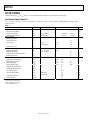
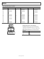
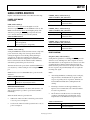
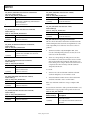
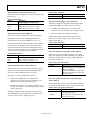
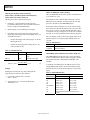
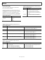
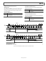
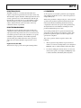
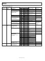
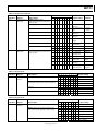
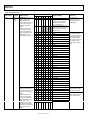
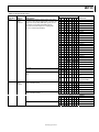
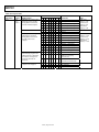
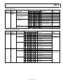
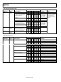
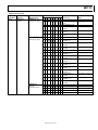
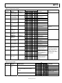
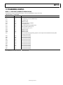
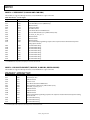
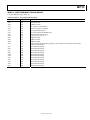
Table 174. Register 0x04
Bit
Subaddress
0x04
Register
Extended
Output
Control
Bit Description
RANGE. Allows the user to select
the range of output values. Can
be BT656 compliant, or can fill the
whole accessible number range.
7
6
5
4
3
2
1
0
0
1
Register
Setting
16 < Y < 235,
16 < C < 240
1 < Y < 254,
1 < C < 254
EN_SFL_PIN.
0
1
SFL output is
disabled
SFL information
output on the
SFL pin
Comments
ITU-R BT.656
Extended range
SFL output enables
encoder and decoder to
be connected directly
During VBI
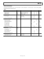
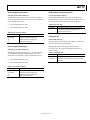
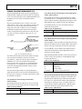
BL_C_VBI. Blank Chroma during
VBI. If set, enables data in the VBI
region to be passed through the
decoder undistorted.
0
1
Decode and
output color
Blank Cr and Cb
Controlled by TOD
TIM_OE. Timing signals output
enable.
0
1
HS, VS, F threestated
HS, VS, F forced
active
Recommended
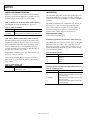
DR_STR[1:0]. Drive strength of
output drivers can be increased or
decreased for EMC or crosstalk
reasons.
0
0
1
0
1
0
1
1
Low drive, 1×
Medium-low, 2×
Medium-high,
3×
High drive, 4×
Reserved.
1
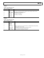
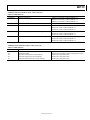
BT656-4. Allows the user to select
an output mode compatible with
ITU- R BT656-3/4.
0
1
Rev. B | Page 69 of 104
Set to default
BT656-3compatible
BT656-4compatible