1
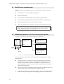
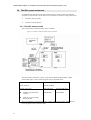
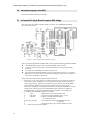
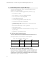
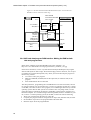
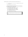
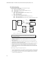
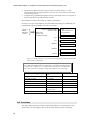
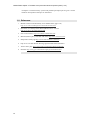
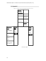
Mobile Robot chapter 3: The 8051 micro-processor based computer system (v.4.a) Chapter 3:The 8051 Micro-controller based computer system Objectives ! Study the structure of an 8051 micro-controller based system ! Study the internal memory model of the 8051 ! Study the external memory interfacing architecture to enable on-line software system development. ! Study addressing methods for interfacing various input/output peripheral devices of an 8051 based system. 3.1 Introduction In this chapter we discuss the structure of a micro-controller unit (MCU) based system that will be used to build our applications. We will first talk about why we choose the 8051 as our processor and we will introduce the 8051 family members and their differences. Then we will discuss the fundamentals of the 8051 processor. In particular we will discuss the memory model, the internal registers and their usage. Then we will discuss in detail the design of the 8051 single board computer (SBC), which is the heart of our robot system. Finally we will talk about the peripheral chips of our system and their functions. 3.2 Micro-controllers: Why? What? How? So, why do we use a micro-controller for the soul of our robot and other applications? It is simply because micro-controllers are cost effective and small enough to fit into our design. In fact micro-controllers are so common that it can be found in washing machines, microwaves, motor cars, or even inside you Octopus smart card. So the next question is what type of micro-controller should we use? We chose the 8051 because of its popularity and cost effectiveness. Moreover there are plenty of public domain software as well as commercial libraries available in the industry. The 8051 (or the ROM-less version 8031) is originally an Intel product [1], a cousin of the 80X86 family designed for the embedded control market in the 80s. As popular standards especially software standards don’t easily die down, it flourishes for years and becomes one of the most popular 8-bit micro-controllers worldwide. It was in the 90s that some other companies jumped into the bandwagon and built faster and more complex micro-controllers based on the 8051 core. That means the whole library of 8051 assembly code can be reused. The representatives of such products are flash based Amtel 8951 [7] and the Philips XA (16-bit extended architecture) micro-controllers [5]. They can run as fast as 30MHz and the Philips XA even has a small network standard (Controller Area Network CAN) [5] of its own for inter-micro-controller 1 Mobile Robot chapter 3: The 8051 micro-processor based computer system (v.4.a) communications – a microwave oven can talk to a refrigerator etc. The limitation is therefore left for designers’ imaginations. In our discussion will still use the humble 8051 –the core design common to all members. Nevertheless, the system developed can be upgraded later to use other faster and powerful processors of the family with minimum modification of the software drivers. So what exactly is a micro-controller? In fact it is a full functional computer on its own, hence it is also called a single-chip-computer meaning it can compute and think by itself. A typical micro-controller (e.g. 8051) may have the following modules. ! CPU (Central Processing Unit) ! Some internal data Ram (e.g. 128 byte) and a few (e.g.4~8) kilobytes of program ROM. ! Hardware interrupt mechanisms (e.g. 5 different interrupt sources). ! Parallel (e.g. 24 bits) input/output bus so that it can communicate with the outside world. ! A serial input/output so that it can make more distant communications with other computers. ! Timers for counting or generating exact timing output signals for control purposes. ! Power down circuit to keep the internal data even the main power is cut off. When it happens, the internal data ram can be supported by a small rechargeable battery. When the main power comes back, the rechargeable battery is recharged again for the next power failure. This feature is essential used to maintain continuous service when the power may be cut off occasionally. Figure 3. 1 This is the 8051 pin assignment diagram, from [1]. Exercise3.1: Discuss the differences between the two terms: microcontroller and microprocessor. 2 Mobile Robot chapter 3: The 8051 micro-processor based computer system (v.4.a) 3.3 The 8051 micro-controller family All have 128 bytes internal RAM, 2 timers, 32-bit parallel IO, serial IO, 5 interrupt sources ! 8031: ROM-less ; use external ROM for programs ! 8051: 4K-byte ROM ! 8751: 4K-byte UV-EPROM (ultra-violet erasable, re-programmable) ! 8951: 4K-byte [7] (Flash-ROM-based, Electrical erasable, re-programmable) ! Philips extended Architecture (16-bit with AD converter) ! 8X52: An extended member, which has 256 bytes internal RAM and 3 timers. Exercise3.2: Search another 8-bit MCU (e.g. MC68HC11 or Z84) on the Internet, discuss and compare it with the 8051 in terms of (a) maximum speed, (b) memory size and (c) interrupt features. 3.4 Fundamental operations of a micro-controller based system. A typical micro-controller system has the following configuration. Clock oscillator i.e. 11.0592 Mhz Micro-controller e.g. 8051 RAM for data and program /reset ROM for storing startup program Reset switch GND Peripheral IO devices, e.g. 8255, 8253 realtime-clock, etc. Figure 3. 2 A typical micro-controller system Every microprocessor system has a similar startup and operating procedure, which is depicted below. 3 ! The microprocessor is connected to a clock, which determines the operating frequency of the system, and a reset switch that starts the program from a reset location. Our system uses a clock of 11.0592 MHz, it is the basic clock for generating memory read/write cycles, baud rate for the serial port and the main clock of the internal timers. ! After the reset switch is depressed, the microprocessor first loads the content of a startup location from the startup ROM (e.g. 0000Hex for 8051). ! Then it executes the content of the startup program; usually it is a long jump to the ROM space for the starting point of the booting program, says the boot loader. Mobile Robot chapter 3: The 8051 micro-processor based computer system (v.4.a) 3.5 The 8051 system architecture To understand the operation of the 8051 based system, we need to study how data and programs are stored in the system. Here we will examine two memory storage subsystems: " The 8051 memory model " The 8051 internal registers 3.5.1 The 8051 memory model This is the memory model of an 8051 micro-controller. Figure 3. 3 memory model of an 8051 micro-controller The 8051 memory model has 3 parts (A) the internal RAM inside the MCU, (B)the external data space (c) the external program space as depicted below. Internal address (RAM) in Hex External address space in Hex inside the MCU outside the MCU 00->FF (128 bytes) Data 64K bytes Program 64K bytes ! 80#FF (special function registers 0000#FFFF 0000#FFFF ! 00# 7F (4 register banks R0,R1,R2,R3) The lower addresses of the internal RAM , contain 4 data register banks (R0,R1,R2,R3) for the program to store temporary data. 4 Mobile Robot chapter 3: The 8051 micro-processor based computer system (v.4.a) The upper internal RAM contains the Special Function Registers (SFR) for storing various operating data (e.g. program counter, stack address registers etc.) for the MCU. They can be accessed by the direct addressing method -- ‘mov’ instructions. The external data memory can be accessed by the ‘movx’ instructions. The external program memory is used to store programs. Table 3. 1 internal RAM usage and Special Function Register SFR map[1 ] Address location (H=hex) Content 80-FFH Special function registers (SFR) 30-7FH (64 bytes) Scratch pad area for stack 20-2FH (128 bits) Bit addressable segment 18-1FH (8 bytes) R0-R7 bank3 10-17H (8 bytes) R0-R7 bank2 08-0FH (8 bytes) R0-R7 bank1 00-07H (8 bytes) R0-R7 bank0 You will find this table useful when we talk about the programming of the 8051 in later chapters. Erecise3.3: Guess what are ACC, SP in the above table? Exercise3.4: What assembly instruction should you use to access the value of IP? Exercise3.5: What assembly instruction should you use to access the value of external RAM location 2345H? Exercise3.6: Under what circumstances should program memory location 9256H be accessed? 5 Mobile Robot chapter 3: The 8051 micro-processor based computer system (v.4.a) 3.6 Assembly language of the 8051 Learn this from the textbook you brought. 3.7 A simple 8051 Single Board Computer SBC design Now let us look at a simple computer based on an 8752 (UV-EPROM based 8052) micro-controller device. Figure 3. 4 An 8752 based microcomputer from [8] This is a small Single Board Computer SBC system with the following hardware modules. ! One 8K data RAM (6264), one 4-K program ROM inside the 8752. ! A simple resistor-capacitor (RC) circuit to pull down the reset pin (pin 9) after power up. ! A Crystal of 11.0592MHZ is connected to pin 18,19. ! Serial interfaces MAX232 (RS232 to TTL level interface) at pin 10,11. Note that RS232 uses -12V and +12V to represent low and high, while TTL uses 0 and 5V to represent low and high, respectively. First let us look at what the 8051 system will do after reset. • Power-up or reset. After power up or when the reset pin 9 is at ‘high’ for about 1ms (if the master clock is 10MHz or over as discussed in the data book of 8752), the system is being reset. Then the 8051 will fetch its first instruction from the ROM space at address 0000H. Special care must be taken when you write the first instruction. Usually it is a long jump instruction to the system initialization such as setting up the system clock, serial communication link with a host computer or loading the start up program from flash memory to RAM (i.e. boot loader) etc. • A simple startup assembly segment is as follows: 1 Org 0 ; 0000H is the first instruction after reset 2 ljmp start ; long jump to the line labelled ‘start’ --line 6 3 Org 30h ; arbitrary, but addr. 0003H~002FH 5 ; are reserved for stack 6 start: mov sp,30h-1 ; set stack point at 30h (internal RAM, max size 7 is 64 bytes) 8 ; the stack will grow up to the max address of 7FH 9…. Other start up program segment 6 Mobile Robot chapter 3: The 8051 micro-processor based computer system (v.4.a) Exercise3.7 The R,C connected to the reset (pin9) of the MCU is 4.7K and 10uF respectively., explain the choice of these values. Exercise3.8 Describe how to modify the hardware circuit to have a 32Kbyte RAM. You should first determine the pin number s of the 32K-RAM and see how it is connected to the system. Exercise3.9: In the above start-up program, why does sp = 30h-1 not 30h? What does tell you about the stack operation of the MCU? • The 8051 has 128 bytes of internal RAM for storing working data such as the stack and variables. But if that is too small for your program, you can use the external data RAM 6264 attached (0000H - FFFFH) to the 8051. The assembly instruction for external RAM read/write is “movx”. Now it turns out it is not a single chip system after all. A basic system would at least have a minimum set of electronic circuit. For example, a circuit to turn the action of pressing of a button into a 1ms high pulse signal (reset signal). Also some circuits are needed to connect the 8051 to a ROM for storing program and RAM for storing data. (In fact if you use the 8051 version of the 8051 family, it has a built-in 4K ROM for storing start up and necessary programs; or for the case of the 8951, which has 4K electrical programmable Flash ROM for program development purpose). Exercise3.10: State the differences among 8031, 8051 and 8951. Explain how to enter a program to an 8951? Exercise3.11: The internal RAM has addresses 00#FFH, and the external data RAM also has that same addresses, will it create a conflict? (Answer in terms of hardware and software aspects). 3.8 8051 memory interface Diagram from http://www.pjrc.com/tech/8051/pm2_docs/hardware.html The 8051 is designed for small systems, in order to reduce the number of pins used, time multiplexing of signals is used. For example, port 0 and p2 are used as input/output ports or memory interface pins. Here we will study the memory interface methods and see how they perform during memory read/write. The three topics that we will discuss and their related hardware pins are as follows: (1) Address and data bus time-multiplexing for external memory devices (2) External Program memory read: Hardware pins involved: port 0 and port 2 (P0.1~P0.7, P2.1~P2.7 = 16 bits), and /ALE, /PSEN (3) External Data memory read/write: Hardware pins involved: port 0 and port 2 (P0.1~P0.7, P2.1~P2.7 = 16 bits), and /ALE, /PSEN, /RD, /WR 3.8.1 Address and data bus time-multiplexing for external memory devices As discussed before an 8051 has 4K internal ROM to store programs. But if we use the 8031 version (or if you want to have a program longer than 8K) we need to ask the 8031 to access external ROM. Note that when pin31 (/external enable /EA) of an 8051 is grounded, it will ignore the internal ROM and use the program from external ROM; it will be treated exactly as an 8031. Alternatively, if pin31 is connected to 5V, the 8051 will read programs from the internal ROM. 7 Mobile Robot chapter 3: The 8051 micro-processor based computer system (v.4.a) Let us examine the circuit diagram and see how a ROM memory chip is connected to the 8031. The ROM device is 270251, which is a 64K = 216bytes (with 16 address pins) ROM. To save the number of pins we see that the 8031 micro-controller uses a technique called time multiplexing, it multiplexes data and address bus together. For a 64K-byte ROM, it needs 16 bits address and 8 bit of data, so a total number of 16+8=24 bits are required. However, by multiplexing the two sets of signals together we can save 8-bit of signals so as to reduce the size of the bus. To achieve this goal an additional device, an external device -- 8-bit latch, is needed to hold the address bits when they appear when ALE is high and use it later on, we see how it woks in the following diagrams. ALE /PSEN PORT0 PORT2 Figure 3. 5 External program memory read interface block diagram and timing diagram 3.8.2 External Program MEMORY (ROM) interface The timing diagram is shown above. When the 8031 wants to read program code from external memory, it acts as follows: ! It first sets up ALE (address latch enable) and /PSEN (program access enable) to high. ! The 8031 outputs address bits A0-A7 at port0(P0.0-P0.7) and outputs A8-A15 at port2 (P2.0-P2.7). ! Then the 8031 resets ALE to 0 to signal to the outside circuit that address bits at port0 are needed to be latched. ! An 8-bit latch, usually a 74373, with latch input (LE) connected to ALE will do it fine and the address bits a0-A7 are latched at the outputs of the latch 74373. ! Also /PSEN (program store enable) is reset to 0, as an effect, the ROM responses to give the data stored at the address pointed by A0-A7 & A8-A16 to the data bus connected at P0. ! The 8031 at this stage will read (latch) the data inside at the rising edge of /PSEN through the port P0. 8 Mobile Robot chapter 3: The 8051 micro-processor based computer system (v.4.a) 3.8.3 External Data Memory (RAM) interface The standard memory read procedure would now be explained. The configuration is very similar to program read, instead of using /PSEN for accessing the ROM, it uses /RD and /WR to access the RAM. As you may aware that RAM is “read” and “write” allowed, therefore two pins are designated for data memory interface. Here are the block diagram and the timing diagram. As you can see address/data time multiplexing is also used here. ALE /PSEN /RD PORT0 PORT2 ALE /PSEN /WR PORT0 PORT2 Figure 3. 6 External data memory read interface block diagram and timing diagram 9 Mobile Robot chapter 3: The 8051 micro-processor based computer system (v.4.a) 3.9 The 8031RL Single Board Computer SBD Design We now uses a SBC called 8031RL, which is versatile and cost effective design to illustrate the design of a typical system. (See http://www.cse.cuhk.edu.hk/~khwong/ceg3430/8031rl_schematic_vert.jpg) " Has an 8031 micro-controller. " Power management circuitry to cope with power down failure. " One 8~32-Kbyte (6764 or 67256) startup ROM " One data 32-Kbyte SRAM (62256) " One 32-Kbyte data/program SRAM ((actually 24K is usable) " Two 8255 parallel interface chips, totally 48 IO bits " One real-time clock DC1287 with internal battery for keeping system time and generation of interrupt clock. " RS232 interface to PC through a converter chip MAX-232. " Watch dog timer MAX691. " A full bridge rectifier circuit and a power stabilizer 7805 for accepting 7~9V AC or DC power supply. " LCD interface to a standard 20x2 LCD panel. 3.9.1 8051 and external memory interfaces We will first start to discuss the interface between the program Rom and the data RAM. Then we will talk about how to make RAM used as both program and data store. Recall again the 8031 has three external memory read/write operations. Table 3. 2 8051 external memory read/write operations /PSEN /RD /WR (1) External program read 0 1 1 (2) External data read 1 0 1 (3) External data write 1 1 0 3.9.2 8051 and external program ROM (UV-EPROM) interface Our system uses a UV-EPROM (or called EPROM, U5 in the 8031RL schematic) as the read only memory store to hold the startup program. The circuit is a straightforward one and requires the 74373 to latch the address, and the ALE of 8031 is connected to latch input (LE) of 74373. The system uses a programmable array logic circuit (GAL) 18CV8 for address decode. So that if necessary one can change the address map by changing the content of the GAL chip. The connections are as follows: 10 Mobile Robot chapter 3: The 8051 micro-processor based computer system (v.4.a) ! /PSEN (Program enable select) of 8031 is connected directly to the /OE of the EPROM. Therefore only external program can be read from this EPROM. Since it is an 8031 (same as 8051 with pin /EA=0) chip so no programs would be found within the MCU, all programs should be stored externally. ! The address decoder output for the range 0000-7FFFH is connected to the /CE of the EPROM. We see that upper address lines (A14,A15) are used for address decode to point to the EPROM chip. And lower address lines (A0-A13) are used to address to memory addresses within the memory chip. Figure 3. 7 An 8031 and UV-EPROM 27256 interface 8031 MCU /EA A15, /PSEN /RD,/WR ALE P00-P07 (A0A7)/ (D0-D7) Address/dat multiplexed 0000-7FFFH program read select /output Address decoder 18CV8 LE 74373 latch P20-P26(A8-A14) /PSEN 32K-byte EPROM 27256 /CE A0-A7 D0-D7 A8-A14 /OE 3.9.3 8051 and external data RAM interface Our system uses an SRAM 62256 (U6 in the 8031RL schematic) as the data memory store. The circuit is a similar to the MCU-EPROM circuit, which also requires the 74373 to latch the address. The ALE of 8031 is connected to latch input (LE) of 74373. And the system uses a programmable array logic circuit (GAL) 18CV8 for address decode. So that, if necessary, one can change the address map by changing the content of the GAL chip. The connections are as follows: 11 " A15 of the 8031 is connected to /CE of the SRAM through a MAX691 watch-dogtimer chip. Let’s forget about the special functions of the MAX691 (its function will be explained later) and treat it as a direct connection. Therefore whenever A15=0, the address is within 0000-7FFFH, the memory chip is selected. The read/write operations are now coordinated by /RD and /WR of the 8031. " /RD (pin17 of 8031), /RW (pin16 of 8031) are connected to /RD (pin 22 of 622256) and /WR (pin 27 of 62256), respectively. Since during external program read as discussed above in Table 3. 2, /RD and /WR are high, therefore only external data read/write instructions can read/write this SRAM. " As a conclusion, this SRAM will only used for external data storage. Mobile Robot chapter 3: The 8051 micro-processor based computer system (v.4.a) Figure 3. 8 An 8031 and External Data SRAM 62256 interface.** Note that treat MAX691 as direct connection at this stage 8031 MCU /EA A15, /PSEN /RD,/WR ALE P00-P07 (A0A7)/ (D0-D7) Address/dat multiplexed P20-P26(A8-A14) /RD /WR 0000-7FFFH external data RD/WR select /output Address decoder 18CV8 Max 691 LE 74373 latch 32K-byte SRAM 62256 /CE A0-A7 D0-D7 A8-A14 /OE /WR 3.9.4 8051 and data/program RAM interface: Making the RAM as both data and program store (Refer to the schematic of the 8031RL SBC from cache computer), see http://www.cse.cuhk.edu.hk/~khwong/ceg3430/8031rl_schematic_vert.jpg In the above discussion, we have a system that has 64 Kbytes ROM space for program and also 64K bytes for data storage. We should be happy about it. However, this set-up is not suitable for program development, why? Since you need to develop the program in the hard way, such as. " Use a PC to write your program. " Make UV-EPROM (or ROM) that has the object file (or machine code) or the program " Insert the ROM into the circuit board. The main problem is, programming the UV-EPROM once will take 10 minutes, and it is too long for a debug cycle. So the ideal way is to have an operating System (O.S.) sitting on the SBC, and a user is able to write program, run it and debug it interactively with the operating system. But our SBC system is too small to have everything inside, so some people developed a scheme for developing a small SBC system with the assistance of a Personal Computer. It is a method using a monitoring ROM (similar to the BIOS of your PC, in fact it is a small operating system) in the SBC, which looks like the following. 1. Write your program using the editor on a host PC. 2. Compile your program in the PC and generate an object file (machine code) for 8051. 3. Download the object file to the program RAM of the 8051-SBC 4. RUN the object file at the program RAM. 12 Mobile Robot chapter 3: The 8051 micro-processor based computer system (v.4.a) Figure 3. 9 Software development using monitor ROM To have the above scheme we need two important things: 1. A program at the ROM for monitoring the 8051 system, it should be able to communicate with a host PC computer and download object file form the PC to local RAM and run the program there. Thus this program at ROM is called a monitor program. 2. A shared RAM space for holding program and data simultaneously, in this light we have the design shown below. Figure 3. 10 Memory architecture showing external shared program and data RAM One way to have this development system is have a program ROM at 0000-7FFFH to store your monitor program (a simple operating system), data RAM at 0000-7FFFH for storing variables and your working data. It is noted that even the address is the same as the program space, it doesn’t matter, since program and data are separate entities and differentiable by the hardware signals /PSEN (for retrieving programs) and /RD, /WR (for read, write data reps.). The most important part is a program/data shared RAM at 8000-FFFFH for storing data and at the same time for saving programs for testing. It is interesting to see that this RAM space can be used for both purposes, such that: ! It is treated as data store when the 8031 executes external data read/write instructions to access data in this address range. 13 Mobile Robot chapter 3: The 8051 micro-processor based computer system (v.4.a) ! It is treated as program store when the 8031 is reading program instructions within this address range. So how to design a circuit to have such functions? It is done by a careful design of the chip select decoder for the /CS and /OE pins of RAM and ROM devices using the following rules: ! ROM1: Program retrieval, /PSEN=0; address range is total 16-bit (64K bytes) ! RAM1 for data only (range 0000-7FFFH): $ Data memory read: /RD = 0, /WR = 1, /PSEN = 1 $ Data memory write /RD = 1, /WR = 0, /PSEN = 1 ! RAM2 (for data and program, range 8000-FFFFH): $ Data memory read: /RD = 0, /WR = 1, /PSEN =1 $ Data memory write: /RD = 1, /WR = 0, /PSEN =1 $ Program memory read: /PSEN =0 $ Program memory write : never happen Exercise3.12 When will an 8051 read in instructions, from where, and how? Exercise3.13 What 8051 signals are involved during (1) data write, (2) data read? 14 Mobile Robot chapter 3: The 8051 micro-processor based computer system (v.4.a) 3.9.5 Address decoding So this is the decoding table used in the 8031RL SBC computer: (* is logical AND, + is logical OR) ! ROM1 (0000-7FFFH) 32K program ! /CE A15 (for all addresses 0000-7FFFH has A15=0) ! /OE /PSEN ! RAM1 (0000-7FFFH) data only $ /CE A15 (for all addresses 0000-7FFFH has A15=0) $ /WR /WE of 8031 $ /OE /RD of 8031 ! RAM2 (8000-FFFFH) program data shared $ /CE /A15 (for all addresses 8000-FFFFH has A15=1) $ /WR /WE of 8031 $ /OE /PSEN and /RD (either data read or program read will get output) 8031 Decoder PEEL GAL 18CV8 A15 /A15 A15 /WR /RD /WR /PSEN /PSEN and /RD /CE /OE /OE A15 /CE 00007FFFH RAM1 /WR /RD /WE /OE 00007FFFH ROM1 /PSEN /CE 8000-FFFFH RAM2 /WE Figure 3. 11 Address decoder and memory devices Exercise3.14 Redesign the above circuit so that we only use address space 8000-DFFFH of SRAM2. 1. 2. 3. 4. 5. In practice, the operating system (or monitor program) will be in ROM1. The development cycle is: At power up, it will enable a serial communication link with a terminal (Windows Hyper terminal etc). A programmer will develop his program on the PC using a cross compiler of C and generates 8031 executable code (object code). Then under the instruction of the developer using the monitor program it can delivery the object code to the space starting at 8000H as if it is writing data to this space. Finally the developer issues a run-from-8000H command to the monitor program at the 8031–SBC and the 8031 will execute from that location which is the object code he/she is testing. The advantage of using this development system is: • • 15 The development hardware is very minimal: a single chip computer, a PC and a serial cable, no need for an In Circuit Emulator, which is an expensive piece of equipment. Turn around time is fast, there is no need to blow an EPROM (may take 10 minutes or more) for a development cycle. Mobile Robot chapter 3: The 8051 micro-processor based computer system (v.4.a) • • The monitor program at the 8031 can provide the necessary library, i.e. serial interface drivers for the target program to call from. It is in fact akin to system calls of an operating system. It supports any programming languages as long as the output of the cross compiler at the PC is the object code understood by the 8031. We will discuss it more in the chapter on software development. In order to save space and complexity the whole address-decoding job is handled by the programmable logic device PEEL GAL 18CV8 as follows. A10-A15, /PSEN, /RD,/WR of 8031 /range of (8000-DFFFH) /PSEN or /RD PEEL GAL 18CV8 used as address decoder A15 A15 /E00XH /E80XH /F8XX /CS /OE of RAM2 (U7) Program/data /CS of RAM1(U6) /CS of ROM1(U5) /CS of 8255-U9 /CS of 8255-U8 LCD Figure 3. 12 Address decoder circuit and truth table, diagrams are from the 8031RL SBC manual from Cache computer. Exercise3.15 Write the Logic formulas of the decoding circuit in term of A0A15, /RD, /WR, /PSEN whichever applicable. Use loosely decoding method to reduce the complexity, i.e. you don’t need to decode the exact locations. The result would be acceptable as long as the addresses do not overlap. External address range Program 0000-7FFFH Device and pin name /CS of ROM1 Data 0000-7FFFH /CS of RAM1 Data 8000-Data DFFFH /CS of RAM2 Data E000-E003H /CS of 8255-U8 Data E800-E803H /CS of 8255-U9 Data EC00-EC0D /CS of DS1287 real time clock Data F000-F002H /CS of LCD Formulas Table 3. 3 Input/output peripheral devices address map 3.10 Conclusion The design and functioning of an 8031 single board computer are discussed in this note. In particular, basic knowledge of how to use the 8031 internal registers, interfacing 16 Mobile Robot chapter 3: The 8051 micro-processor based computer system (v.4.a) techniques to external memory systems and parallel input/output pins are given. Various hardware development techniques are mentioned. 3.11 References: 17 1. MCS® 51 Microcontroller Family User's Manual from (page 1-50) http://www.intel.com/design/mcs51/manuals/272383.htm 2. Data sheet of a 32K-byte Static RAM (SRAM) device 76C256 http://www.skt.co.kr/gm76c256clcll.pdf 3. 8031 serial interface http://www.8052.com/8051ser.htm 4. Manual (8031m7.pdf ) of 8031RL SBC from http://www.cachecom.com/ 5. Philips MCU home page http://www.semiconductors.com/mcu/ 6. http://www.cse.cuhk.edu.hk/~khwong/ceg3430.htm#Useful information 7. Amtel’s 8951 page: http://www.atmel.com/atmel/products/prod20.htm 8. Paulmon http://www.pjrc.com/tech/8051/pm2_docs/hardware.html Mobile Robot chapter 3: The 8051 micro-processor based computer system (v.4.a) 3.12 Appendix 1 Figure 3. 13 Address map of the 8031RL-SBC all addresses are in hex. External RAM2 and IO addresses F000-F002 LCD (con2) EC00-EC0D /CS of DS1287 real time clock E800-E803 8255(U8) E000-E003 8255 (U9) 8000-DFFF External RAM2 62256 (U7) Internal RAM of 8031 External External data RAM1 Special function registers, SFR (80FF) 0000- Stack IC=62256 (30-7F) (U6) Program ROM1 0000- 7FFFH 7FFFH IC=27256 (U5) Bit addressable segment (20-2F) 128 bytes RAM (00-1F):4 registers banks RB0,1,2,3 -- End of this chapter -- 18 Mobile Robot chapter 3: The 8051 micro-processor based computer system (v.4.a) 19