1
Application Note AN9997
GORE QUIETZONETM CABLES
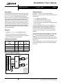
PATTERN GENERATOR
ISL5x29 EVALUATION BOARD
2x20 PIN HEADER
2x20 PIN HEADER
8-14 BITS
SMA
CABLE
1/2 ISL5x29
DAC
8-14 BITS
SPECTRUM ANALYZER
1/2 ISL5x29
CLOCK
OPTIONAL
DIRECT CLK
CABLE
50Ω
DAC
+3.3V
POWER
SUPPLY
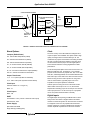
FIGURE 1. INTERSIL ISL5x29 EVALUATION SYSTEM SETUP BLOCK DIAGRAM
Board Options
Clock
Jumpers (Default State)
The clock circuitry on the ISL5x29eval1 is designed for a
couple of options to be available. One option allows a high
quality clock signal to be connected directly to J2. The
combination of jumpers and resistors surrounding J2 allows
the user to create a 50Ω power splitter so the same clock
can be fed off the board (J22) to clock the digital pattern
source without reflections causing degradations in DAC
performance.
J19 - Selects DAC Sleep Mode (OPEN)
J21 -Selects External Reference (OPEN)
J20 - Selects Internal Reference (SHORT)
J17, J5 - Selects IOUTA, QOUTA (SHORT)
J15, J4 - Selects IOUTB, QOUTB (SHORT)
J8, J14 - Grounds the Transformer Output (SHORT)
J23-J27 - Selects Clock Path and Termination
Output Transformer
T1, 4 - T1-1T (case style Mini-Circuits KK81)
T2, 3 - ADT1-1WT (case style Mini-Circuits CD542)
Clock Input
2x20 Pin Headers J1 or J3 (pin 19)
SMA - J2
Clock Output
To use the 50Ω power splitter connect the clock source to J2.
Make sure that R16, R31, and R32 are ~17Ω. Populate
jumpers J24 and J25. Do not populate J23, J26, or J27. With
C20, R47, and R48 populated, the clock will be biased at the
DAC clock input, so the clock source does not have to be DC
biased. If using J2 as the clock input but not using J22 to
clock an external device, populate jumper J27 so the
impedance of the power splitter is maintained.
Another option is to bring the clock on the board via the
ribbon cables. Choose pin 19 of J1 or J3, but not both.
Populate the necessary jumper to connect pin 19 to the DAC
clock input (J23 if via J1 or J26 if via J3). Do not populate
J24 or J25 (unless 50Ω termination is desired).
SMA - J22
Digital Inputs
RSET
Fixed Resistor - R91 (1.91kΩ = 20mA full scale output)
Potentiometer - R90
Power SupplySplit AVDD and DVDD
Single VDD (by installing R63)
2
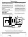
The digital inputs are expecting 3V CMOS levels in offset
binary format. The board is shipped without termination
resistors so that most systems can drive the load. The board
is configured so the user can populate 50Ω termination
resistors if required. Consult the datasheet for the DAC for
min/max amplitude requirements for the clock and data.