1
Application Note AN9997
Analog Outputs
The transformer configuration is such that it expects to see a
50Ω load at the end of an RF cable. If the user wishes to
evaluate the single-ended performance of the DAC, J6/J7
and/or J16/J18 will need to be populated, R73, 74, 79, and
80 should be populated with 50Ω resistors, and R69, 71, 76,
and 77 should be removed to eliminate the transformer and
differential resistor from the circuit. Other loading can be
considered so long as the combination of the output current
and output resistance does not violate the output voltage
compliance range.
Board Schematics/Layout/BOM
The schematics, board plots, and bill of materials can be
downloaded from the Intersil website. Search on the DAC
part number using the Part Search.
ISL5x29 + ISL5217
The ISL5x29 evaluation board is designed to interface
directly to an ISL5217 evaluation board. The ISL5217 is an
Intersil 104MSPS Digital Up Converter (DUC). The ISL5217
can be used to generate 1–4 narrowband carriers or 1–2
wideband carriers. Consult the ISL5217 documentation for
detailed information on using the ISL5217EVAL.
Using short ribbon cables, connect J3 and/or J4 on the
ISL5217EVAL (DUC) to J1 and/or J3 on the ISL5217EVAL
(DAC). These ribbon cables connect the digital outputs of
the ISL5217 to the digital inputs of the ISL5929.
To provide a common clock signal for the boards, remove
oscillator U6 from the DUC board and connect an RF cable
from J11 of the DUC board to J22 of the DAC board.
(Sometimes the length of the cable has to be adjusted to
achieve adequate setup and hold times between between
DATA and CLK.) For the DAC board, jumpers J23, J26, and
J27 are not populated. The clock source should be
connected to J2 on the DAC board by an RF cable. On the
ISL5217EVAL, verify the jumper from JP5 pin 2 to JP5 pin 3
is installed. Also install a jumper from JP5 pin 1 to JP6 pin 1
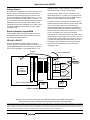
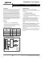
to provide 50Ω clock signal termination. See Figure 2 for a
block diagram of the two boards connected. Consult the
schematic for the ISL5217EVAL for more information
regarding the DUC.
RF CABLE
CLOCK IN (104MSPS MAX)
J11
50Ω
SMA
CABLE
J2
RIBBON CABLES
J22
2x20 PIN HEADER
2x20 PIN HEADER
2x25 PIN HEADER
ISL5217
4CH DIGITAL
UP CONVERTER
2x25 PIN HEADER
14 BITS
TO SPECTRUM
ANALYZER
1/2 ISL5929
DAC
14 BITS
CLOCK
1/2 ISL5929
DAC
ISL5x29 DAC EVALUATION BOARD
+3.3V (<0.25A)
+5V (<2A)
ISL5217 DUC EVALUATION BOARD
POWER
SUPPLY
POWER
SUPPLY
FIGURE 2. INTERSIL ISL5929 + ISL5217 SETUP BLOCK DIAGRAM
All Intersil U.S. products are manufactured, assembled and tested utilizing ISO9000 quality systems.
Intersil Corporation’s quality certifications can be viewed at www.intersil.com/design/quality
Intersil products are sold by description only. Intersil Corporation reserves the right to make changes in circuit design, software and/or specifications at any time without
notice. Accordingly, the reader is cautioned to verify that data sheets are current before placing orders. Information furnished by Intersil is believed to be accurate and
reliable. However, no responsibility is assumed by Intersil or its subsidiaries for its use; nor for any infringements of patents or other rights of third parties which may result
from its use. No license is granted by implication or otherwise under any patent or patent rights of Intersil or its subsidiaries.
For information regarding Intersil Corporation and its products, see www.intersil.com
3