1
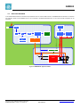
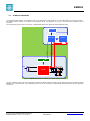
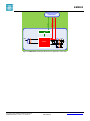
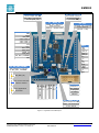
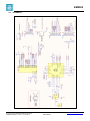
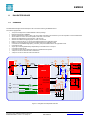
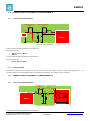
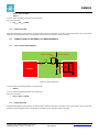
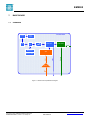
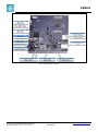
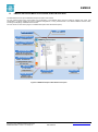
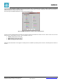
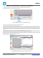
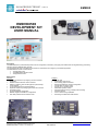
EM8500 6. DAUGHTER BOARD 6.1. OVERVIEW The EMDVK8500 daughter board development kit is the board containing the EM8500 device. The board is equipped with: The power management controller EM8500 in MLF24 package External components for EM8500 Specific measurements nodes on HRV, LTS, STS, VSUP and VAUX to be measured by the A/D acquisition unit of the Base Board Shunt resistors to monitor the current profiles of the HRV, LTS and STS. Switches to independently connect the HRV, LTS and STS. Switches to enable some discharge path on HRV, LTS and STS Relays to select the SPI or I2C coming from the Base Board or the Application board. Relays to connect the wake-up input from the Base Board or the Application board. Connections to the EM8500 flags (HRV_LOW BAT_LOW) to the Base Board or the Application board. Connection to HRV. Super cap and rechargeable battery independently connectable to the LTS output Connection to external LTS Connection to external STS and spare footprint for additional STS capacitor Jumper to connect or disconnect the LTS electronic Jumper to connect or disconnect the STS electronic A/D HRV 0.2Ω shunt 0.2Ω shunt A/D LTS 2Ω shunt J102 U101 User HRV CN101 LX1 CN102 2Ω shunt CN103 LTS VDD_LTS CN104 VDD_HRV Q101 J105 U103 R111 J106 SuperCAP Q102 EM8500 Q103: B 2Ω shunt +USB A/D STS CN106 User LTS J103 J101 Battery STS VDD_USB VDD_STS I2C SPI APPLICATION I2C - SPI BASE BOARD RL101-103 WAKE APPLICATION BASE BOARD UP BASE BOARD APPLICATION BASE BOARD FLAGS APPLICATION WAKE_UP VSUP BAT_LOW HRV_LOW VAUX2 VAUX1 VAUX0 Q103: A User STS C112 A/D A/D VSUP A/D VAUX2 A/D VAUX1 VAUX0 CN107 CN105 VAUX_GND2 VAUX_GND1 VAUX_GND0 Figure 6-1: Daughter board simplified schematic Copyright 2015, EM Microelectronic-Marin SA EMDVK8500-MN01, Version 1.0, 29-Sep-15 22 PRELIMINARY www.emmicroelectronic.com