1
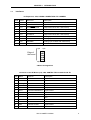
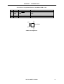
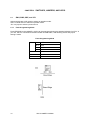
To our customers,
Old Company Name in Catalogs and Other Documents
On April 1st, 2010, NEC Electronics Corporation merged with Renesas Technology
Corporation, and Renesas Electronics Corporation took over all the business of both
companies. Therefore, although the old company name remains in this document, it is a valid
Renesas Electronics document. We appreciate your understanding.
Renesas Electronics website: http://www.renesas.com
April 1st, 2010
Renesas Electronics Corporation
Issued by: Renesas Electronics Corporation (http://www.renesas.com)
Send any inquiries to http://www.renesas.com/inquiry.
Notice
1.
2.
3.
4.
5.
6.
7.
All information included in this document is current as of the date this document is issued. Such information, however, is
subject to change without any prior notice. Before purchasing or using any Renesas Electronics products listed herein, please
confirm the latest product information with a Renesas Electronics sales office. Also, please pay regular and careful attention to
additional and different information to be disclosed by Renesas Electronics such as that disclosed through our website.
Renesas Electronics does not assume any liability for infringement of patents, copyrights, or other intellectual property rights
of third parties by or arising from the use of Renesas Electronics products or technical information described in this document.
No license, express, implied or otherwise, is granted hereby under any patents, copyrights or other intellectual property rights
of Renesas Electronics or others.
You should not alter, modify, copy, or otherwise misappropriate any Renesas Electronics product, whether in whole or in part.
Descriptions of circuits, software and other related information in this document are provided only to illustrate the operation of
semiconductor products and application examples. You are fully responsible for the incorporation of these circuits, software,
and information in the design of your equipment. Renesas Electronics assumes no responsibility for any losses incurred by
you or third parties arising from the use of these circuits, software, or information.
When exporting the products or technology described in this document, you should comply with the applicable export control
laws and regulations and follow the procedures required by such laws and regulations. You should not use Renesas
Electronics products or the technology described in this document for any purpose relating to military applications or use by
the military, including but not limited to the development of weapons of mass destruction. Renesas Electronics products and
technology may not be used for or incorporated into any products or systems whose manufacture, use, or sale is prohibited
under any applicable domestic or foreign laws or regulations.
Renesas Electronics has used reasonable care in preparing the information included in this document, but Renesas Electronics
does not warrant that such information is error free. Renesas Electronics assumes no liability whatsoever for any damages
incurred by you resulting from errors in or omissions from the information included herein.
Renesas Electronics products are classified according to the following three quality grades: “Standard”, “High Quality”, and
“Specific”. The recommended applications for each Renesas Electronics product depends on the product’s quality grade, as
indicated below. You must check the quality grade of each Renesas Electronics product before using it in a particular
application. You may not use any Renesas Electronics product for any application categorized as “Specific” without the prior
written consent of Renesas Electronics. Further, you may not use any Renesas Electronics product for any application for
which it is not intended without the prior written consent of Renesas Electronics. Renesas Electronics shall not be in any way
liable for any damages or losses incurred by you or third parties arising from the use of any Renesas Electronics product for an
application categorized as “Specific” or for which the product is not intended where you have failed to obtain the prior written
consent of Renesas Electronics. The quality grade of each Renesas Electronics product is “Standard” unless otherwise
expressly specified in a Renesas Electronics data sheets or data books, etc.
“Standard”:
8.
9.
10.
11.
12.
Computers; office equipment; communications equipment; test and measurement equipment; audio and visual
equipment; home electronic appliances; machine tools; personal electronic equipment; and industrial robots.
“High Quality”: Transportation equipment (automobiles, trains, ships, etc.); traffic control systems; anti-disaster systems; anticrime systems; safety equipment; and medical equipment not specifically designed for life support.
“Specific”:
Aircraft; aerospace equipment; submersible repeaters; nuclear reactor control systems; medical equipment or
systems for life support (e.g. artificial life support devices or systems), surgical implantations, or healthcare
intervention (e.g. excision, etc.), and any other applications or purposes that pose a direct threat to human life.
You should use the Renesas Electronics products described in this document within the range specified by Renesas Electronics,
especially with respect to the maximum rating, operating supply voltage range, movement power voltage range, heat radiation
characteristics, installation and other product characteristics. Renesas Electronics shall have no liability for malfunctions or
damages arising out of the use of Renesas Electronics products beyond such specified ranges.
Although Renesas Electronics endeavors to improve the quality and reliability of its products, semiconductor products have
specific characteristics such as the occurrence of failure at a certain rate and malfunctions under certain use conditions. Further,
Renesas Electronics products are not subject to radiation resistance design. Please be sure to implement safety measures to
guard them against the possibility of physical injury, and injury or damage caused by fire in the event of the failure of a
Renesas Electronics product, such as safety design for hardware and software including but not limited to redundancy, fire
control and malfunction prevention, appropriate treatment for aging degradation or any other appropriate measures. Because
the evaluation of microcomputer software alone is very difficult, please evaluate the safety of the final products or system
manufactured by you.
Please contact a Renesas Electronics sales office for details as to environmental matters such as the environmental
compatibility of each Renesas Electronics product. Please use Renesas Electronics products in compliance with all applicable
laws and regulations that regulate the inclusion or use of controlled substances, including without limitation, the EU RoHS
Directive. Renesas Electronics assumes no liability for damages or losses occurring as a result of your noncompliance with
applicable laws and regulations.
This document may not be reproduced or duplicated, in any form, in whole or in part, without prior written consent of Renesas
Electronics.
Please contact a Renesas Electronics sales office if you have any questions regarding the information contained in this
document or Renesas Electronics products, or if you have any other inquiries.
(Note 1) “Renesas Electronics” as used in this document means Renesas Electronics Corporation and also includes its majorityowned subsidiaries.
(Note 2) “Renesas Electronics product(s)” means any product developed or manufactured by or for Renesas Electronics.
User’s Manual
Release-it
TM
ZigBee -ready
Wireless Network Evaluation Board
Using the 78K0/KF1+ Microcontroller
Hardware Manual
Document No. U17586EE1V0UM00
Date Published June 2005
© NEC Electronics Corporation 2005
Printed in Germany
[MEMO]
2
UM U17586EE1V0UM00
•
The information in this document is current as of May, 2005. The information is subject to change
without notice. For actual design-in, refer to the latest publications of NEC Electronics data sheets
or data books, etc., for the most up-to-date specifications of NEC Electronics products. Not all
products and/or types are available in every country. Please check with an NEC Electronics sales
representative for availability and additional information.
•
No part of this document may be copied or reproduced in any form or by any means without the prior
written consent of NEC Electronics. NEC Electronics assumes no responsibility for any errors that may
appear in this document.
•
NEC Electronics does not assume any liability for infringement of patents, copyrights or other intellectual
property rights of third parties by or arising from the use of NEC Electronics products listed in this
document or any other liability arising from the use of such products. No license, express, implied or
otherwise, is granted under any patents, copyrights or other intellectual property rights of NEC Electronics
or others.
•
Descriptions of circuits, software and other related information in this document are provided for
illustrative purposes in semiconductor product operation and application examples. The incorporation of
these circuits, software and information in the design of a customer's equipment shall be done under the
full responsibility of the customer. NEC Electronics assumes no responsibility for any losses incurred by
customers or third parties arising from the use of these circuits, software and information.
•
While NEC Electronics endeavors to enhance the quality, reliability and safety of NEC Electronics
products, customers agree and acknowledge that the possibility of defects thereof cannot be eliminated
entirely. To minimize risks of damage to property or injury (including death) to persons arising from
defects in NEC Electronics products, customers must incorporate sufficient safety measures in their
design, such as redundancy, fire-containment and anti-failure features.
•
NEC Electronics products are classified into the following three quality grades: "Standard", "Special" and
"Specific".
The "Specific" quality grade applies only to NEC Electronics products developed based on a customerdesignated "quality assurance program" for a specific application. The recommended applications of an
NEC Electronics product depend on its quality grade, as indicated below. Customers must check the
quality grade of each NEC Electronics product before using it in a particular application.
"Standard": Computers, office equipment, communications equipment, test and measurement
equipment, audio and visual equipment, home electronic appliances, machine tools,
personal electronic equipment and industrial robots.
"Special":
Transportation equipment (automobiles, trains, ships, etc.), traffic control systems,
anti-disaster systems, anti-crime systems, safety equipment and medical equipment
(not specifically designed for life support).
"Specific":
Aircraft, aerospace equipment, submersible repeaters, nuclear reactor control
systems, life support systems and medical equipment for life support, etc.
The quality grade of NEC Electronics products is "Standard" unless otherwise expressly specified in NEC
Electronics data sheets or data books, etc. If customers wish to use NEC Electronics products in applications
not intended by NEC Electronics, they must contact an NEC Electronics sales representative in advance to
determine NEC Electronics' willingness to support a given application.
(Note)
(1) "NEC Electronics" as used in this statement means NEC Electronics Corporation and also includes its majority-owned
subsidiaries.
(2) "NEC Electronics products" means any product developed or manufactured by or for NEC Electronics (as defined
above).
UM U17586EE1V0UM00
3
4
UM U17586EE1V0UM00
NOTES
The information in this document is subject to change without notice. No part of this document may be
copied or reproduced in any form or by any means without the prior written consent of NEC
Engineering Ltd. and NEC Electronics Corp.
NEC Engineering Ltd. and NEC Electronics Corp. assume no liability for infringement of patents or
copyrights of third parties by or arising from use of a product described herein.
NEC Engineering Ltd. and NEC Electronics Corp. established proven quality assurance procedures
for all products manufactured by or on behalf of NEC Engineering Ltd. or NEC Electronics Corp.. As
part of product qualification process an intensive release test procedure has been established and
executed before the products are released for mass production and delivered to our clients. NEC
Engineering Ltd. and NEC Electronics Corp. would like to inform, that the standard quality assurance
procedure(s) have not been fully applied to this product and its documentation and that Neither NEC
Engineering Ltd. or NEC Electronics Corp. can assure the full and error free function and/or the
standard quality level.
CAUTION
This equipment should be handled like a CMOS semiconductor device. The user must take all
precautions to avoid build-up of static electricity while working with this equipment. All test and
measurement tool including the workbench must be grounded. The user/operator must be grounded
using the wrist strap. The connectors and/or device pins should not be touched with bare hands.
UM U17586EE1V0UM00
5
Table of Contents
CHAPTER 1
INTRODUCTION ............................................................................................................7
1.1
Features ....................................................................................................................................................7
1.2
Hardware Specifications .........................................................................................................................8
1.3
Interfaces ..................................................................................................................................................9
CHAPTER 2
SWITCHES, JUMPERS, AND LEDS ...........................................................................12
2.1
SW4, SW5, SW7, and JP1......................................................................................................................12
2.1.1 Flash Programming Mode................................................................................................................12
2.1.2 On-chip Debug Mode .......................................................................................................................13
2.1.3 Normal Operation Mode...................................................................................................................13
2.2
SW1 .........................................................................................................................................................14
2.3
SW2 and SW3 .........................................................................................................................................14
2.4
SW6 .........................................................................................................................................................14
2.5
JP2 ..........................................................................................................................................................15
2.6
LED4........................................................................................................................................................15
2.7
LED1, LED2, and LED3 ..........................................................................................................................15
2.8
Jumper on the CC2420EM board..........................................................................................................16
CHAPTER 3
POWER SUPPLY .........................................................................................................17
CHAPTER 4
DESIGN DATA .............................................................................................................18
6
4.1
Parts Layout ...........................................................................................................................................18
4.2
Connection to CC2420EM .....................................................................................................................19
4.3
Circuit Diagram of the MCU Board .......................................................................................................20
4.4
Dimension of the MCU Board ...............................................................................................................23
4.5
Pattern Layout of the MCU Board.........................................................................................................24
4.5.1 Top Side...........................................................................................................................................24
4.5.2 Bottom Side .....................................................................................................................................25
4.5.3 First intermediate layer.....................................................................................................................26
4.5.4 Second intermediate layer ...............................................................................................................27
4.5.5 Third intermediate layer ...................................................................................................................28
4.5.6 Fourth intermediate layer .................................................................................................................29
4.6
BOM List .................................................................................................................................................30
UM U17586EE1V0UM00
CHAPTER 1 INTRODUCTION
RELEASE-IT is an evaluation kit for wireless personal area network using 78K0/KF1+ 8-bit MCU and
CC2420 RF transceiver.
1.1
•
•
•
•
•
Features
Hardware is ready to accommodate IEEE 802.15.4/ZigBee compliant wireless personal area
network with 8 bit single chip MCU 78K0/KF1+, µPD78F0148HD, and 2.4GHz transceiver
CC2420.
Object code of IEEE 802.15.4 PHY/MAC is included in the kit and possible to utilize as a library.
60 Kbytes of Flash EEPROM, available on chip in the 78K0/KF1+ MCU, is programmable from PC
via USB connection without any additional Flash programming hardware
Debugging of the program can be made from PC via USB connection utilizing the debugger
included in the kit without any additional debugging hardware.
The evaluation version of the IAR Embedded Workbench for 78K0/K0S, containing C Compiler,
Assembler, Linker and C-SPY Simulator can be downloaded from the IAR webpage
http://www.iar.com. The direct link to the webpage to download the evaluation version for
78K0/K0S is:
http://wwwjobb4.iar.se/Download/SW/?item=EW78K-EVAL
•
•
•
•
•
•
•
USB connection can be utilized not only for Flash programming and debugging, but also for user
applications and power supply.
Real time clock is available on the board.
Two MCU boards and two RF transceiver boards with two antennas are packaged in the kit.
Two digital input ports, two digital output ports, and three analog input ports are available in the
each of the MCU board.
Two tact switches and one 5-direction tact switch are on board in addition to one hardware reset
switch.
Four green LEDs are available on board.
Two battery adapters for 006P are included in the kit.
UM U17586EE1V0UM00
7
CHAPTER 1
1.2
INTRODUCTION
Hardware Specifications
MCU: µPD78F0148HD x 2
Main Clock: 16 MHz
Real Time Clock: 32.768 KHz
RF Transceiver: Chipcon CC2420, one each on two CC2420EM boards
Please refer to www.chipcon.com for further details
Antenna: Two Titanis made by Gigaant, www.gigaant.com, one each on the CC2420EM board.
Interfaces: USB Mini B
Connector between the MCU board and the CC2420EM RF board
I/O Expansion of two digital input ports, two digital output ports,
and three analog input ports
CNB connector for Temp/Humid sensor, SHT11 made by Sensirion, www.sensirion.com/
A battery connector with an adapter for a 006P battery per board
Power Supply: 5V by USB or 9V (Min. 6.5V) by battery connector
Current consumption:
Max. 150mA @5V
Actual consumed current depends on the amount data of
TX and/or RX, and mode settings of the transceiver
Operation Environment: Temperature: 0 – 40 deg C
Humidity: less than 80 %
Dimension:
8
MCU Board: 70mm x 60mm
RF Board: 40mm x 30mm
Assembled: 80mm x 60mm x 83 mm (H) with an antenna
UM U17586EE1V0UM00
CHAPTER 1
INTRODUCTION
Interfaces
1.3
I/O Expansion, CN3, HONDA CONNECTORS FFC-10BMEP1
CN3 Name
MCU PIN
Description
1
N.C.
2
P140
P140/PCL/INTP6
Input to MCU with 4.7KΩ Pull-up
3
P10
P10/SCK10/TXD0
Output from MCU with 4.7KΩ Pull-up
4
P11
P11/SI10/RXD0
Input to MCU with 4.7KΩ Pull-up
5
GND
GND
6
P12
P12/SO10
Output from MCU with 4.7KΩ Pull-up
7
P24
P24/ANI4
Analog input to MCU with 1MΩ Pull-up
8
P25
P25/ANI5
Analog input to MCU with 1MΩ Pull-up
9
P26
P26/ANI6
Analog input to MCU with 1MΩ Pull-up
10
GND
GND
1pin
2pin
9pin
10pin
Edge of
the board
CN3 Pin Configuration
Connector to the RF Board (1/2), CN6, SAMTEC TFM-110-02-S-D-A-K-TR
CN6 Name
MCU Pin
1
GND
GND
Description
2
3
N.C.
VREG_EN P02/SO11
Output from MCU
4
N.C.
5
RESn
P03/SI11
Output from MCU
6
FIFO
P33/TI51/TO50/INTP4
Input to MCU
7
8
N.C.
FIFOP
P30/INTP1
Input to MCU
9
10
N.C.
CCA
P62
Input to MCU
11
12
13
N.C.
SFD
P06/TI011/TO01
Input to MCU
N.C.
UM U17586EE1V0UM00
9
CHAPTER 1
14
CSn
P145/STB0
Output from MCU
15
16
INTRODUCTION
N.C.
SCLK
P142/SCKA0
Output from MCU
17
N.C.
18
SI
P144/SOA0
19
GND
GND
20
SO
P143/SIA0
Output from MCU
Input to MCU
Connector to the RF Board (2/2), CN7, SAMTEC TFM-110-02-S-D-A-K-TR
CN6 Name
1
TP2
2
GND
3
TP2
4
GND
5
TP2
6
GND
7
3.3V
8
GND
9
3.3V
10
GND
11
TP3
12
GND
13
TP4
14
GND
MCU Pin
Description
GND
GND
GND
GND
GND
GND
GND
15
16
N.C.
GND
GND
17
18
N.C.
GND
GND
19
20
N.C.
GND
GND
1pin
2pin
1pin
2pin
CN7
CN6
19pin 20pin
19pin 20pin
PIN Configuration of CN6 and CN7
10
UM U17586EE1V0UM00
CHAPTER 1
INTRODUCTION
Connector to Temp/Humid Sensor, CN8, MAC8 HDB-1-1-4P
CN8 Name
MCU Pin
Description
1
SCK
P04/SCK11
Output from MCU
2
VDD
VDD
5.0V
3
GND
GND
4
DATA
P05/SSI11/TI001
Input/Output with MCU
1pin
Board Edge
4pin
CN8 Pin Configuration
UM U17586EE1V0UM00
11
CHAPTER 2 SWITCHES, JUMPERS, AND LEDS
2.1
SW4, SW5, SW7, and JP1
SW4 and SW5 are a DIP switch to select an operation mode.
SW7 is a slide switch to select an operation mode.
JP1 is a jumper to select a power source.
2.1.1
Flash Programming Mode
Flash EEPROM on the 78K0/KF1+ MCU can be programmed using the attached software “PG-FPL” in
your PC, which is connected to the MCU board via USB cable, if the following switch and jumper
setting is made.
Flash Programming Mode
SW4
12
Bit 1
OFF
Bit 2
OFF
Bit 3
OFF
Bit 4
OFF
SW5
ON
SW7
UART
JP1
USB
UM U17586EE1V0UM00
CHAPTER 2
2.1.2
SWITCHES, JUMPERS, AND LEDS
On-chip Debug Mode
The following setting activates the On-chip debug functions on the MCU. You can debug your program
code in the Flash EEPROM, if your PC is connected to the MCU board via USB.
On-chip debug mode
SW4
2.1.3
Bit 1
ON
Bit 2
ON
Bit 3
ON
Bit 4
ON
SW5
ON
SW7
OCD
JP1
USB
Normal Operation Mode
SW4
Bit 1
OFF
Bit 2
OFF
Bit 3
OFF
Bit 4
OFF
SW5
OFF
SW7
UART
JP1
See below
Selection of power source by JP1
USB Power
USB (Pin 1)
Battery
CN2 (Pin 3)
UM U17586EE1V0UM00
13
CHAPTER 2
SWITCHES, JUMPERS, AND LEDS
SW1
2.2
SW1is a 4 directional switch with center push. If it is directed or pushed, the P7*/KR* input is set to
GND. Otherwise the circuit is open. Therefore please set the on-chip pull-up resistors at P7*/KR*
during initializing routine of your program code. For more detail, please refer to the User’s manual of
the µPD78F0148HD MCU.
4-directional/center-push switch SW1, ALPS SKRHADE010
SW1 Name
MCU Pin
Description
1
P72
P72/KR2
UP
2
P73
P73/KR3
CENTER PUSH
3
P74
P74/KR4
LEFT
4
P75
P75/KR5
RIGHT
5
GND
GND
6
P76
P76/KR6
DOWN
UP
LEFT
RIGHT
Board Edge
Docume
SW1
Date
Pu
2.3
SW2 and SW3
SW2 and SW3 are tact switches. The port inputs are short-circuited to ground, while they are being
pushed, and kept open otherwise. Therefore please set the on-chip pull-up resistors at the ports during
initializing routine of your program code. For more detail, please refer to the User’s manual of the
µPD78F0148HD MCU.
Tact switches SW2 and SW3, ALPS SKQMBBE010
Name
2.4
MCU Pin
SW2 P70
P70/KR0
SW3 P71
P71/KR1
Description
SW6
SW6 is the hardware reset.
14
UM U17586EE1V0UM00
CHAPTER 2
2.5
SWITCHES, JUMPERS, AND LEDS
JP2
JP2 defines the signal level, 5V or 3.3V, of the I/O expansion, CN3.
JP2 Settings
2.6
5.0V
Marked as 5.0V: Pin 1
3.3V
Marked as 3.3V: Pin 3
LED4
LED4 is the power indicator.
2.7
LED1, LED2, and LED3
LED1, LED2, and LED3 are available for applications. To make an LED on, please set the output port
LOW.
LED1, LED2, and LED3: STANLEY ELECTRIC: PG1111C
Name
MCU Pin
Description
LED1 P40
P40/AD0
LED is ON, while P40 is LOW.
LED2 P41
P41/AD1
LED is ON, while P41 is LOW.
LED3 P42
P42/AD2
LED is ON, while P42 is LOW.
LED4
LED1
LED2
Board Edge
LED3
LED1, LED2, LED3, and LED4
UM U17586EE1V0UM00
15
CHAPTER 2
2.8
SWITCHES, JUMPERS, AND LEDS
Jumper on the CC2420EM board
Please set the jumper on the CC2420EM board as shown in the schematic below. For details of the
CC2420EM board, please contact Chipcon AS at www.chipcon.com.
16
UM U17586EE1V0UM00
CHAPTER 3 POWER SUPPLY
There are two choices to supply power to the board, USB or a 006P battery via CN2. Please refer to
2.1.3 JP1 for the jumper setting.
Please replace the battery with a new one, if the voltage level goes down to 6.5V.
Below the voltage level of 6.5V, functions of the board are not guaranteed.
The battery voltage can be checked at the port P20 as shown below.
Battery Check
Name
MCU Pin
BT_MONI P20/ANI0
Description
33.8% of the battery output is available at
ANI0.
For instance, if the battery level is 9 V,
the level of the BT_MONI = 0.338×9.0 V
= 3.042 V
If the battery level is 6.5 V, the level of the
BT_MONI = 0.338×6.5 V = 2.197 V
UM U17586EE1V0UM00
17
CHAPTER 4 DESIGN DATA
4.1
18
Parts Layout
UM U17586EE1V0UM00
CHAPTER 4
4.2
DESIGN DATA
Connection to CC2420EM
UM U17586EE1V0UM00
19
CHAPTER 4
4.3
20
Circuit Diagram of the MCU Board
UM U17586EE1V0UM00
DESIGN DATA
CHAPTER 4
UM U17586EE1V0UM00
21
DESIGN DATA
CHAPTER 4
22
UM U17586EE1V0UM00
DESIGN DATA
CHAPTER 4
4.4
DESIGN DATA
Dimension of the MCU Board
UM U17586EE1V0UM00
23
CHAPTER 4
4.5
Pattern Layout of the MCU Board
4.5.1
Top Side
24
DESIGN DATA
UM U17586EE1V0UM00
CHAPTER 4
4.5.2
DESIGN DATA
Bottom Side
UM U17586EE1V0UM00
25
CHAPTER 4
4.5.3
26
DESIGN DATA
First intermediate layer
UM U17586EE1V0UM00
CHAPTER 4
4.5.4
DESIGN DATA
Second intermediate layer
UM U17586EE1V0UM00
27
CHAPTER 4
4.5.5
28
DESIGN DATA
Third intermediate layer
UM U17586EE1V0UM00
CHAPTER 4
4.5.6
DESIGN DATA
Fourth intermediate layer
UM U17586EE1V0UM00
29
CHAPTER 4
4.6
30
DESIGN DATA
BOM List
UM U17586EE1V0UM00