1
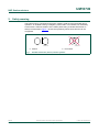
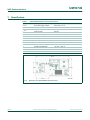
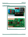
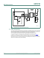
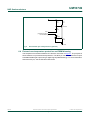
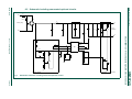
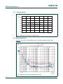
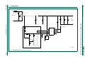
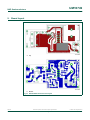
UM10749 SSL5018DB1125 - 230 V/9 W A19 non-isolated buck LED driver demo board Rev. 1 — 6 February 2014 User manual Document information Info Content Keywords SSL5018DB1125, SSL5018TE, LED driver, non-isolated buck typology, A19 applications, HSO8 package Abstract This document describes the performance, technical data and the connection of the SSL5018 demo board, using non-isolated buck topology. The SSL5018 is an NXP Semiconductors driver IC in a HSO8 package, intended to provide a low cost, small form factor LED driver design. This SSL5018DB1125 demo board is designed for T8 applications. It is intended to operate at 230 V (AC), with an output voltage around 35 V. UM10749 NXP Semiconductors SSL5018DB1125 - A19 non-isolated buck LED driver demo board Revision history Rev Date Description v.1 20140206 first issue Contact information For more information, please visit: http://www.nxp.com For sales office addresses, please send an email to: [email protected] UM10749 User manual All information provided in this document is subject to legal disclaimers. Rev. 1 — 6 February 2014 © NXP B.V. 2014. All rights reserved. 2 of 18 UM10749 NXP Semiconductors SSL5018DB1125 - A19 non-isolated buck LED driver demo board 1. Introduction WARNING Lethal voltage and fire ignition hazard The non-insulated high voltages that are present when operating this product, constitute a risk of electric shock, personal injury, death and/or ignition of fire. This product is intended for evaluation purposes only. It shall be operated in a designated test area by personnel qualified according to local requirements and labor laws to work with non-insulated mains voltages and high-voltage circuits. This product shall never be operated unattended. This user manual describes the operation of the SSL5018DB1125 demo board featuring LED driver SSL5018TE in a 230 V/9 W non-isolated application. The SSL5018DB1125 demo board is designed for driving LED loads from 30 V to 40 V with a nominal value of 35 V. The PCB dimensions are compatible with A19 retrofit bulb applications. The demo board provides a simple and effective solution with a high Power Factor (PF), low Total Harmonic Distortion (THD) and high efficiency for Solid State Lighting (SSL) applications. 1.1 Features • • • • • • • • UM10749 User manual A19 retrofit bulb application Open/short LED string protection OverCurrent Protection (OCP) and OverTemperature Protection (OTP) PF > 0.93 and THD < 21 % at nominal 230 V (AC) input Efficiency > 89 % at nominal 230 V (AC) input Compliant with IEC61000-3-2 harmonic standard Compliant with EN55015 conducted EMI PWM dimmable All information provided in this document is subject to legal disclaimers. Rev. 1 — 6 February 2014 © NXP B.V. 2014. All rights reserved. 3 of 18 UM10749 NXP Semiconductors SSL5018DB1125 - A19 non-isolated buck LED driver demo board 2. Safety warning The board must be connected to the mains voltage. Avoid touching the board during operation. An isolated housing is obligatory when used in uncontrolled, non-laboratory environments. Galvanic isolation of the mains phase using a variable transformer is always recommended. Figure 1 shows the symbols by which these devices can be recognized. 019aab174 019aab173 a. Isolated Fig 1. UM10749 User manual b. Not isolated Variable transformer (Variac) isolation symbols All information provided in this document is subject to legal disclaimers. Rev. 1 — 6 February 2014 © NXP B.V. 2014. All rights reserved. 4 of 18 UM10749 NXP Semiconductors SSL5018DB1125 - A19 non-isolated buck LED driver demo board 3. Specification Table 1. Description Value Vmains AC mains supply voltage 230 V (AC) 10 % Pout output power 8.05 W VLED output voltage 30 V to 40 V (35 V nominal value) ILED output current 230 mA Iripple output current ripple 61.7 % (peak-to-peak) ILED/Vmains line regulation 0.4 % at Vmains 10 % ILED/VLED load regulation 0.8 % at VLED 10 % efficiency 89 % at 230 V (AC)/50 Hz PF power factor 0.93 at 230 V (AC)/50 Hz THD total harmonic distortion 21 % at 230 V (AC)/50 Hz Toper operating temperature 40 C to +105 C board dimensions 24 mm 43 mm conducted EMI EN55015 Fig 2. UM10749 User manual SSL5018DB1125 demo board specifications Symbol Dimensions of SSL5018DB1125 demo board All information provided in this document is subject to legal disclaimers. Rev. 1 — 6 February 2014 © NXP B.V. 2014. All rights reserved. 5 of 18 UM10749 NXP Semiconductors SSL5018DB1125 - A19 non-isolated buck LED driver demo board 4. Board photographs a. Top b. Bottom Fig 3. UM10749 User manual SSL5018DB1125 demo board photographs All information provided in this document is subject to legal disclaimers. Rev. 1 — 6 February 2014 © NXP B.V. 2014. All rights reserved. 6 of 18 UM10749 NXP Semiconductors SSL5018DB1125 - A19 non-isolated buck LED driver demo board 5. Connecting the board The board is optimized for a 230 V (AC)/50 Hz mains supply. It is designed to work with multiple LEDs or an LED module. Under the expected conditions, the output current is 230 mA when using an LED string with a 35 V forward voltage (VF). The current can be adjusted using resistors R1 and R2. W1 and W2 are the connections for the mains voltage. J1 (LED+) and J2 (LED-) are the connections for the LED load. Figure 4 shows the connections. Fig 4. Connections of SSL5018DB1125 demo board 6. Functional description 6.1 Input filtering Capacitors C1 and C2 and inductor L1 filter the switching current from the buck converter to the line. Capacitors C1 and C2 also provide a low impedance path for the switching current. The value must to be low to keep the power factor > 0.9. Varistor MOV1 across the AC line provides protection against transient surge voltages. A footprint for an optional Transient Voltage Suppressor (TVS) is available on the board after the Differential-Mode (DM) filter. Diode D4 can be added to increase the immunity to the line surge (see Figure 7). 6.2 Power factor adjustment A power factor improvement circuit is included for high PF and low THD design. Resistors R3, R4, R5, R6, and R7, capacitor C6, and diode D3 modulate the base voltage of transistor Q1 based on the rectified mains. So, transistor Q1 provides modulated current (limited by resistor R8) together with resistor R9 to modulate the peak current detection in the source pin. The peak switching current is modulated based on rectified mains to achieve a high PF and low THD in the design. If the system only allows a power factor of 0.7, the power factor improvement circuit (resistors R3, R4, R5, R6, R7, R8, and R9, capacitor C6, diode D3, and transistor Q1) can be removed. In this case, pins S1 and S2 must be shorted for normal operation. Choose an inductor with a lower Ipeak and decrease the value of output electrolytic capacitor for an even more cost-effective system. UM10749 User manual All information provided in this document is subject to legal disclaimers. Rev. 1 — 6 February 2014 © NXP B.V. 2014. All rights reserved. 7 of 18 UM10749 NXP Semiconductors SSL5018DB1125 - A19 non-isolated buck LED driver demo board 8QPRXQWHG / 8 5 +9 5 6 5 6 5 9&& 5 5 ,& & & '5$,1 *1' '9'7 & 17& 5 5 ' 5 57 4 8QPRXQWHG 5 DDD +LJKSIFLUFXLWU\ Fig 5. SSL5018TE power factor improvement circuit 6.3 Open load protection The driver board is protected when the LED load is accidentally left open. Zener diode D2 sets the threshold voltage. Iit is shorted to trigger the short circuit protection inside the IC when the LED load is open during operation. This open load protection is non-recoverable. Zener diode D2 must be replaced after the protection event. A footprint of optional, recoverable open load protection circuit is shown in Figure 6. Resistor R12 and diode D5 monitor the LED load voltage. Zener diode D5 sets the threshold for turning on transistors Q2 and Q3 and pulling down the NTC pin. It ensures that the IC is switched off to prevent damage. UM10749 User manual All information provided in this document is subject to legal disclaimers. Rev. 1 — 6 February 2014 © NXP B.V. 2014. All rights reserved. 8 of 18 UM10749 NXP Semiconductors SSL5018DB1125 - A19 non-isolated buck LED driver demo board /(' 5 Nȍ 5 Nȍ 4 3%+97 ' =HQHU /(' SXOOGRZQ17&SLQWR WXUQRIIVZLWFKLQJ 4 1 5 Nȍ DDD Fig 6. Recoverable open load protection (optional) 6.4 External overtemperature protection and PWM dimming The footprints of unmounted resistors RT1 and R11 are shown in Figure 7. The purpose of these resistors is to provide thermal protection. The NTC pin can also be used as an input to disable/enable light output using a digital signal (PWM dimming). For more information about the NTC pin, see the SSL5018 data sheet. UM10749 User manual All information provided in this document is subject to legal disclaimers. Rev. 1 — 6 February 2014 © NXP B.V. 2014. All rights reserved. 9 of 18 xxxxxxxxxxxxxxxxxxxxx xxxxxxxxxxxxxxxxxxxxxxxxxx xxxxxxx x x x xxxxxxxxxxxxxxxxxxxxxxxxxxxxxx xxxxxxxxxxxxxxxxxxx xx xx xxxxx xxxxxxxxxxxxxxxxxxxxxxxxxxx xxxxxxxxxxxxxxxxxxx xxxxxx xxxxxxxxxxxxxxxxxxxxxxxxxxxxxxxxxxx xxxxxxxxxxxx x x xxxxxxxxxxxxxxxxxxxxx xxxxxxxxxxxxxxxxxxxxxxxxxxxxxx xxxxx xxxxxxxxxxxxxxxxxxxxxxxxxxxxxxxxxxxxxxxxxxxxxxxxxx xxxxxxxx xxxxxxxxxxxxxxxxxxxxxxxxx xxxxxxxxxxxxxxxxxxxx xxx NXP Semiconductors UM10749 User manual 6.5 Schematic including unmounted optional circuits ) : 029 %' / 9$& - 5 & ' & & 5 5 4 ' : 9 P$ ' - 8QPRXQWHG / 8 5 +9 5 6 5 6 5 9&& 5 5 ,& '5$,1 *1' '9'7 & 17& 5 5 ' & & 5 57 4 4 5 5 Fig 7. SSL5018TE schematic including unmounted optional circuits 8QPRXQWHG DDD UM10749 10 of 18 © NXP B.V. 2014. All rights reserved. +LJKSIFLUFXLWU\ 8QPRXQWHG SSL5018DB1125 - A19 non-isolated buck LED driver demo board Rev. 1 — 6 February 2014 All information provided in this document is subject to legal disclaimers. ' UM10749 NXP Semiconductors SSL5018DB1125 - A19 non-isolated buck LED driver demo board 7. Performance 7.1 Efficiency DDD 9PDLQV9 Fig 8. Efficiency as a function of mains voltage 7.2 Power factor DDD 3) 9PDLQV9 Fig 9. UM10749 User manual Power factor as a function of mains voltage All information provided in this document is subject to legal disclaimers. Rev. 1 — 6 February 2014 © NXP B.V. 2014. All rights reserved. 11 of 18 UM10749 NXP Semiconductors SSL5018DB1125 - A19 non-isolated buck LED driver demo board 7.3 Total harmonic distortion DDD 7+' 9PDLQV9 Fig 10. Total harmonic distortion as a function of mains voltage 7.4 Line regulation ,RXW P$ DDD 9PDLQV9 Fig 11. Output current as a function of mains voltage UM10749 User manual All information provided in this document is subject to legal disclaimers. Rev. 1 — 6 February 2014 © NXP B.V. 2014. All rights reserved. 12 of 18 UM10749 NXP Semiconductors SSL5018DB1125 - A19 non-isolated buck LED driver demo board 7.5 Load regulation ,/(' P$ DDD 9/('9 Fig 12. LED current as a function of LED voltage 7.6 EMI performance Figure 13 shows the conducted EMI result of the SSL5018DB1125 demo board. Fig 13. EMI performance SSL5018DB1125 demo board UM10749 User manual All information provided in this document is subject to legal disclaimers. Rev. 1 — 6 February 2014 © NXP B.V. 2014. All rights reserved. 13 of 18 xxxxxxxxxxxxxxxxxxxxx xxxxxxxxxxxxxxxxxxxxxxxxxx xxxxxxx x x x xxxxxxxxxxxxxxxxxxxxxxxxxxxxxx xxxxxxxxxxxxxxxxxxx xx xx xxxxx xxxxxxxxxxxxxxxxxxxxxxxxxxx xxxxxxxxxxxxxxxxxxx xxxxxx xxxxxxxxxxxxxxxxxxxxxxxxxxxxxxxxxxx xxxxxxxxxxxx x x xxxxxxxxxxxxxxxxxxxxx xxxxxxxxxxxxxxxxxxxxxxxxxxxxxx xxxxx xxxxxxxxxxxxxxxxxxxxxxxxxxxxxxxxxxxxxxxxxxxxxxxxxx xxxxxxxx xxxxxxxxxxxxxxxxxxxxxxxxx xxxxxxxxxxxxxxxxxxxx xxx NXP Semiconductors UM10749 User manual 8. Schematic ) : 0))70 029 029'. %' %6* / 9$& - P+ & ) 9 : & ) 9 & ) 9 5 Nȍ ' 9 =HQHU 9 P$ - / 5/. 8 5 Nȍ +9 5 5 Nȍ 6 Nȍ 6 5 9&& Nȍ 5 Nȍ 5 Nȍ & ) & ) 9 5 ȍ ,& '5$,1 *1' '9'7 17& & S) 9 5 ȍ ' 30// 4 %& 5 Nȍ Fig 14. SSL5018DB1125 demo board schematic DDD UM10749 14 of 18 © NXP B.V. 2014. All rights reserved. +LJKSIFLUFXLWU\ SSL5018DB1125 - A19 non-isolated buck LED driver demo board Rev. 1 — 6 February 2014 All information provided in this document is subject to legal disclaimers. ' (6* UM10749 NXP Semiconductors SSL5018DB1125 - A19 non-isolated buck LED driver demo board 9. Board layout a. Top b. Bottom Fig 15. SSL5018DB1125 demo board layout UM10749 User manual All information provided in this document is subject to legal disclaimers. Rev. 1 — 6 February 2014 © NXP B.V. 2014. All rights reserved. 15 of 18 UM10749 NXP Semiconductors SSL5018DB1125 - A19 non-isolated buck LED driver demo board 10. Bill Of Materials (BOM) Table 2. SSL5018DB1125 demo board BOM Reference Description and values Part number Manufacturer C1; C2 capacitor; 0.1 F; 450 V ECW-F2W104JAQ Panasonic C3 capacitor; 330 F; 50 V EEU-EB1H331 Panasonic C4 capacitor; 120 pF; 450 V; C0G; 0805 CGA4C4C0G2W121J060AA TDK C5 capacitor; 4.7 F; 25 V; X7R; 1206 C3216X7R1E475K160AC TDK C6 capacitor; 0.47 F; 50 V; X7R; 0603 UMK107B7474KA-TR Taiyo Yuden BD1 bridge rectifier; 600 V; 0.8 A B6S-G Comchip Tech D1 fast diode; 400 V; 1 A ES1G Fairchild Semiconductor D2 zener diode; 47 V4 SMAJ5941B-TP Micro Commercial D3 diode; 75 V; 200 mA PMLL4148 NXP Semiconductors L1 inductor; 3300 H RLB0812-332KL Bourns L2 inductor; 820 H RL-7500-4-821K Renco Electronics Q1 transistor; 45 V; PNP BC857 NXP Semiconductors R1 resistor; 0.62 ; 0805 RCWE0805R620FKEA Vishay Dale R2 resistor; 25.5 ; 0805 ERJ-6ENF25R5V Panasonic R3; R4 resistor; 681 k; 1206 ERJ-8ENF6813V Panasonic R5 resistor; 33 k; 0603 ERJ-3EKF3302V Panasonic R6 resistor; 68.1 k; 0603 ERJ-3EKF6812V Panasonic R7 resistor; 562 k; 0603 ERJ-3EKF5623V Panasonic R8 resistor; 33 k; 0603 ERJ-3EKF3302V Panasonic R9 resistor; 4.75 k; 0603 ERJ-3EKF4751V Panasonic R10 resistor; 80.6 k; 0805 ERJ-3EKF8062V Panasonic MOV1 varistor; 250 V (AC) MOV-10D431K Bourns U1 IC; SSL5018; HSO8 SSL5018TE NXP Semiconductors F1 fuse; 250 V (AC); 1 A; 2410 MF2410F1.000TM AME UM10749 User manual All information provided in this document is subject to legal disclaimers. Rev. 1 — 6 February 2014 © NXP B.V. 2014. All rights reserved. 16 of 18 UM10749 NXP Semiconductors SSL5018DB1125 - A19 non-isolated buck LED driver demo board 11. Legal information 11.1 Definitions Draft — The document is a draft version only. The content is still under internal review and subject to formal approval, which may result in modifications or additions. NXP Semiconductors does not give any representations or warranties as to the accuracy or completeness of information included herein and shall have no liability for the consequences of use of such information. 11.2 NXP Semiconductors does not accept any liability related to any default, damage, costs or problem which is based on any weakness or default in the customer’s applications or products, or the application or use by customer’s third party customer(s). Customer is responsible for doing all necessary testing for the customer’s applications and products using NXP Semiconductors products in order to avoid a default of the applications and the products or of the application or use by customer’s third party customer(s). NXP does not accept any liability in this respect. Export control — This document as well as the item(s) described herein may be subject to export control regulations. Export might require a prior authorization from competent authorities. Disclaimers Limited warranty and liability — Information in this document is believed to be accurate and reliable. However, NXP Semiconductors does not give any representations or warranties, expressed or implied, as to the accuracy or completeness of such information and shall have no liability for the consequences of use of such information. NXP Semiconductors takes no responsibility for the content in this document if provided by an information source outside of NXP Semiconductors. In no event shall NXP Semiconductors be liable for any indirect, incidental, punitive, special or consequential damages (including - without limitation - lost profits, lost savings, business interruption, costs related to the removal or replacement of any products or rework charges) whether or not such damages are based on tort (including negligence), warranty, breach of contract or any other legal theory. Notwithstanding any damages that customer might incur for any reason whatsoever, NXP Semiconductors’ aggregate and cumulative liability towards customer for the products described herein shall be limited in accordance with the Terms and conditions of commercial sale of NXP Semiconductors. Right to make changes — NXP Semiconductors reserves the right to make changes to information published in this document, including without limitation specifications and product descriptions, at any time and without notice. This document supersedes and replaces all information supplied prior to the publication hereof. Suitability for use — NXP Semiconductors products are not designed, authorized or warranted to be suitable for use in life support, life-critical or safety-critical systems or equipment, nor in applications where failure or malfunction of an NXP Semiconductors product can reasonably be expected to result in personal injury, death or severe property or environmental damage. NXP Semiconductors and its suppliers accept no liability for inclusion and/or use of NXP Semiconductors products in such equipment or applications and therefore such inclusion and/or use is at the customer’s own risk. Applications — Applications that are described herein for any of these products are for illustrative purposes only. NXP Semiconductors makes no representation or warranty that such applications will be suitable for the specified use without further testing or modification. Customers are responsible for the design and operation of their applications and products using NXP Semiconductors products, and NXP Semiconductors accepts no liability for any assistance with applications or customer product design. It is customer’s sole responsibility to determine whether the NXP Semiconductors product is suitable and fit for the customer’s applications and products planned, as well as for the planned application and use of customer’s third party customer(s). Customers should provide appropriate design and operating safeguards to minimize the risks associated with their applications and products. Evaluation products — This product is provided on an “as is” and “with all faults” basis for evaluation purposes only. NXP Semiconductors, its affiliates and their suppliers expressly disclaim all warranties, whether express, implied or statutory, including but not limited to the implied warranties of non-infringement, merchantability and fitness for a particular purpose. The entire risk as to the quality, or arising out of the use or performance, of this product remains with customer. In no event shall NXP Semiconductors, its affiliates or their suppliers be liable to customer for any special, indirect, consequential, punitive or incidental damages (including without limitation damages for loss of business, business interruption, loss of use, loss of data or information, and the like) arising out the use of or inability to use the product, whether or not based on tort (including negligence), strict liability, breach of contract, breach of warranty or any other theory, even if advised of the possibility of such damages. Notwithstanding any damages that customer might incur for any reason whatsoever (including without limitation, all damages referenced above and all direct or general damages), the entire liability of NXP Semiconductors, its affiliates and their suppliers and customer’s exclusive remedy for all of the foregoing shall be limited to actual damages incurred by customer based on reasonable reliance up to the greater of the amount actually paid by customer for the product or five dollars (US$5.00). The foregoing limitations, exclusions and disclaimers shall apply to the maximum extent permitted by applicable law, even if any remedy fails of its essential purpose. Safety of high-voltage evaluation products — The non-insulated high voltages that are present when operating this product, constitute a risk of electric shock, personal injury, death and/or ignition of fire. This product is intended for evaluation purposes only. It shall be operated in a designated test area by personnel that is qualified according to local requirements and labor laws to work with non-insulated mains voltages and high-voltage circuits. The product does not comply with IEC 60950 based national or regional safety standards. NXP Semiconductors does not accept any liability for damages incurred due to inappropriate use of this product or related to non-insulated high voltages. Any use of this product is at customer’s own risk and liability. The customer shall fully indemnify and hold harmless NXP Semiconductors from any liability, damages and claims resulting from the use of the product. Translations — A non-English (translated) version of a document is for reference only. The English version shall prevail in case of any discrepancy between the translated and English versions. 11.3 Trademarks Notice: All referenced brands, product names, service names and trademarks are the property of their respective owners. GreenChip — is a trademark of NXP B.V. UM10749 User manual All information provided in this document is subject to legal disclaimers. Rev. 1 — 6 February 2014 © NXP B.V. 2014. All rights reserved. 17 of 18 UM10749 NXP Semiconductors SSL5018DB1125 - A19 non-isolated buck LED driver demo board 12. Contents 1 1.1 2 3 4 5 6 6.1 6.2 6.3 6.4 6.5 7 7.1 7.2 7.3 7.4 7.5 7.6 8 9 10 11 11.1 11.2 11.3 12 Introduction . . . . . . . . . . . . . . . . . . . . . . . . . . . . 3 Features . . . . . . . . . . . . . . . . . . . . . . . . . . . . . . 3 Safety warning . . . . . . . . . . . . . . . . . . . . . . . . . . 4 Specification. . . . . . . . . . . . . . . . . . . . . . . . . . . . 5 Board photographs . . . . . . . . . . . . . . . . . . . . . . 6 Connecting the board . . . . . . . . . . . . . . . . . . . . 7 Functional description . . . . . . . . . . . . . . . . . . . 7 Input filtering . . . . . . . . . . . . . . . . . . . . . . . . . . . 7 Power factor adjustment . . . . . . . . . . . . . . . . . . 7 Open load protection . . . . . . . . . . . . . . . . . . . . 8 External overtemperature protection and PWM dimming . . . . . . . . . . . . . . . . . . . . . . 9 Schematic including unmounted optional circuits . . . . . . . . . . . . . . . . . . . . . . . . 10 Performance . . . . . . . . . . . . . . . . . . . . . . . . . . . 11 Efficiency . . . . . . . . . . . . . . . . . . . . . . . . . . . . 11 Power factor . . . . . . . . . . . . . . . . . . . . . . . . . . 11 Total harmonic distortion. . . . . . . . . . . . . . . . . 12 Line regulation . . . . . . . . . . . . . . . . . . . . . . . . 12 Load regulation . . . . . . . . . . . . . . . . . . . . . . . . 13 EMI performance . . . . . . . . . . . . . . . . . . . . . . 13 Schematic . . . . . . . . . . . . . . . . . . . . . . . . . . . . . 14 Board layout . . . . . . . . . . . . . . . . . . . . . . . . . . . 15 Bill Of Materials (BOM) . . . . . . . . . . . . . . . . . . 16 Legal information. . . . . . . . . . . . . . . . . . . . . . . 17 Definitions . . . . . . . . . . . . . . . . . . . . . . . . . . . . 17 Disclaimers . . . . . . . . . . . . . . . . . . . . . . . . . . . 17 Trademarks. . . . . . . . . . . . . . . . . . . . . . . . . . . 17 Contents . . . . . . . . . . . . . . . . . . . . . . . . . . . . . . 18 Please be aware that important notices concerning this document and the product(s) described herein, have been included in section ‘Legal information’. © NXP B.V. 2014. All rights reserved. For more information, please visit: http://www.nxp.com For sales office addresses, please send an email to: [email protected] Date of release: 6 February 2014 Document identifier: UM10749