1
D
D
D
D
D
R
R
R
R
R
D
R
R
R
A
FT
R
A
F
FT
FT
A
A
R
R
D
D
D
D
FT
FT
A
A
R
R
D
Input parameters:
D
R
FT
FT
A
A
R
R
D
D
D
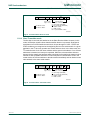
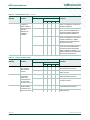
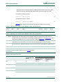
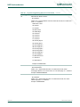
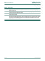
Read Sector CRC
FT
FT
FT
FT
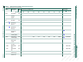
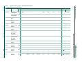
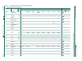
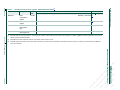
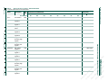
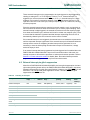
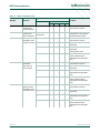
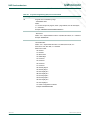
IAP call parameters
A
A
A
A
R
R
D
D
D
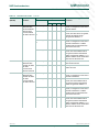
IAP function calls …continued
IAP function
FT
FT
FT
FT
FT
UM<nnnnn>
P89LPC9201/9211/922A1/9241/9251 User manual
Table 97.
A
A
A
A
A
NXP Semiconductors
D
D
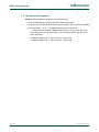
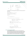
ACC = 05h
R
A
R7= sector address
FT
D
Return parameter(s):
R
A
R4= CRC bits 31:24
R5= CRC bits 23:16
R6= CRC bits 15:8
R7= CRC bits 7:0 (if no error)
R7= error status (if error)
Carry= set on error, clear on no error
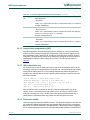
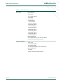
Read Global CRC
Input parameters:
ACC = 06h
Return parameter(s):
R4= CRC bits 31:24
R5= CRC bits 23:16
R6= CRC bits 15:8
R7= CRC bits 7:0 (if no error)
R7= error status (if error)
Carry= set on error, clear on no error
Read User Code
Input parameters:
ACC = 07h
R4= address (MSB)
R5= address (LSB)
Return parameter(s):
R7= data
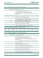
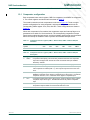
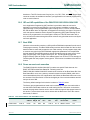
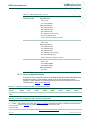
16.17 User configuration bytes
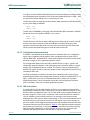
A number of user-configurable features of the P89LPC9201/9211/922A1/9241/9251 must
be defined at power-up and therefore cannot be set by the program after start of
execution. These features are configured through the use of an Flash byte UCFG1 and
UCFG2 shown in Table 99 and Table 102.
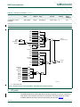
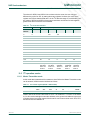
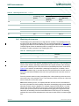
Table 98.
Flash User Configuration Byte 1 (UCFG1) bit allocation
Bit
7
6
5
4
3
2
1
0
Symbol
WDTE
RPE
BOE1
WDSE
BOE0
FOSC2
FOSC1
FOSC0
Unprogrammed
value
0
1
1
0
0
0
1
1
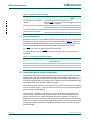
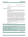
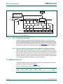
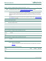
Table 99.
Flash User Configuration Byte 1 (UCFG1) bit description
Bit Symbol
Description
0
FOSC0
1
FOSC1
CPU oscillator type select. See Section 2 “Clocks” for additional information. Combinations other than those
shown in Table 100 are reserved for future use and should not be used.
2
FOSC2
3
BOE0
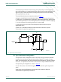
Brownout Detect Configuration (see Section 6.1 “Brownout detection”)
<Document ID>
User manual
© NXP B.V. 2009. All rights reserved.
Rev. 01.xx — 5 February 2009
114 of 136