1
DS92LV16
Literature Number: SNLA201
National Semiconductor
DS92LV16 Design Guide
October 2002
• Bus LVDS SerDes
Architecture
— page 3
• Bus Topologies
— page 4
• Backplanes
— page 5
• PCB Recommendations
— page 6
• Cables & Connectors
— page 7
• Power & Ground
— pages 8-9
• Clocking
— page 10
• Inputs & Outputs
— page 11
• Evaluating the DS92LV16
— page 12
• Loopback Testing
— page 13
• Lock to Random Data vs.
Sync Patterns
— page 14
• Interconnect Jitter Budget
— pages 15-17
• Troubleshooting
— page 18
• Additional Resources
—page 19
Serializing Made Simple
www.national.com/lvds
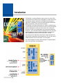
Introduction
The DS92LV16 is a member of National’s robust and easy-to-use Bus LVDS
serializer/deserializer (SerDes) family already popular in a wide variety of telecom, datacom, industrial, and commercial backplane/cable interconnect
applications. The DS92LV16 is similar to the original 10-bit Bus LVDS SerDes
products, but provides a wider, 16-bit data bus payload.
The DS92LV16 is very flexible and performs over a wide, 25 - 80 MHz frequency range. Both the transmit clock and receiver reference clock have high jitter
tolerance, allowing the use of low cost clock sources. The serializer and
deserializer sections are fully independent and can be operated at different
frequencies. This is useful when upstream and downstream rates are not balanced. In addition, the serializer and deserializer blocks can be powered
down independently if only one transmission direction is needed.
The receiver locks to random data, eliminating the need to interrupt normal
traffic with PLL training patterns after hot plug events. The usual loss-of-lock
feedback path from receiver to transmitter is also not required.
Line and local loopback test modes allow the designer to segregate portions
of the system to facilitate system diagnostics.
2
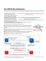
Bus LVDS SerDes Architecture
The Bus LVDS SerDes architecture was
developed in conjunction with major
telecommunications customers who desired
features not provided by common 8b/10b
datacom SerDes chipsets. Instead of scrambling each byte into a new 10-bit code as
with 8b/10b coding, the Bus LVDS SerDes
coding scheme frames each data word with
DS92LV16 embedded clock coding scheme showing 16 data bits plus clock 0,1 bits.
two embedded clock bits, one high and one
low. These embedded clock bits create a rising edge transition which provides precise timing
and framing information to the receiver on every clock cycle.
The resulting benefits of the Bus LVDS SerDes architecture include:
■ Lock to random data for true hot plug capability—lock can be achieved without interrupting
traffic with PLL training patterns and without a loss-of-lock feedback path from receiver to
transmitter.
■ The relaxed ±5% RefCLK frequency specification means the receiver does not require a precise reference clock source to recover data reliably.
■ Jitter-tolerant TCLK transmit clock input eliminates the requirement to use a high-grade telecom/datacom transmit clock source and also simplifies external loopback operations.
■ Non-byte-oriented bus widths such as 10-bits are available.
Overview comparing the DS92LV16 to 8b/10b SerDes architectures.
3
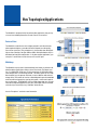
Bus Topologies/Applications
The DS92LV16 is designed mainly for point-to-point applications, but you may
also use it for multidrop interconnects under certain circumstances.
Point-to-Point
The DS92LV16 can deliver the full 1.28 Gbps payload in each direction over
point-to-point backplanes and cables (distance depends on cable quality,
transmission speed, etc.) This performance is also possible when driving multiple receivers through a low jitter LVDS-to-LVDS switch/distribution chip in a
distributed point-to-point configuration. In all point-to-point applications, you
must place a termination resistor close to each receiver input.
Multidrop
The DS92LV16 may be used in limited multidrop (also known as point-to-multipoint) backplane applications driving a few receiver loads. The output structure is a modified Bus LVDS-type circuit that regulates the VOD (output differential voltage) over a narrow range of loads. The driver expects to see a 100Ohm load, but may also operate with loads as low as 50 Ohms with reduced
voltage swing. The number of receivers allowed depends upon the bandwidth
of the interconnecting path, the spacing of the nodes, and also the length of
the resulting stubs. The DS92LV16’s fast Bus LVDS output edge rates are optimized for the high throughput of the part, thus stub length must be minimized
mechanically or electrically using “stub hider” buffer devices.
See the “Backplane” section for more information.
4
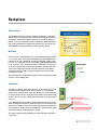
Backplanes
Point-to-Point
The DS92LV16 achieves the maximum 1.28 Gbps performance in controlled
100-Ohm differential impedance point-to-point or distributed point-to-point FR4 backplanes, though other backplane materials such as GETEK, Rogers, or
hybrids may also be employed if desired. The backplane should be designed
with sufficient bandwidth to support the desired data rate. For example, for 1
Gbps (500 MHz), a media bandwidth of 1.5 GHz is typically required.
Multidrop
In some instances, the DS92LV16 may be used in multidrop backplanes driving
a 2 - 4 receiver loads. Actual performance depends on the bandwidth of the
interconnect. Pay close attention on minimizing stub lengths (connector plus
trace) to < 2 cm. Depending on data rate, National’s LVDS DS90LV001 or other
future “stub hider” chips should used to reduce stub lengths seen by the signal on the backplane. Receiver loads should be widely spaced to reduce the
transmission segment to stub length ratio and/or placed far away from the
transmitter to allow the edge rate to be slowed by the interconnect before
reaching the first stub.
Due to fast edge rates, the DS92LV16 is typically not recommended for driving
more than a few multidrop loads.
Termination
Termination is required. Choose the termination resistor value RL to match the
loaded differential impedance of the transmission line. In a point-to-point
backplane, the termination value is typically 100 Ohms. If a smaller output signal swing is desired, the line may be terminated at both the transmitter output
as well as the receiver input, reducing the effective load seen by the transmitter by half.
In a multidrop backplane, the added capacitive loading of the extra receivers
lowers the differential impedance, requiring a lower value termination resistor.
Again, the termination resistor(s) value chosen should match the loaded backplane impedance. Note that loads less than 50 Ohms reduce the output signal
swing below ±350 mV, compromising noise margins.
The typical capacitance of the DS92LV16 serial Bus LVDS inputs and outputs
is about 5 pF.
5
PCB Recommendations
General Printed Circuit Board (PCB) Recommendations
■ Use at least 4 PCB board layers (Bus LVDS signals, ground, power, and TTL
signals).
■ Minimize any resulting stub lengths—
In a point-to-point bus, the resulting stub is typically the distance between the
termination resistor and the receiver input pins of the DS92LV16. Place the
small surface mount resistor as close to the receiver input pins as possible.
In a limited multidrop bus, the termination is typically at the far end of the bus
only. The resulting stubs are from the main line to the receiver inputs and
these distances should be minimized.
Minimize “s” and adjust “W’” for proper differential impedance.
■ Segment impedance matching – in a backplane point-to-point bus, the
location of the serializer and deserializer is less critical. More important is
matching the impedance of all transmission line segments. These impedances should be matched within 10% of the nominal value.
■ Controlled impedance differential traces of 100 Ohms are typically recommended for Bus LVDS signals. Edge-coupled microstrip, edge-coupled
stripline, or broadside-coupled stripline differential traces may be used. These
traces should be closely-coupled (i.e. “s” should be minimized) to ensure coupled noise will appear as common-mode (which is rejected by the receiver).
This has the added benefit that closely-coupled lines that are excited with
odd-mode transmission tend to radiate less electromagnetic energy.
■ Treat the LVDS pair as one signal, avoiding influences that cause imbalances within the pair (see diagram at left). Minimize skew within the pair.
Maintain “balance.”
The LVDS pair should be treated as “one signal.”
Avoid unbalancing influences and keep TTL lines
away from the LVDS pair.
! Tip
Designing with LVDS is actually quite easy if you
remember that LVDS is a high speed, differential
signaling technology.
High Speed: LVDS pairs should be considered
transmission lines. Anything over a few centimeters should have controlled impedance. LVDS termination is always required.
Differential: Each LVDS pair should be treated as
one signal. Both wires of ech pair should “see”
the same electrical path.
6
■ Leave unused Bus LVDS receiver inputs open (floating) – the internal failsafe in the DS92LV16 will pull the input to a valid state.
■ Termination of the Bus LVDS signals is required. The termination resistor
value should match the differential impedance of the transmission line. 100Ohm is a typical value for point-to-point applications. It is better err with too
large a termination resistor than too small.
■ Isolate TTL/CMOS signals from Bus LVDS signals, placing them at least
“3s” or “2w” away—whichever is larger. This will help to prevent them from
coupling onto the LVDS lines.
These are just a few common practices that should be followed when designing PCBs for LVDS signaling. General application guidelines are available in
the LVDS Owner's Manual and other documents at www.national.com/lvds.
Cables & Connectors
Cables
The DS92LV16 can be used over a wide variety of balanced cables depending
on distance and signal quality requirements. In general, twinax or twisted pair
cables are recommended.
■ Typical Connections can be made using category 5 (CAT5) twisted pair ethernet cable with RJ-45 connectors. See graph at right for typical data rate versus cable distance.
■ Higher Speed Links: AMP Z-PACK® cables or other twinax cables can be
used.
■ Higher Pincount: SCSI-type cables and connectors or LVDS-type cable
assemblies such as the 3M™ MDR and Amphenol SKEWCLEAR® systems are
commonly used.
■ Very Short Distances (< 0.3 m): flex circuit (following correct PCB layout) or
unbalanced ribbon cable may even be used.
Typical CAT5 ethernet cable length versus frequency.
If running multiple Bus LVDS pairs in the same cable assembly, use individually shielded pairs to minimize crosstalk between the pairs. At least one ground
conductor should be used in the cable (connecting to the DS92LV16 analog
grounds (AGNDs)) to provide a known, low impedance return path for common mode currents.
A termination resistor RL, placed as close as possible to the receiver inputs in
point-to-point applications, is required. The resistor value should be chosen to
match the differential impedance of the cable.
Connectors
CAT5 ethernet cable with RJ-45 connectors.
Connectors with differential conductors offer the highest performance, but are
not necessary in typical, lower speed or short distance applications. For single-ended connectors, keep LVDS pins away from other signals, particularly
TTL/CMOS/LVTTL/LVCMOS signals. The “+” and “-” signals of a pair should be
routed on the same row in multi-row connectors to help minimize skew. For
high-speed applications (> 800 Mbps) using differential-optimized connectors
is recommended.
Twinax-type cable assembly.
7
Power & Ground
General Recommendations
A solid power/ground system is the foundation on which a reliable interconnect system is built. Design circuit board layout and stackup for the system to provide noise-free power to the device. Good layout practice will separate high frequency and high level inputs and
outputs to minimize unwanted stray noise pickup, feedback, and interference. Power system performance may be greatly improved by
using thin dielectrics (4 to 10 mils) for power/ground sandwiches. This increases the intrinsic capacitance of the PCB power system,
which improves power supply filtering—especially at high frequencies—making the value and placement of external bypass capacitors less critical. External bypass capacitors should include both RF ceramic and tantalum electrolytic types. Use RF capacitors in the
range of 0.001 µF to 0.1 µF. Use tantalum capacitors in the range of 2.2 µF to 10 µF. The voltage rating of tantalum capacitors should be
at least 3 (5 preferred) times the power supply voltage being used.
It is recommended practice to use two vias at each power/ground pin as well as all RF bypass capacitor terminals. Dual vias reduce
the interconnect inductance by up to half, thereby extending the effective range of bypass components. Locate RF capacitors as close
as possible to the supply pins and use wide, low impedance traces—not 50-Ohm traces. Surface mount capacitors are recommended
due to lower parasitics. When using multiple capacitors per supply pin, locate the smallest value closest to the supply pin. A bulk capacitor is recommended at the point of power entry. This is typically in the range of 50 µF to 100 µF and will smooth low frequency noise.
Some devices have separate power/ground pins for different portions of the circuits to isolate switching noise effects between different blocks. Connecting these to separate power/ground planes on the PCB is typically not required. Pin description tables typically
describe which blocks are connected to which power/ground pins. In some cases, an external filter may be used to provide clean power
to sensitive circuits such as PLLs.
DS92LV16 Recommendations
General device-specific bypassing recommendations are given below. Actual best practice depends on other board and system level
criteria including board density, power rail and power supply type, and the supply needs of other integrated circuits on the board.
PVDD/PGND PLL Supply
The PVDD pins (the DS92LV16 has 2 PVDD pins) supply the PLL circuits. PLLs require a clean supply—less than 100 mV noise peak-topeak—for the minimization of jitter. PVDD noise in the frequency range 200 kHZ to 5 MHz can increase jitter and reduce noise margins.
Certain power supplies may have switching frequencies or high harmonic content in this range. If this is the case, filtering of this noise
spectrum may be required. A notch filter response is best to provide stable VDD, suppression of the noise band, and good high frequency response (clock fundamental). This may be accomplished with a CRC or CLC pie filter. If employed, a separate pie filter is recommended for each PLL to minimize the voltage drop due to series resistance. Separate board power planes for each PVDD are typically not required.
AVDD/AGND LVDS Supply
The AVDD pins (the DS92LV16 has 4 AVDD pins) supply the LVDS ciruits. Due to the nature of the DS92LV16 design, large currents are
not drawn through these pins and a 0.1 µF capacitor is sufficient for these pins. If space is available, a 0.01 µF capacitor may be used
in parallel with the 0.1 µF capacitor for additional high frequency filtering. Connect the AGND ground to the cable ground to provide a
8
Power & Ground (continued)
return path for any common (even) mode currents. Most of the LVDS current is
odd-mode and returns within the pair, though a small amount of odd-mode current may be present due to coupled noise and the cable ground should return
through a low impedance path to AGND.
DVDD/DGND Digital Supply
The DVDD pins supply the digital portion of the device and also the receiver output drivers. The receiver DVDD is more critical than the transmitter DVDD
because it must power the receiver outputs during multiple output switching
conditions. Four DS92LV16 receiver outputs are powered by each DVDD pin,
suggesting that a minimum local bypass capacitance of 28 nF is required. This
is calculated by taking 4 times the maximum short circuit current (4 x 85 mA =
340 mA), multiplying by the output rise time (4 ns), and then dividing by the maximum allowed VDD droop (assume 50 mV) and yields 27.2 nF. Rounding up, a
standard 0.1 µF is selected for each DVDD pin.
Power Up Sequencing
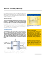
DS92LV16 typical total IDD versus frequency. (3.3
V, 25° C)
! Tip
Comparing Power Consumption
The DS92LV16 does not require a specific power up sequence. Best practice is:
power up all VDD pins together, apply clocks (RefCLK & TCLK), and then bring
/PWDN powerdown pins high to enable the transmit and/or receive channels.
The chip has a power-on reset (POR) circuitry which holds the outputs in TRISTATE until the supply is above approximately 2.5V. Since all VDD pins (PVDD,
AVDD, & DVDD) are related internally, they must be powered up and down
together.
There is no industry-standard method for specifying power consumption in SerDes datasheets.
Power consumption varies significantly with output load, pattern, clock frequency, and the number
of channels tested. Even so-called “worst-case”
power consumption conditions vary greatly from
vendor to vendor. For instance, many vendors do
not include the receiver parallel output bus load
current.
The DS92LV16 maximum datasheet power consumption is specified at worst case voltage (3.6 V),
temperature, and pattern (checkerboard, i.e. alternating LVTTL ones and zeros) with 15 pF load on
all CMOS outputs and both transmit & receive
channels running at maximum clock frequency (80
MHz).
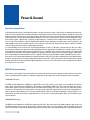
Typical connection diagram showing power supply bypassing. Employ sufficient bypassing to ensure < 100 mV peak-to-peak noise on supply pins, especially PVDD. Each DVDD pin should have separate bypass capacitance.
9
Clocking
Transmit Clock (TCLK)
The transmit clock (TCLK) rising edge is used by the transmit block to latch in
the DIN[0:15] parallel bus and run the transmitter’s PLL. The TCLK input is
LVTTL/LVCMOS compatible.
The TCLK clock input tolerates jitter of 80 ps RMS allowing the use of nontelecom/datacom-grade clock sources. The receiver output clock RCLK can
also be fed back to TCLK and data retransmitted as an external loopback or
repeater, though only two “hops” total are recommended before filtering out
accumulated clock jitter. Excessive jitter, especially in the range of 200 kHz - 2
MHz, can appear on the serial outputs reducing link noise margins.
Be careful not to confuse RMS and peak-to-peak jitter. For a typical clock signal with mostly random jitter (i.e. gaussian distribution), the jitter tolerance of
80 ps RMS is by definition approximately 1128 ps peak-to-peak at a 10-12 bit
error rate (BER).
If TCLK is interrupted, the chipset will go through the resynchronization procedure upon reapplication of valid TCLK.
Receiver Reference Clock (RefCLK)
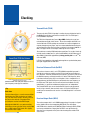
Maximum RMS TCLK input jitter tolerance versus
jitter frequency under typical conditions.
The receiver reference clock is an LVTTL/LVCMOS compatible input and is
used by the receiver to establish receiver PLL lock and prevent locking to a
false harmonic. Therefore, the RefCLK characteristics are not very critical and
the RefCLK frequency need only be within ±5% of the TCLK frequency of the
transmitter from which the chip is receiving data. Unless a loopback test is
being performed, this RefCLK frequency need not be the same frequency as
the chip’s own TCLK signal since the transmit and receive blocks are fully
independent, i.e. upstream and downstream data rates are independent..
The relaxed RefCLK specs mean that the RefCLK signal can be generated
locally using a common, low cost clock source. In fact, the RefCLK signal
could even be removed once the receiver is locked (though this is not recommended).
! Tip
Clock Jitter
The transmitter will pass a certain amount of jitter
contained on the TCLK clock to the serial data.
This can affect noise margins. Similarly, some of
the jitter on the clock 0,1 rising edge will be
passed by the receiver to the RCLK output.
Although the DS92LV16 is very tolerant to jitter,
minimizing cycle-to-cycle jitter in the range of 200
kHz - 2 MHz on both TCLK and the PLL supplies
will maximize noise margins.
10
Receiver Output Clock (RCLK)
The receiver output clock is an LVCMOS output whose rising edge is aligned
to the middle of the receiver output data ROUT[0:15]. The subsequent
ASIC/FPGA device should latch in ROUT[0:15] data meeting the ASIC’s/FPGA’s
input setup and hold times. Output jitter for RCLK is not specified on the
datasheet since it depends on the jitter of the incoming data and the TCLK
clock source.
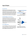
Inputs & Outputs
Unused LVTTL Inputs
Unused LVTTL inputs may be left floating or tied high or low. The device
datasheet indicates the presence of pull down devices to bias unused pins.
These internal impedances tend to be in the 200 kOhm range and may be
overridden with lower value pull up resistors if desired. If not using the full 16
bits of the payload, careful attention needs to be taken to avoid disrupting the
random lock feature. These unused bits will still be transmitted, so in order for
the receiver to maintain random data lock capability, care must be taken not
to create a situation where the unused bits cause a repetitive multiple lowhigh transitions (RMTs). Avoid this by tying bits high at the LSB inputs (starting
with DIN0) and bits tied low at the MSB inputs (inputs ending with DIN16).
Example showing two unused bits pulled high and
two unused bits pulled low to avoid RMTs.
Floating Bus LVDS Receiver Inputs & Failsafe
In the event that the DS92LV16 receiver is disconnected from the
backplane/cable, the internal failsafe circuitry is designed to reject a certain
amount of differential noise (about 10mV) from being interpreted as data or
clock. This seems like a very small threshold, but balanced, closely-coupled
LVDS lines tend to pick up noise as common mode—not differential. The
CMOS ROUT[0:15] outputs of the DS92LV16 deserializer will be TRI-STATE
when the incoming serial data is removed and the receiver loses lock.
Additional failsafe biasing can be implemented externally (see application
note AN-1194 and LVDS Owner’s Manual sections 4.6.2-3) at the expense of
two additional resistors.
Receiver CMOS Output Drive
The receiver CMOS outputs are specified at ±9 mA. This is typically sufficient
to drive 2-3 LVTTL/LVCMOS loads. If more loads will be driven, especially at
higher clock speeds, a logic buffer is recommended. Note that depending on
actual configuration (number of loads, stub lengths, segment distances, etc.),
the receiver output bus may need to be treated as a transmission line and
proper LVTTL/LVCMOS termination techniques employed.
An example of external faisafe biasing for the
DS92LV16. See application note AN-1194 and
LVDS Owner’s Manual sections 4.6.2-3 for details.
11
Evaluating the DS92LV16
Evaluation Board
The DS92LV16 evaluation kit provides the ability to evaluate the DS92LV16 over
AMP Z-Pack cables (1 meter cable included) or any user-supplied interconnect (modified to connect to the boards). The user manual can be downloaded
from the web at www.national.com/lvds and the kit itself ordered from authorized distributors as part number BLVDS16EVK subject to availability.
Probing Bus LVDS Signals
DS92LV16 eval kit (order number BLVDS16EVK).
LVDS signals are high speed, low swing signals. Improper probing can result
in deceiving results since the probe and/or scope can filter high speed coponents of the signal. Using a ≥1 GHz bandwidth scope (such as the Agilent
86100 or Tektronix 694C) and a high speed differential probe (such as the
Tektronix P6247/8 or P6330) is highly recommended. LVDS drivers are not compatible with 50-Ohm probes.
PRBS pattern at serializer output . Note the embedded
low/high clock 0/1 bits.
Tektronix 1GHz P6247 differential probe. Note two
probe contacts and polarity indication in probe tip
detail.
12
SYNC pattern at serializer output.
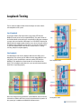
Loopback Testing
The line and local loopback modes allow the designer to isolate and test
selected portions of the system.
Local Loopback
Asserting the LOCAL_LE pin high connects the parallel LVTTL data bus
DIN[0:15] internally to the receiver output ROUT[0:15]. This mode includes all
the functional blocks of the SerDes pair except the Bus LVDS input and output
structures (the transmitter Bus LVDS outputs are in TRI-STATE). Switching the
DS92LV16 to local loopback mode, therefore, means the receiver will relock to
the loopback data and RefCLK must be within ±5 % of the local TCLK frequency. The local loopback mode allows the local card to verify it is sending,
receiving, and processing data properly.
Line Loopback
The DS92LV16 will enter the line loopback mode when the LINE_LE pin is
brought high. This connects the Bus LVDS transmitter output (DO) pins internally to the receiver input (RIN) pins and to the parallel LVTTL data bus
ROUT[0:15]. This loopback test mode includes the serializer/deserializer
blocks. The line loopback mode allows the system to verify that the board-toboard links are operating properly.
Due to the relaxed clocking requirements of the DS92LV16, external line loopback within an FPGA or ASIC can also easily be performed to test portions of
the system logic in addition to the DS92LV16 and interconnect.
Local loopback mode.
Line loopback mode.
13
Lock to Random Data vs. SYNC Patterns
SYNC Patterns
SYNC patterns, “H1111111100000000L” where “H” is the clock 1 bit (high) and
“L” is the clock 0 bit (low), are sent automatically by the transmitter when the
SYNC pin is held high. The receiver will lock to this pattern within a guaranteed time (see tDSR specified in the datasheet). When the deserializer’s /LOCK
pin goes high, the receiver has locked to the incoming data stream and valid
data appears at the receiver outputs.
Lock to Random Data
The receiver will also lock to random data without external system intervention, providing a powerful “plug & go” system capability not provided by most
SerDes chipsets. In order to achieve this, the receiver looks for a consistent
low-high transition caused by the clock 0,1 bits. If there are two data bits consistently “stuck” low-high over multiple clock cycles (known as a repetitive
multiple transition or RMT), the receiver will not lock until these bits change
and the receiver recognizes the unique embedded clock low-to-high transition.
Incoming data stream (arranged in 18-bit words)
showing no RMT’s. Receiver will aqcuire lock.
Sending SYNC Patterns versus Lock to Random Data
Sending SYNC patterns has the advantage that the receiver lock time is guaranteed to be less than tDSR max. This can be useful in some systems and the
sending of SYNC patterns can be achieved by controlling the SYNC pin
through system logic or by feeding back the /LOCK pin to the SYNC pin.
The receiver will lock to random data without system intervention, though the
lock time will depend on the data pattern. This feature is useful in systems in
which there is no quick or easy feedback path from receiver to transmitter or
in systems which can’t afford to interrupt data flow by sending special training
patterns.
Both lock modes, sending SYNC patterns and the locking to random data, are
viable synchronization methods. Either may be employed and in fact, some
systems may choose to employ both methods.
Incoming data stream with RMT’s. RMT’s must disappear before the receiver can acquire lock.
14
Once Lock is Acheived
After the receiver is locked, it will stay locked regardless of data pattern: fixed
(with or without RMTs), random, periodic, SYNC patterns, or a mix of these
patterns. The receiver loses lock and enters the “acquire lock” state only after
it detects two consecutive clock 0,1 bit errors. Once locked, the data between
the clock bits do not affect the receiver’s PLL.
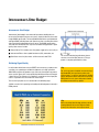
Interconnect Jitter Budget
Interconnect Jitter Budget
Interconnect jitter budget is the amount of interconnect loading that can
occur on the link before bit errors occur and is simply the ideal receiver noise
margin tRNMI specification. The latest DS92LV16 datasheets specify both left
and right tRNMI, indicating how much jitter the receiver can tolerate on either
side of the ideal bit edge before bit errors occur. The tRNMI specifications
also allow the construction of an eye mask to validate the application’s signal
quality. Jitter sources include:
■ External Noise: This includes excessive power supply noise, cross talk, etc.
■ Interconnect Effects: Inter-symbol interference (ISI), attenuation, etc.
■ Clock Jitter: excessive jitter on the serializer transmit clock TCLK.
This section of the design guide shows how to
construct a receiver input jitter mask. This eye
pattern is computer-generated for clarity.
Validating Signal Quality
In conjunction with bit error rate test (BERT) measurements, eye pattern measurements are a good way to validate the robustness of a high speed link.
While BER tests generally produce a pass/fail result, viewing the eye pattern
at the receiver inputs gives a more qualitative indication of how much margin
a given link has. The amount of “eye opening” around the receiver input jitter
mask is a qualitative measure of the link’s noise margin.
The receiver input jitter mask is constructed in the following steps:
! Tip
The serial eye pattern should be measured using a
high bandwidth, low capacitance probe at the
receiver inputs, i.e. after the interconnect’s loading
effects (backplane and/or cable) have occurred. A
PRBS pattern or real system data pattern should
be used to construct the eye pattern.
1) Make sure the link is operating and sending the desired pattern (normally a
PRBS pattern).
! Tip
When calculating ideal bit edge positions, do not
round up/down to the nearest 10 picoseconds.
Instead, calculate to the nearest picosecond.
15
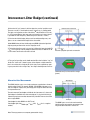
Interconnect Jitter Budget (continued)
2) Capture the entire eye pattern at the receiver inputs using a high bandwidth oscilloscope in variable persistence mode with a high
speed (> 1 GHz), high impedance (> 100 kΩ) differential probe. The TCLK signal should be used as the trigger.
Full eye pattern captured by the scope set to variable persistence mode.
3) Use the vertical cursor function of the scope to place a vertical cursor over the average 0V differential crossing point of the clock0-bit/clock-1-bit low-to-high transition. This cursor position is now the ideal time point to which all other positions will be referenced.
Ideal bit edge positions are always multiples of T/18 away from the ideal clock0-clock1 low to high transition.
The receiver jitter margin for any bit on the eye pattern can be calculated based on its ideal bit edge positions.
16
Note: These eye patterns are computer-generated for clarity.
Interconnect Jitter Budget (continued)
4) Select the bit “eye” pattern in which to place the receiver input jitter mask.
The worst case bit, i.e. the bit with the most “closed” eye, is recommended.
The ideal crossing points on either side of the nth data bit will be n*T/18 and
(n+1)*T/18 away from the ideal stop-start crossing point set in step 3, where T
is period of the TCLK frequency. (16 data bits plus 2 clock bits = 18 bits.)
5) Calculate the ideal bit edges, being careful to avoid rounding errors, and
place a cursor at both ideal bit edges of the selected bit.
6) Add tRNMI-left to the ideal left bit edge and tRNMI-right to the right ideal
edge to get the positions of the receiver input jitter mask.
7) The height of the jitter mask is the receiver’s differential input threshold VTH
- VTL. This is typically ± 50 mV, though the datasheet value of ± 100 mV can be
used if a more conservative estimate is desired.
Receiver input jitter eye mask construction.
8) The receiver input jitter mask should now look like a box inside the “eye” of
the bit. The “white area” (shown in green in the diagram at right) around the
box is the relative noise margin of the link. As long as the captured eye opening stays out of this noise margin “box,” the chipset should operate error-free.
Qualitative analysis of interconnect margin
(green).
Alternative Jitter Measurements
The tRNMI-left/right specs can also be used to get a quantitative estimate of
remaining jitter margin. The quantity (tRNMI - jitter)/tRNMI of the worst case
side (see diagram at right) is the percentage jitter margin left before bit errors
are expected to occur.
The total amount of jitter budget available for the interconnect (i.e. how much
jitter budget is allowed for the cable or backplane) is calculated similarly by
subtracting maximum transmitter deterministic jitter tDJIT from receiver ideal
noise margin tRNMI:
Jitter budget left side: tRNMI-left - tDJIT (max)
Jitter budget right side: tRNMI-right + tDJIT (min) {tDJIT min is a negative
number}
Note: These eye patterns are computer-generated for clarity.
The tRNMI specs can also be used around the
ideal bit position to guage the percentage of jitter
margin left before bit errors could occur.
17
Troubleshooting
Troubleshooting
The DS92LV16 is a robust, easy-to-use SerDes and application issues should
be rare. If application problems do occur, the causes can normally be traced
to a few simple, easy-to-check areas (listed in order relevance):
■ Power Supply Noise: Excessive supply noise, especially on the PLL supply
(PVCC), can add jitter to the transmitter serial output and affect the receiver
data sampling. Keep supply noise under 100 mV peak-to-peak on the PVCC
pins.
■ Transmit Clock: Minimize excessive cycle-to-cycle jitter on the transmit
clock TCLK in the range or 200 kHz - 2 MHz which can add jitter to the transmitter serial output.
■ Serial Bus: Should follow LVDS PCB layout and backplane recommendations, using proper termination, avoiding long stubs, and assuring the termination resistor is close to the receiver input.
■ Parallel Bus: The parallel LVTTL signals should not violate any setup and
hold times and should be free from excessive overshoot/undershoot.
18
Additional Technical Resources
National Semiconductor LVDS Feature Web Site
www.national.com/lvds is a one-stop-shop for device information and technical information such as application notes, white papers, the LVDS Owner’s
Manual, evaluation board documentation, IBIS models, frequently-askedquestions, online seminar materials, and much more.
LVDS Owner’s Manual
The LVDS Owner’s Manual teaches what LVDS is, how it works, what its
advantages are, how to design with it. It should be part of every high speed
interconnect designer’s library. The LVDS Owner’s Manual can be downloaded from the web at www.national.com/lvds or ordered from one of
National’s sales representatives.
RAPIDESIGNER® Slide Rule
National Semiconductor’s Transmission Line RAPIDESIGNER Slide Rule makes
PCB stripline and microstrip transmission line calculations quick and easy.
The slide rule is available in both metric and English unit versions. Instructions
and equations are given in application note AN-905.
Contact Information
See back cover for contact information or visit www.national.com/contacts.
19
For More Information
Web
• Visit our web site at www.national.com/lvds for more technical information. For sample orders, please click on the product
name under “Product Folder.”
Email/Phone/Fax
Americas
Email:
Phone:
Fax:
Europe
Email:
Phone:
[email protected]
1-800-272-9959
1-800-737-7018
Fax:
[email protected]
Deutsch
+49 (0) 69 9508 6208
English
+44 (0) 870 24 0 2171
Français
+33 (0) 1 41 91 87 90
+49 (0) 180-530 85 86
Asia Pacific
Email:
Phone:
Fax:
[email protected]
65-2544 466
65-2504 466
Japan
Email:
Phone:
Fax:
[email protected]
81-3-5639-7560
81-3-5639-7507
Nearest Distributors
• To find your nearest distributors, please visit
www.national.com/contacts
© 2002 National Semiconductor and are registered trademarks of National Semiconductor Corporation.
All other trademarks are the property of their respective companies. All Rights Reserved.
DS92LV16 Design Guide October 2002, Revision 1.02
Changes from last revision:Corrected errors in CAT5 Cable Length versus Frequency chart on page 7.
IMPORTANT NOTICE
Texas Instruments Incorporated and its subsidiaries (TI) reserve the right to make corrections, modifications, enhancements, improvements,
and other changes to its products and services at any time and to discontinue any product or service without notice. Customers should
obtain the latest relevant information before placing orders and should verify that such information is current and complete. All products are
sold subject to TI’s terms and conditions of sale supplied at the time of order acknowledgment.
TI warrants performance of its hardware products to the specifications applicable at the time of sale in accordance with TI’s standard
warranty. Testing and other quality control techniques are used to the extent TI deems necessary to support this warranty. Except where
mandated by government requirements, testing of all parameters of each product is not necessarily performed.
TI assumes no liability for applications assistance or customer product design. Customers are responsible for their products and
applications using TI components. To minimize the risks associated with customer products and applications, customers should provide
adequate design and operating safeguards.
TI does not warrant or represent that any license, either express or implied, is granted under any TI patent right, copyright, mask work right,
or other TI intellectual property right relating to any combination, machine, or process in which TI products or services are used. Information
published by TI regarding third-party products or services does not constitute a license from TI to use such products or services or a
warranty or endorsement thereof. Use of such information may require a license from a third party under the patents or other intellectual
property of the third party, or a license from TI under the patents or other intellectual property of TI.
Reproduction of TI information in TI data books or data sheets is permissible only if reproduction is without alteration and is accompanied
by all associated warranties, conditions, limitations, and notices. Reproduction of this information with alteration is an unfair and deceptive
business practice. TI is not responsible or liable for such altered documentation. Information of third parties may be subject to additional
restrictions.
Resale of TI products or services with statements different from or beyond the parameters stated by TI for that product or service voids all
express and any implied warranties for the associated TI product or service and is an unfair and deceptive business practice. TI is not
responsible or liable for any such statements.
TI products are not authorized for use in safety-critical applications (such as life support) where a failure of the TI product would reasonably
be expected to cause severe personal injury or death, unless officers of the parties have executed an agreement specifically governing
such use. Buyers represent that they have all necessary expertise in the safety and regulatory ramifications of their applications, and
acknowledge and agree that they are solely responsible for all legal, regulatory and safety-related requirements concerning their products
and any use of TI products in such safety-critical applications, notwithstanding any applications-related information or support that may be
provided by TI. Further, Buyers must fully indemnify TI and its representatives against any damages arising out of the use of TI products in
such safety-critical applications.
TI products are neither designed nor intended for use in military/aerospace applications or environments unless the TI products are
specifically designated by TI as military-grade or "enhanced plastic." Only products designated by TI as military-grade meet military
specifications. Buyers acknowledge and agree that any such use of TI products which TI has not designated as military-grade is solely at
the Buyer's risk, and that they are solely responsible for compliance with all legal and regulatory requirements in connection with such use.
TI products are neither designed nor intended for use in automotive applications or environments unless the specific TI products are
designated by TI as compliant with ISO/TS 16949 requirements. Buyers acknowledge and agree that, if they use any non-designated
products in automotive applications, TI will not be responsible for any failure to meet such requirements.
Following are URLs where you can obtain information on other Texas Instruments products and application solutions:
Products
Applications
Audio
www.ti.com/audio
Communications and Telecom www.ti.com/communications
Amplifiers
amplifier.ti.com
Computers and Peripherals
www.ti.com/computers
Data Converters
dataconverter.ti.com
Consumer Electronics
www.ti.com/consumer-apps
DLP® Products
www.dlp.com
Energy and Lighting
www.ti.com/energy
DSP
dsp.ti.com
Industrial
www.ti.com/industrial
Clocks and Timers
www.ti.com/clocks
Medical
www.ti.com/medical
Interface
interface.ti.com
Security
www.ti.com/security
Logic
logic.ti.com
Space, Avionics and Defense
www.ti.com/space-avionics-defense
Power Mgmt
power.ti.com
Transportation and Automotive www.ti.com/automotive
Microcontrollers
microcontroller.ti.com
Video and Imaging
RFID
www.ti-rfid.com
OMAP Mobile Processors
www.ti.com/omap
Wireless Connectivity
www.ti.com/wirelessconnectivity
TI E2E Community Home Page
www.ti.com/video
e2e.ti.com
Mailing Address: Texas Instruments, Post Office Box 655303, Dallas, Texas 75265
Copyright © 2011, Texas Instruments Incorporated