1
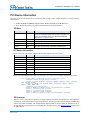
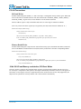
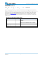
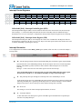
PCI-104 to PC/104 Adapter User‟s Manual PCI Device Information The PCI-104 to PC/104 Adapter has a PCI interface with 5 BAR‟s (Base Address Registers), with the following characteristics: BAR0 and BAR4 are Memory mapped; BAR1, BAR2, and BAR3 are in PCI I/O space. Byte, Word or Dword accesses, unless indicated otherwise in the details below. PCI Bars Bar Number Size (bytes) Comment(s) “0” (zero) 64K Configuration registers, used to modify and retrieve configuration info for PC/104 and EEPROM interfaces. GPIO configuration and data is also in the BAR0 register bank. Accessed as Dwords only, Register configuration below. “1” (one) 256 ISA I/O BAR_1 “2” (two) 256 ISA I/O BAR_2 “3” (three) 256 ISA I/O BAR_3 “4” (four) 16M MEM_BAR, mapped directly to ISA Memory Address space. PCI Device Information The PCI-104 to PC/104 Adapter will have the following properties in a PCI system. ID Value Comment(s) Vendor 0x12C4 Connect Tech Inc. PCI ID Device 0x1400 The PCI-104 to PC/104 Adapter Device ID Revision 0x41 (“A”) Revision of FPGA firmware Sub Vendor 0x12C4 Connect Tech Inc‟s ID Sub Device 0x1400 The ID for this board assembly Base Class 0x06 “Bridge Devices” Sub Class 0x80 “Other bridge device” Interface 0x00 Below is the output from the lspci utility in Linux with a PCI-104 to PC/104 Adapter installed in the system: 02:00.0 Bridge [0680]: Connect Tech Inc Device [12c4:1400] (rev 41) Subsystem: Connect Tech Inc Device [12c4:0000] Control: I/O+ Mem+ BusMaster- SpecCycle- MemWINV- VGASnoop- ParErr- SteppingSERR- FastB2B- DisINTxStatus: Cap+ 66MHz- UDF- FastB2B- ParErr- DEVSEL=slow >TAbort- <TAbort<MAbort- >SERR- <PERR- INTxInterrupt: pin A routed to IRQ 5 Region 0: Memory at feaf0000 (32-bit, non-prefetchable) [size=64K] Region 1: I/O ports at df00 [size=256] Region 2: I/O ports at de00 [size=256] Region 3: I/O ports at dd00 [size=256] Region 4: Memory at fd000000 (32-bit, non-prefetchable) [size=16M] PCI Interrupt The PCI-104 to PC/104 Adapter operates as a “Single function” PCI device, and therefore the card implements one interrupt, located on the INTA# signal of the PCI Bus. The interrupt is driven from multiple maskable IRQ sources from within the FPGA. The Interrupt Enable Register (IER) is used to enable the detection of the 11 PC/104 IRQ lines and generate the corresponding PCI Interrupt. Refer to the Interrupt Control section below for further details. Revision: 0.00 Page 8 of 19 Date: June 22, 2012