Download Xtreme I/O ADC-DAC - Connect Tech Inc.
Transcript
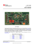
Xtreme I/O Express ADC-DAC User Manual Connect Tech Inc. 42 Arrow Road Guelph, Ontario N1K 1S6 Tel: Toll: Fax: Email: Web: 519-836-1291 800-426-8979 (North America only) 519-836-4878 [email protected] [email protected] www.connecttech.com CTIM-00435 Revision (v005) – 05/19/2015 Revision (v005) 1 Connect Tech Xtreme I/O Express ADC-DAC Family User Manual Limited Lifetime Warranty Connect Tech Inc. provides a lifetime warranty for all of our products. Should this product, in Connect Tech Inc.’s opinion, fail to be in good working order during the warranty period, Connect Tech Inc. will, at its option, repair or replace this product at no charge, provided that the product has not been subjected to abuse, misuse, accident, disaster or non Connect Tech Inc. authorized modification or repair. You may obtain warranty service by delivering this product to an authorized Connect Tech Inc. business partner or directly to Connect Tech Inc. along with proof of purchase. Product returned to Connect Tech Inc. must be pre-authorized by Connect Tech Inc. with an RMA (Return Material Authorization) number marked on the outside of the package and sent prepaid, insured and packaged for safe shipment. Connect Tech Inc. will return this product by prepaid ground shipment service. The Connect Tech Inc. lifetime warranty is defined as the serviceable life of the product. This is defined as the period during which all components are available. Should the product prove to be irreparable, Connect Tech Inc. reserves the right to substitute an equivalent product if available or to retract lifetime warranty if no replacement is available. The above warranty is the only warranty authorized by Connect Tech Inc. Under no circumstances will Connect Tech Inc. be liable in any way for any damages, including any lost profits, lost savings or other incidental or consequential damages arising out of the use of, or inability to use, such product. Copyright Notice The information contained in this document is subject to change without notice. Connect Tech Inc. shall not be liable for errors contained herein or for incidental consequential damages in connection with the furnishing, performance, or use of this material. This document contains proprietary information that is protected by copyright. All rights are reserved. No part of this document may be photocopied, reproduced, or translated to another language without the prior written consent of Connect Tech Inc. Copyright 2015 by Connect Tech Inc. Trademark Acknowledgment Connect Tech Inc. acknowledges all trademarks, registered trademarks and/or copyrights referred to in this document as the property of their respective owners. Not listing all possible trademarks or copyright acknowledgments does not constitute a lack of acknowledgment to the rightful owners of the trademarks and copyrights mentioned in this document. 2 Revision (v005) Connect Tech Xtreme I/O Express ADC-DAC User Manual Table of Contents Limited Lifetime Warranty ............................................................................................................................................... 2 Copyright Notice............................................................................................................................................................... 2 Trademark Acknowledgment ............................................................................................................................................ 2 Table of Contents .............................................................................................................................................................. 3 Revision History ............................................................................................................................................................... 3 Customer Support Overview ............................................................................................................................................. 4 Contact Information .......................................................................................................................................................... 4 Introduction....................................................................................................................................................................... 5 Product Specifcations........................................................................................................................................................ 5 Board Diagram .................................................................................................................................................................. 6 Block Diagram .................................................................................................................................................................. 7 Part Number Information .................................................................................................................................................. 8 General Board Operation .................................................................................................................................................. 9 Interfacing Convention ......................................................................................................................... 9 Top Level Registers .............................................................................................................................. 9 Analog Inputs (ADC’s) ................................................................................................................................................... 10 Overview ........................................................................................................................................... 10 ADC Connector (P4) Pinout ................................................................................................................ 10 ADC Detailed Information .................................................................................................................. 11 Registers ........................................................................................................................................... 12 ADC Transfer Function / Code Conversions ......................................................................................... 14 Application Examples ......................................................................................................................... 15 Analog Outputs (DAC’s) ................................................................................................................................................ 17 Overview ........................................................................................................................................... 17 DAC Connector (P7) Pinout ................................................................................................................ 17 DAC Detailed Information .................................................................................................................. 18 Registers ........................................................................................................................................... 21 DAC Transfer Functions ..................................................................................................................... 24 Application Examples ......................................................................................................................... 25 GPIO (Digital I/O) .......................................................................................................................................................... 26 Overview ........................................................................................................................................... 26 GPIO Connector (P3) Pinout .............................................................................................................. 26 GPIO Operation ................................................................................................................................ 27 PCIe/104 Information ..................................................................................................................................................... 28 Device Software / Configuration Information ................................................................................................................. 29 PCI Device Information ...................................................................................................................... 29 Board ID Registers ............................................................................................................................. 29 SPI Program Flash Controller............................................................................................................. 29 Complete Memory Map ....................................................................................................................... 30 Revision History Revision Date Author(s) Change(s) Prelim-v001 02-10-2015 PD Initial Manual Revision Created V002 02-19-2015 PD Updated with Core Content V003 05-14-2015 AS Updated to reflect new firmware revision V004 05-19-2015 AS Finished Signal Gen Section V005 05-25-2015 AS Finished PWM Section Revision (v005) 3 Connect Tech Xtreme I/O Express ADC-DAC Family User Manual Customer Support Overview If you experience difficulties after reading the manual and/or using the product, contact the Connect Tech Inc. reseller from which you purchased the product. In most cases the reseller can help you with product installation and difficulties. In the event that the reseller is unable to resolve your problem, our highly qualified support staff can assist you. Our support section is available 24 hours a day, 7 days a week on our website at: www.connecttech.com/sub/support/support.asp. See the contact information section below for more information on how to contact us directly. Our technical support is always free. Contact Information We offer three ways for you to contact us: Mail/Courier You may contact us by letter at: Connect Tech Inc. Technical Support 42 Arrow Road, Guelph, ON Canada N1K 1S6 Email/Internet You may contact us through the Internet. Our email and URL addresses on the Internet are: [email protected] [email protected] www.connecttech.com Note: Please go to the Download Zone or the Knowledge Database in the Support Center on the Connect Tech Inc. website for product manuals, installation guides, device driver software and technical tips. Submit your technical support questions to our customer support engineers via the Support Center on the Connect Tech Inc. website. Telephone/Facsimile Technical Support representatives are ready to answer your call Monday through Friday, from 8:30 a.m. to 5:00 p.m. Eastern Standard Time. Our numbers for calls are: Telephone: Telephone: Facsimile: 4 800-426-8979 (North America only) 519-836-1291 (Live assistance available 8:30 a.m. to 5:00 p.m. EST, Monday to Friday) 519-836-4878 (online 24 hours) Revision (v005) Connect Tech Xtreme I/O Express ADC-DAC User Manual Introduction Connect Tech’s Xtreme I/O Express ADC-DAC is an analog and digital peripheral board for the PCI-104 small form factor embedded marketplace. This product is ideal for data acquisition, measurement and control applications. Product Specifcations Specification Details Form Factor PCIe/104 or PCI/104-Express Fully Analog Inputs Channels: 32 Single Ended Resolution: 16-bit Sampling Rate: 500ksps Protection: ±20V Input Ranges: o Bipolar: ±10.24V, ±5.12V and ±2.56V o Unipolar: 0 - 10.24V and 0 - 5.12V Accuracy: ±2.5 LSB INL, ±1.5 LSB DNL Signal-to-Noise Ratio: 91 dB @ ±10.24V Analog Outputs Channels: 4 Resolution: 16-bit Output Ranges: Six Programmable Output Ranges o Unipolar: 0V to 5V, 0V to 10V o Bipolar: ±5V, ±10V, ±2.5V, –2.5V to 7.5V Accuracy: 1LSB INL and DNL Settling Time: 6µs Outputs Drive: ±3mA Digital I/O Channels: 16-bit bidirectional I/O Input/Output Ranges: Hardware selectable +3.3V or +5V(TTL/CMOS) Output Drive: High Current 24mA Controller FPGA Register Controlled Device (No jumpers needed) Custom logic available upon request Operating Temperature -40 to +85 Degrees Celsius Dimensions 3.775” x 3.550” (PC/104 Compliant) Host Interface Bus PCI Express Gen 1.0/2.0 bus compliant (PCIe/104) (PCI-104) connector can be optionally installed as a pass-through connector Power Details +5VDC only operation (all on-board voltages are made from the +5V rail) Current Consumption (800mA peak, 500mA typical) Software Compatibility Custom CTI Device Drivers for QNX, Linux, Windows Device can also be controlled directly from a memory mapped register set in any operating system Warranty and Support Lifetime Warranty Free Technical Support Revision (v005) 5 Connect Tech Xtreme I/O Express ADC-DAC Family User Manual Board Diagram 6 Revision (v005) Connect Tech Xtreme I/O Express ADC-DAC User Manual Block Diagram Revision (v005) 7 Connect Tech Xtreme I/O Express ADC-DAC Family User Manual Part Number Information Part Number Features DAG103 Analog Inputs : 16-bit 32 SE Analog Outputs : 16-bit 4 Channels GPIO : 16-bits DAG104 Analog Inputs : 16-bit 32 SE Analog Outputs : none GPIO : 16-bits DAG106 Analog Inputs : 16-bit 32 SE Analog Outputs : 16-bit 4 Channels GPIO : 16-bits Humiseal 1B31 Conformal Coating Board Image Photo Coming Soon To order any of these part numbers or to inquire about the other available ordering options please contact [email protected] for further information. 8 Revision (v005) Connect Tech Xtreme I/O Express ADC-DAC User Manual General Board Operation Interfacing Convention Fundamentally, all the boards in the DAG10X series operate under the principle of a register based interface. As such, in the terms of interfacing, each controller block (ADC, DAC, GPIO) can be seen as being represented by a range of register banks located at constant offsets from a base memory address. Inducing an action in one of the controller blocks involves simply writing/reading a value(s) to/from the pertinent memory address(es). The smallest addressable unit of memory supported by the controller blocks in these transactions is eight bits and the largest is thirty-two bits. Memory Map 32-bits General Board Control 0x1000 ADC0 0x4000 ADC1 0x7000 ADC2 0xA000 ADC3 0xD000 DAC 0x10000 0x10009 GPIO Reserved/Internal 0x24210 System ID/Time Stamp Top Level Registers General Board Control Offset (Dec) Offset (Hex) 0 0x0 0x03 0x02 0x01 4 0x4 Reserved / Future Use 8 0x8 LEDMODE: bit 1 low(default): slow pulse, bit 1 high: Compare_Value match 0x00 Reserved / Future Use 12 0xC IRQ_STATUS: lower four bit hold IRQ flags for the ADC sample FIFOs 16 0x10 Compare_Mask: This values is ANDed with Compare_Value and read value before comparison 20 0x14 Compare_Value: Value to compare against last read value 24 0x18 SCRATCHPAD REG-1 28 0x1C SCRATCHPAD REG-2 Only the IRQ_STATUS register is really relevant for general usage of the board and the rest of the values can be safely ignored. The ADC controller blocks will set bits in this register when they are in Waveform Capture Mode (See the ADC section for more information). Revision (v005) 9 Connect Tech Xtreme I/O Express ADC-DAC Family User Manual Analog Inputs (ADC’s) Overview The Xtreme I/O Express ADC-DAC use 4 ADC IC’s which are interfaced to the on-board FPGA. Each of these ADC IC’s have an 8-channel multiplexer that allow for the sampling of 8 single ended channels. ADC IC Features and Specifications Part Number: ADS8688 (Texas Instruments) Resolution: 16-bit Sample Rate: 500ksps 8-Channel Multiplexer with ±20V Protection Software-Programmable Input Ranges: o Bipolar: ±10.24 V, ±5.12 V, and ±2.56 V o Unipolar: 0 V to 10.24 V and 0 V to 5.12 V DNL: ±0.5 LSB; INL: ±0.75 LSB SNR: 92 dB; THD: –102 dB Power Dissipation: 65mW (Typ) The ADC IC datasheet can be found here: http://www.ti.com/lit/gpn/ads8688 ADC Connector (P4) Pinout Pinout Table Signal ADC0 CH-0 ADC0 CH-2 ADC0 CH-4 ADC0 CH-6 GND ADC1 CH-0 ADC1 CH-2 ADC1 CH-4 ADC1 CH-6 GND ADC2 CH-0 ADC2 CH-2 ADC2 CH-4 ADC2 CH-6 GND ADC3 CH-0 ADC3 CH-2 ADC3 CH-4 ADC3 CH-6 GND Connector Location HDR Pin 1 3 5 7 9 11 13 15 17 19 21 23 25 27 29 31 33 35 37 39 HDR Pin 2 4 6 8 10 12 14 16 18 20 22 24 26 28 30 32 34 36 38 40 Signal ADC0 CH-1 ADC0 CH-3 ADC0 CH-5 ADC0 CH-7 GND ADC1 CH-1 ADC1 CH-3 ADC1 CH-5 ADC1 CH-7 GND ADC2 CH-1 ADC2 CH-3 ADC2 CH-5 ADC2 CH-7 GND ADC3 CH-1 ADC3 CH-3 ADC3 CH-5 ADC3 CH-7 GND Note: Single ended readings are referenced to the GND pins on the P4 connector. Pinout Diagram (“Right” Side View of Board) – Note: Pin1 is closest to the PCB surface and Pin2 is “above” Pin1 when looking at the pins from a side profile view. 10 Revision (v005) Connect Tech Xtreme I/O Express ADC-DAC User Manual ADC Detailed Information The ADCs are controlled and have their data stored in 4 ADC# Blocks. ADC0 Block begins at offset 0x1000, ADC1 at 0x4000, ADC2 at 0x7000 and ADC3 at 0xA000. At the time of the release of this manual (BOARD ID / LOGIC RELEASE VERSION = 0x12C40002), the ADC mode of capture can be set to either Continuous Sampling Mode or Waveform Capture Mode. The input range for each of the 4 ADCs can be changed via the INPUT_RANGE_SELECT register. Each ADC block can be set to capture up to 8 channels in a looping sequential order. For example, if all eight channels were enabled in ADC0 (writing 0xFF to 0x1000) then the following shows the process it would go through in obtaining the requested samples: CH 0 CH 1 CH 3 CH 4 CH 5 CH 6 CH 7 By default sample collection occurs at the maximum sampling rate of the ADC IC which is 500ksps, so if, in continuing the previous example, all 8 channels were to be enabled then the actual sampling rate per ADC Channel would be 500ksps/8=62.5ksps. mem block M last samples setup/config ADC0 Block Offset (Dec) Offset (Hex) 4096 0x1000 0x03 0x02 CONTROL_CONFIG 4100 0x1004 Reserved / Future Use 4104 0x1008 Reserved / Future Use 4108 0x100C CLK_DIV_CNTR 4112 0x1010 INPUT_RANGE_SELECT 4116 0x1014 CH1-LAST_SAMPLE CH0-LAST_SAMPLE 4120 0x1018 CH3-LAST_SAMPLE CH2-LAST_SAMPLE 4124 0x101C CH5-LAST_SAMPLE CH4-LAST_SAMPLE 4128 0x1020 CH7-LAST_SAMPLE 0x1024 0x01 0x00 CH6-LAST_SAMPLE Mem Write Control 8192 0x2000 CHANNEL_ID/TIMESTAMP_0 MEM_SAMPLE_0 8196 0x2004 CHANNEL_ID/TIMESTAMP_1 MEM_SAMPLE_1 8200 0x2008 CHANNEL_ID/TIMESTAMP_2 MEM_SAMPLE_2 … … … … 16380 0x3FFC CHANNEL_ID/TIMESTAMP_4k MEM_SAMPLE_2k Continuous Sampling Mode Then each ADC channel’s code is captured and stored into their CHX-LAST_SAMPLE register. This CHX-LAST_SAMPLE register is then constantly updated/overwritten with a latest/newest code received. Waveform Capture Mode (FIFO Mode) The purpose of this mode is to provide a much larger degree of persistence to the data captured at the firmware level by means of a per-ADC Block sample FIFO. It can be seen as being supplementary to the Contiguous Sampling Mode in that the ADC Blocks set to operate as such will continue to update their CHX-LAST_SAMPLE registers in addition to now also storing data in their associated sample FIFOs. An ADC block operating in this mode will signal that its FIFO memory is almost full via a PCIe interrupt; the sample count at which this notification is made can be adjusted to any value within the sample depth range supported by the sample FIFOs (2047), allowing for a degree of flexibility in the granularity of the data chunks collected. It should also be noted that each time a sample is stored in one of these FIFOs it is saved along with two additional bookkeeping data fields. The first of these fields shows the channel from which the data was collected and the second shows the current position within the given FIFO’s memory space at which the save is currently being made. Revision (v005) 11 Connect Tech Xtreme I/O Express ADC-DAC Family User Manual CHANNEL_ID/TIMESTAMP_0 FIFO_SAMPLE_0 31 30 29 28 27 26 25 24 23 22 21 20 19 18 17 16 15 14 13 12 11 10 9 8 7 6 5 11-bit "Timestamp"/Sample Num R Channel ID 16-bit CODE from ADC 4 3 2 1 0 For example to set up an ADC block to capture data in its sample FIFO and provide a notification once it has stored 1023 of these values, one would write 0x3FF to the first ten bits of its MEM Write Control register and then set the MEM Store flag in its control register. Variable Sampling Rate As already touched upon the default sampling rate of the ADC blocks is 500ksps or the maximum rate supported by the ADC peripherals. If slower sampling rates are required, then each block can be individually set to subdivide this maximum rate by way of a counter roll over value stored in the CLK_DIV_CNTR register. Essentially, if sample rate division is enabled with bit number nine in the control register of an ADC block then an internal counter is incremented to the value stored in CLK_DIV_CNTR and then reset, continuously, at the maximum sampling rate. The actual subdividing of the sample rate then is, in this sense, achieved by storing new values only when the counter is equal to zero. Registers MEM Write Control (Offsets 0x1024, 0x4024, 0x7024, 0xA024) – Read/Write(Partial) MEM Write Control 31 30 29 28 27 26 25 24 23 22 21 20 19 18 17 16 15 14 13 12 11 10 Reserved / Future Use 9 8 Current FIFO Write Count 7 6 5 4 3 2 1 0 Trigger IRQ at FIFO Count Current FIFO Write Count Shows the current position in the FIFO memory (Read Only) Trigger IRQ at FIFO Count Sets the position in the FIFO memory at which the almost full IRQ is triggered (value must be greater than zero to fire) INPUT_RANGE_SELECT (Offsets 0x1010, 0x4010, 0x7010, 0xA010) – Read/Write INPUT_RANGE_SELECT 31 30 29 28 27 26 25 24 23 22 21 20 19 18 17 16 15 14 13 12 11 10 Reserved 9 8 7 6 5 4 3 2 1 0 CH7 Range CH6 Range CH5 Range CH4 Range CH3 Range CH2 Range CH1 Range CH0 Range This register contains all of the channel input range values which are described below. CHx Range [2:0] Postive Full Scale (V) Negative Full Scale (V) Full-Scale Range (V) 000 10.24 -10.24 20.48 001 5.12 -5.12 10.24 010 2.56 -2.56 5.12 101 10.24 0 10.24 110 5.12 0 5.12 LSB (µV) 312.5 156.25 78.125 156.25 78.125 CHx_LAST_SAMPLE (Offset 0x1014, 0x1016…, 0x4014, 0x4016…) – Read Only CHx_LAST_SAMPLE 15 14 13 12 11 10 9 8 7 6 5 4 3 2 1 0 CHx 16-bit CODE This register contains the last sampled 16-bit code for the specific channel. Bit-15 is the MSB of the CODE and Bit-0 is the LSB for the CODE. See the transfer function section below for details on how this code represents the voltage sampled. 12 Revision (v005) Connect Tech Xtreme I/O Express ADC-DAC User Manual CONTROL_CONFIG (Offset 0x1000, 0x4000, 0x7000, 0xA000) - Read/Write CONTROL_CONFIG 31 30 29 28 27 26 25 24 23 22 21 20 19 18 17 16 15 14 13 12 11 10 Reserved / Future Use Mode 9 8 7 6 5 4 3 2 1 Channel Enable 31 Internal: Pending write request 30 Reserved / Future Use 29 Reserved / Future Use 28 Reserved / Future Use 27 Reserved / Future Use 26 Reserved / Future Use 25 Reserved / Future Use 24 Reserved / Future Use 23 Reserved / Future Use 22 Reserved / Future Use 21 Reserved / Future Use 20 Reserved / Future Use 19 Reserved / Future Use 18 Reserved / Future Use 17 Reserved / Future Use 16 Reserved / Future Use 15 Reserved / Future Use 14 Reserved / Future Use 13 Reserved / Future Use 12 STOP - 0=normal operation, 1=stop sampling 11 Reserved / Future Use 10 RESET - 0=normal operation, 1=reset ICs and regs 9 Divide Sample Rate - 0=maximum rate, 1=divide 8 MEM Store - 1=store samples in memory, 0=don't store 7 Sample CHAN0 6 Sample CHAN1 5 Sample CHAN2 4 Sample CHAN3 3 Sample CHAN4 2 Sample CHAN5 1 Sample CHAN6 0 Sample CHAN7 Revision (v005) 13 0 Connect Tech Xtreme I/O Express ADC-DAC Family User Manual ADC Transfer Function / Code Conversions When reading the samples from the ADC’s on the Xtreme I/O Express ADC-DAC, they will be in straight binary format for both bipolar and unipolar input ranges. The format for the output codes is the same across all analog channels. The ideal transfer characteristic for each ADC channel for all input ranges is shown below. The full-scale range (FSR) for each input signal is equal to the difference between the positive fullscale (PFS) input voltage and the negative full-scale (NFS) input voltage. The LSB size is equal to FSR / 65536 because the resolution of the ADC is 16 bits. Code translation examples: Code = 0x0000 | CHx Range[2:0] = 000 | FSR = 20.48V Code = 0x8000 | CHx Range[2:0] = 000 | FSR = 20.48V Code = 0xffff | CHx Range[2:0] = 000 | FSR = 20.48V | Actual Voltage is = -10.24V | Actual Voltage is = 0.00V | Actual Voltage is = 10.24V Code = 0x0000 | CHx Range[2:0] = 001 | FSR = 10.24V Code = 0x8000 | CHx Range[2:0] = 001 | FSR = 10.24V Code = 0xffff | CHx Range[2:0] = 001 | FSR = 10.24V | Actual Voltage is = -5.12V | Actual Voltage is = 0.00V | Actual Voltage is = 5.12V Code = 0x0000 | CHx Range[2:0] = 110 | FSR = 5.12V Code = 0x8000 | CHx Range[2:0] = 110 | FSR = 5.12V Code = 0xffff | CHx Range[2:0] = 110 | FSR = 5.12V | Actual Voltage is = 0.00V | Actual Voltage is = 2.56V | Actual Voltage is = 5.12V 14 Revision (v005) Connect Tech Xtreme I/O Express ADC-DAC User Manual Application Examples ADC Operation Pseudo Code Example A In this example we will set all 4 ADC IC’s to enable sampling, and set the input range for each of the ADCs to be +/-10.24V. Then we will read back from ADC0-CH0, ADC1-CH4, ADC2-7 and ADC3-CH1. // setup input range to be +/- 10.24V for all channels on all ADCs write DWord 0x0 to offset 0x1010 //ADC0 setup write DWord 0x0 to offset 0x4010 //ADC1 setup write DWord 0x0 to offset 0x7010 //ADC2 setup write DWord 0x0 to offset 0xA010 //ADC3 setup // enable continuous sampling on all ADCs write DWord 0xff to offset 0x1000 //ADC0 setup write DWord 0xff to offset 0x4000 //ADC1 setup write DWord 0xff to offset 0x7000 //ADC2 setup write DWord 0xff to offset 0xA000 //ADC3 setup //read from ADC0-CH0 ADC0-CH0_code = read //read from ADC1-CH4 ADC1-CH4_code = read //read from ADC2-CH7 ADC2-CH7_code = read //read from ADC3-CH1 ADC3-CH1_code = read Word from offset 0x1014 Word from offset 0x401c Word from offset 0x7022 Word from offset 0xA016 ADC Operation Pseudo Code Example B In this example we will set: - ADC0 to take a readings from CH0 with an input voltage range of +/-10.24V - ADC1 to take a readings from CH0 with an input voltage range of +/-5.12V - ADC2 to take a readings from CH0 with an input voltage range of 0 to +10.24V - ADC3 to take a readings from CH0 with an input voltage range of 0 to +5.12V Then every 50ms (using a real time OS) we will store a sample. // setup all ADC0 channels with an input write DWord 0x0 to offset 0x1010 // setup all ADC1 channels with an input write DWord 0x249249 to offset 0x4010 // setup all ADC2 channels with an input write DWord 0xB6DB6D to offset 0x7010 // setup all ADC3 channels with an input write DWord 0xDB6DB6 to offset 0xA010 range of +/-10.24V range of +/-5.12V range of 0 to +10.24V range of 0 to +5.12V // enable continuous sampling on all ADCs write DWord 0xff to offset 0x1000 //ADC0 setup write DWord 0xff to offset 0x3000 //ADC1 setup write DWord 0xff to offset 0x4000 //ADC2 setup write DWord 0xff to offset 0x7000 //ADC3 setup //start reading channels in a loop loop //read from ADC0 ADC0-CH0_code = read Word from //read from ADC1 ADC1-CH0_code = read Word from //read from ADC2 ADC2-CH0_code = read Word from //read from ADC3 ADC3-CH0_code = read Word from wait 50ms end loop Revision (v005) offset 0x1014 offset 0x3014 offset 0x5014 offset 0x7014 15 Connect Tech Xtreme I/O Express ADC-DAC Family User Manual ADC Operation Pseudo Code Example C In the final ADC example we will place ADC0 into Waveform Capture Mode, request that it only receives samples from channel 0 and finally notify it that we want to be informed once it has received 2047 samples. We will then wait for an interrupt and once one is received we will then dump all the data accumulated in the sample FIFO through a loop. // setup all ADC0 channels with an input range of +/-10.24V write DWord 0x0 to offset 0x1010 // Set interrupt to fire once 2047 samples have been stored write DWord 0x7FF to offset 0x1024 // Switch to Waveform Capture Mode and enable only channel 0 write DWord 0x180 to offset 0x1000 // Wait for interrupt waitforirq bit 0 at offset 0xC // Clear interrupt write DWord 0x0 to offset 0xC // Disable all capture write DWord 0x0 to offset 0x1000 // Dump all of the data stored in the FIFO loop while i < 2047 adc0_code_array i = read bits 15 – 0 from offset 0x2000 i = i + 1; end loop 16 Revision (v005) Connect Tech Xtreme I/O Express ADC-DAC User Manual Analog Outputs (DAC’s) Overview The Xtreme I/O Express ADC-DAC uses a 16-bit 4-channel DAC IC which is interfaced to the on-board FPGA. ADC IC Features and Specifications Part Number: DAC8734 (Texas Instruments) Resolution: 16-bit Channels: 4 Settling Time: 6µs Output Ranges: o Unipolar: 0V to 15V o Bipolar: ±10V Accuracy: 1LSB INL and DNL Settling Time: 6µs Outputs Drive: ±3mA The DAC IC datasheet can be found here: http://www.ti.com/lit/gpn/dac8734 DAC Connector (P7) Pinout Pinout Table Signal DAC_OUTA DAC_OUTB DAC_OUTC DAC_OUTD GND Connector Location HDR Pin 1 3 5 7 9 HDR Pin 2 4 6 8 10 Signal GND GND GND GND GND Pinout Diagram (“Left” Side View of Board) Note: Pin1 is closest to the PCB surface and Pin2 is “above” Pin1 when looking at the pins from a side profile view. Revision (v005) 17 Connect Tech Xtreme I/O Express ADC-DAC Family User Manual DAC Detailed Information The DAC8734 IC has 4 DAC outputs DAC0,1,2 and 3. The DAC block can be configured to drive the DAC peripheral from one of three sources, direct software writes (Direct Write Mode), block ram stored sequences (Signal Gen Mode) or a built in PWM (PWM Mode). On power on the DAC defaults to the first mode but can easily be switched to one of the other two by writing to the appropriate bits in the Trigger SigGen/PWM register. mem block setup/config DAC0 Block Offset (Dec) Offset (Hex) 53248 0xD000 0x03 0x02 0x01 0x00 53252 0xD004 DAC1 - DATA 53256 0xD008 DAC3 - DATA 53260 0xD00C DAC0 - ZERO REG / GAIN REG 53264 0xD010 DAC1 - ZERO REG / GAIN REG 53268 0xD014 DAC2 - ZERO REG / GAIN REG 53272 0xD018 DAC3 - ZERO REG / GAIN REG 53276 0xD01C DAC_IO_PINS_CONTROL 53280 0xD020 DAC_COMMAND_PASSTHRU 53284 0xD024 Trigger SigGen/PWM 53288 0xD028 53292 0xD02C PWM High Count 53296 0xD030 Reserved / Future Use 53300 0xD034 PWM High Value 53304 0xD038 57344 0xE000 MEM_SAMPLE_0 MEM_SAMPLE_1 57348 0xE004 MEM_SAMPLE_2 MEM_SAMPLE_3 57352 0xE008 MEM_SAMPLE_4 MEM_SAMPLE_5 … … … … 65532 0xFFFC MEM_SAMPLE_2k-1 MEM_SAMPLE_2k DAC_CONTROL_CONFIG DAC0 - DATA DAC2 - DATA SigGen Read Control PWM Low Count PWM Frequency Factor PWM Control PWM Low Value SAMPLE_DIV_CNTR Direct Write Mode In this mode the DAC controller block listens in for writes to the registers located at 0xD004 and 0xD008 and then immediately sends the contents of one or the other if it detects a write has been made. A write to address 0xD004 will trigger the transmission of the new values to channel 0 and 1 and a write to address 0xD008 will trigger the transmission of the new values to channel 2 and channel 3. While the controller will always send in two channel values at a time, one can use byte enables to write just 16 bits to either the upper or lower portion of one of the Direct Write Mode data registers. When the transmission to the peripheral is then triggered the old value in the other channel slot will be rewritten with the same thing. Signal Gen Mode The purpose of this mode is to allow the board to generate arbitrary, user-defined signals through the DAC peripheral independent of any active software management. When operating in this capacity, the board will persistently source its outputs to the DAC peripheral from values stored in its associated block memory in a manner as dictated by the fields within the SigGen Read Control register. The Base Memory Address field is interpreted as the address in the block memory where the first two voltage levels of the signal to be output are stored and the Read Count field is seen as the address of the final two (as an offset from the first address). Additionally, the block controller will look to the To Chan field to determine which channel on the signal should be output to and the D flag to decide whether it should slow the signal down with the subdivision value stored in SAMPLE_DIV_CNTR. 18 Revision (v005) Connect Tech Xtreme I/O Express ADC-DAC User Manual For example, if the first address were to be set to 0x100 and the final to an offset of 0x04 then the block memory would be accessed in the following pattern: 0x100 0x101 0x102 0x103 0x104 PWM Mode The variable periods of logic ‘1’ and logic ‘0’ are controlled by the high and low data registers, respectively. The values in these registers represent the number of clock cycles in which the pulse will remain high and low. The count values are passed to the pulse generator unit, which acts as a counter and flip-flop, switching between counting up to the high and low values from 0, and toggling the output bit appropriately. The duty cycle of the pulse is controlled by the ratio of the high count to the period count (which is determined by summing the high and low count values). Moreover, the frequency of the output can be controlled by carefully selecting the count value of the period Note that both PWM A and PWM B have the same duty cycle (50%), but PWM B has a period count which is twice that of PWM A, and so its frequency will be half as much. Frequency can be controlled using: 𝐹𝑟𝑒𝑞𝑢𝑒𝑛𝑐𝑦 = 1 𝑃𝑒𝑟𝑖𝑜𝑑 𝐶𝑜𝑢𝑛𝑡 ∗ 𝐼𝑛𝑝𝑢𝑡 𝐶𝑙𝑜𝑐𝑘 𝐶𝑦𝑐𝑙𝑒 (𝑠𝑒𝑐𝑜𝑛𝑑𝑠) In order to generate a wider range of frequencies, two 8-bit registers were used for each of the high and low count values, which work in conjunction to provide 16-bits for each. In addition, to aide in the generation of very low frequencies, this design includes a frequency factor register, which conditionally acts as an extra bit for the high and low counts to further divide the input clock. Working in powers of 10, the frequency factor helps in transferring any count values which are too large to be represented by the 16-bit registers. Revision (v005) 19 Connect Tech Xtreme I/O Express ADC-DAC Family User Manual The block diagrams of the Pulse Generator and PWM unit are shown in the following two diagrams. 20 Revision (v005) Connect Tech Xtreme I/O Express ADC-DAC User Manual HIGH/LOW COUNT REGISTERS The high/low count registers control the value determining the amount of clock cycles in which the PWM output remains logic ‘1’ or logic ‘0’ respectively. They act in conjunction to form a 16-bit value, where high/low0 represents bits 0-7, and high/low1 represents bits 8-15. Registers ZERO REG/GAIN REG (Offset 0xD00C, 0xD010, 0xD014, 0xD018) – Read/Write ZERO REG/GAIN REG 31 30 29 28 27 26 25 24 23 22 21 20 19 18 17 16 15 14 13 12 11 10 Reserved / Future Use 9 8 7 6 Zero Register 5 4 3 2 1 0 1 0 Gain Register Zero Register stores user-calibration data that is used to eliminate offset error Gain Register stores user-calibration data that is used to eliminate gain error DAC_IO_PINS_CONTROL (Offset 0xD01C) – Read/Write DAC_IO_PINS_CONTROL 31 30 29 28 27 26 25 24 23 22 21 20 19 18 17 16 15 14 13 12 11 10 9 8 7 6 5 4 Reserved / Future Use 3 2 UB UA RST LD This register sets the Unipolar and Bipolar modes of the outputs for each group of DAC outputs. It is unique among all the other registers in that it is actually a direct mapping to pins on the peripheral bearing the same designations. Bit 3 – Unipolar/Bipolar B 0 = Sets DAC2 & DAC3 to Bipolar Mode (-10V to +10V) 1 = Sets DAC2 & DAC3 to Unipolar Mode (0V to +15V) Bit 2 – Unipolar/Bipolar A 0 = Sets DAC0 & DAC1 to Bipolar Mode (-10V to +10V) 1 = Sets DAC0 & DAC1 to Unipolar Mode (0V to +15V) Bit-1 – DAC Reset 0 = Take DACs output of reset (Normal Operation) 1 = Put DACs input reset state Bit-0 – Load DAC Outputs 0 = Enable DAC Updating (Normal operation) 1 = Disable DAC Updating DAC_COMMAND_PASSTHRU (Offset 0xD020) – Read/Write DAC_COMMAND_PASSTHRU 31 30 29 28 27 26 25 24 23 22 21 20 19 18 17 16 15 14 13 12 11 10 Zeros (Must always be zeros) Command Addr 9 8 7 6 5 4 3 2 1 0 Command Data This register communicates directly with the SPI connected DAC IC. Whatever data is in this register gets shifted out to the DAC IC. This allows access to the DAC IC’s internal register bank which is detailed below: Revision (v005) 21 Connect Tech Xtreme I/O Express ADC-DAC Family User Manual DAC8734 Internal Register Bank CMD ADDR DATA [15:0] 0x0 CONFIG CODE 0x4 DAC0 CODE 0x5 DAC1 CODE 0x6 DAC2 CODE 0x7 DAC3 CODE 0x8 DAC0 ZERO CODE 0x9 DAC1 ZERO CODE 0xA DAC2 ZERO CODE 0xB DAC3 ZERO CODE 0xC DAC0 GAIN CODE 0xD DAC1 GAIN CODE 0xE DAC2 GAIN CODE 0xF DAC3 GAIN CODE [DAC8734 Internal] - CONFIG_CODE – You must always set this register to 0x3C for normal operation. All other values are undefined; do not load any values other than 0x3C into this location. [DAC8734 Internal] - DACx_CODE DACx_CODE 15 14 13 12 11 10 9 8 7 6 5 4 3 2 1 0 DACx 16-bit CODE This register contains the 16-bit code for the specific DAC output (0,1,2 or 3). Bit-15=MSB, Bit-0=LSB. CODE Formats: For UNIPOLAR Mode = Straight Binary For BIPOLAR Mode = Two’s Complement Trigger SigGen/PWM (Offset 0xD024) – Read/Write Trigger SigGen/PWM 31 30 29 28 27 26 25 24 23 22 21 20 19 18 17 16 15 14 13 12 11 10 I:PAddr Reserved / Future Use Bit 1 – Advanced Mode Enable 0 = Disabled (In Direct Write Mode) 1 = Enabled Bit 0 – Advanced Mode Type 0 = Signal Gen Mode 1 = PWM Mode 9 8 9 8 7 6 5 4 3 2 1 T 0 F 7 6 5 4 3 2 Base Memory Address 1 0 SigGen Read Control (Offset 0xD028) – Read/Write SigGen Read Control 31 30 29 28 27 26 25 24 23 22 21 20 19 18 17 16 15 14 13 12 11 10 Reserved / Future Use D To Chan Read Count Base Memory Address Memory address containing the first encoded voltage level of the signal to be output Read Count Length of the signal to be output (effectively then the address of the last voltage level output is Base Memory Address + Read Count) To Chan Channel to send generated signal output to Bit 24 – Sample Division Use SAMPLE_DIV_CNTR value to subdivide the output frequency of the generated signal 22 Revision (v005) Connect Tech Xtreme I/O Express ADC-DAC User Manual PWM Count (Offset 0xD02C) – Read/Write PWM Count 31 30 29 28 27 26 25 24 23 22 21 20 19 18 17 16 15 14 13 12 11 10 PWM High Count 9 8 7 6 5 4 3 2 1 0 PWM Low Count PWM High Count The high count registers control the value determining the amount of clock cycles in which the PWM output remains logic ‘1’ PWM Low Count The low count registers control the value determining the amount of clock cycles in which the PWM output remains logic ‘0’ PWM CONTROL/FREQ (Offset 0xD030) – Read/Write PWM Control/Freq 31 30 29 28 27 26 25 24 23 22 21 20 19 18 17 16 15 14 13 12 11 10 9 Reserved / Future Use To Chan PWM Frequency Factor 8 7 6 5 4 3 2 PWM Control 1 0 To Chan Channel to send PWM output to PWM Frequency Factor Only a value of 0x1 is currently supported at this time (no subdivision) PWM Control See table below Bit(s) Reset Value Description 0 0x0 Select high register for R/W 0=high0 1=high1 1 0x0 Select low register for R/W 0=low0 1=low1 2 0x0 Load Pulse Generator 0=Disable 1=Load 3 0x0 Enable Output 0=Disable 1=Enable 4 0x0 Pulse Generator Reset 1=Reset 5 0x0 6 0x0 7 0x0 Unused PWM High/Low Level (Offset 0xD034) – Read/Write PWM High/Low Level 31 30 29 28 27 26 25 24 23 22 21 20 19 18 17 16 15 14 13 12 11 10 High Level 9 8 7 6 Low Level 5 4 3 2 High Level The voltage level output when the PWM signal is output as high Low Level The voltage level output when the PWM signal is output as low Revision (v005) 1 0 23 Connect Tech Xtreme I/O Express ADC-DAC Family User Manual DAC Transfer Functions For Normal Operation the INPUT_CODE and ZERO_CODE registers for each of DAC outputs should be set to 0x0, see below for details on CODE formats for this case. DACx_CODE in Two’s Complement Code for Bipolar Output Operation Note: Gain=4, Vref=5 DACx_CODE in Straight Binary Code for Unipolar Output Operation Note: Vref=5. Note saturation point will be at +15V, so actually highest code will be 0xC000 [DAC8734 Internal] - DACx Zero Code The Zero Register stores the user-calibration data that are used to eliminate the offset error. The data are nine bits wide, 0.125 LSB/step, and the total adjustment is typically – 32 LSB to +31.875 LSB, or ± 0.0488% of full-scale range. The Zero Register uses a twos complement data format in both bipolar and unipolar modes of operation. 24 Revision (v005) Connect Tech Xtreme I/O Express ADC-DAC User Manual [DAC8734 Internal] - DACx Gain Code The Gain Register stores the user-calibration data that are used to eliminate the gain error. The data are eight bits wide, 1 LSB/step, and the total adjustment is typically – 128 LSB to +127 LSB, or ± 0.195% of full-scale range. The Gain Register uses a twos complement data format in both bipolar and unipolar modes of operation. Application Examples DAC Operation Pseudo Code Example A In this example we will set all of the DAC outputs to Unipolar Mode (0 to +15V), then we will set DAC0 & DAC1 to +5V, DAC2 to be +10V and DAC3 to be +15V. // setup all DAC outputs for Unipolar Mode and put in Normal Operation write DWord 0xC to offset 0xD01C //unipolar setup write DWord 0x3C to offset 0xD020 //enable normal operation write write write write DWord DWord DWord DWord 0x44000 0x54000 0x68000 0x7C000 to to to to offset offset offset offset 0xD020 0xD020 0xD020 0xD020 //Set //Set //Set //Set DAC0 DAC1 DAC2 DAC3 to to to to +5V +5V +10V +15V DAC Operation Pseudo Code Example B In this example we will set all of the DAC outputs to Bipolar Mode (-10V to +10V), then we will set DAC0 to -10V, DAC1 to -5V, DAC2 to +2.5V, DAC3 to 9V. // setup all DAC outputs for Bipolar Mode and put in Normal Operation write DWord 0x0 to offset 0xD01C //bipolar setup write DWord 0x3C to offset 0xD020 //enable normal operation write write write write DWord DWord DWord DWord 0x47FFF 0x5C000 0x62000 0x77FFF Revision (v005) to to to to offset offset offset offset 0xD020 0xD020 0xD020 0xD020 //Set //Set //Set //Set DAC0 DAC1 DAC2 DAC3 to to to to -10V -5V +2.5V +15V 25 Connect Tech Xtreme I/O Express ADC-DAC Family User Manual GPIO (Digital I/O) Overview The Xtreme I/O Express ADC-DAC has 16-bits of bi-directional GPIO that can be configured to operate with +3.3V or +5V logic levels. The upper and lower 8 bytes (GPIO0–GPIO7 = lower | GPIO8GPIO15=upper) can be set to either inputs or outputs independently. GPIO Connector (P3) Pinout Pinout Table Signal GPIO0 GPIO2 GPIO4 GPIO6 GPIO8 GPIO10 GPIO12 GPIO14 GND GND GND GND GND Connector Location HDR Pin 1 3 5 7 9 11 13 15 17 19 21 23 25 HDR Pin 2 4 6 8 10 12 14 16 18 20 22 24 26 Signal GPIO1 GPIO3 GPIO5 GPIO7 GPIO9 GPIO11 GPIO13 GPIO15 GND GND GND GND GND Pinout Diagram (“Left” Side View of Board) Note: Pin1 is closest to the PCB surface and Pin2 is “above” Pin1 when looking at the pins from a side profile view. GPIO Voltage Selection Jumper J2 GPIO VOLTAGE = +5V GPIO VOLTAGE = +3.3V 26 Revision (v005) Connect Tech Xtreme I/O Express ADC-DAC User Manual GPIO Operation The GPIO pins direction are controlled via a direction register, and the state of the input and output pins are set and reflected in their own registers. GPIO Register Block (Starting at Offset 0x10000) Offset (Dec) Offset (Hex) 65536 0x10000 0x03 0x02 0x01 65540 0x10004 GPIO_OUTPUT 65544 0x10008 GPIO_CMD_REGISTER 0x00 GPIO_INPUT GPIO_INPUT (Offset 0x10000) – Read Only GPIO_INPUT 31 30 29 28 27 26 25 24 23 22 21 20 19 18 17 16 15 14 13 12 11 10 Reserved / Future Use 9 8 7 Upper Byte GPIO Pins 6 5 4 3 2 1 0 Lower Byte GPIO Pins This register contains the state of any of the GPIO pins that are set to INPUTS via the GPIO_COMMAND register. Each bit corresponds to the GPIO pin on the connector, IE bit-0 = GPIO0 and bit-9 = GPIO9. Reading a ‘1’ from the bit location means that the state of the input pin is logic HIGH, reading ‘0’ means the state of the input pin is logic LOW. GPIO_OUTPUT (Offset 0x10004) – Read/Write GPIO_OUTPUT 31 30 29 28 27 26 25 24 23 22 21 20 19 18 17 16 15 14 13 12 11 10 Reserved / Future Use 9 8 7 Upper Byte GPIO Pins 6 5 4 3 2 1 0 Lower Byte GPIO Pins This register controls the output logic state of any of the GPIO pins that are set to OUTPUTS via the GPIO_COMMAND register. Each bit corresponds to the GPIO pin on the connector, IE bit-0 = GPIO0 and bit-9 = GPIO9. Setting a ‘1’ to the bit will cause the output to be logic HIGH, setting a ‘0’ will cause the output to be low. GPIO_COMMAND (Offset 0x10008) – Read/Write GPIO_DIRECTION 31 30 29 28 27 26 25 24 23 22 21 20 19 18 17 16 15 14 13 12 11 10 9 8 7 6 5 4 3 2 Reserved / Future Use Bit-1 – Upper Byte Control - 0 = GPIO Pins 8 to 15 are set to OUTPUTS 1 = GPIO Pins 8 to 15 are set to INPUTS Bit-0 – Lower Byte Control - 0 = GPIO Pins 0 to 7 are set to OUTPUTS 1 = GPIO Pins 0 to 7 are set to INPUTS 1 0 UB LB GPIO Operation Pseudo Code Example A In this example we will set all the GPIO to outputs and the switch all GPIO signals from low to high. //setup GPIO directions, to all OUTPUTS write DWord 0x0 to offset 0x10008 //set all GPIO signals low write DWord 0x0 to offset 0x10004 //set all GPIO signals high write DWord 0x0000FFFF to offset 0x10004 GPIO Operation Pseudo Code Example B In this example we will set GPIO0-7 as inputs and GPIO8-15 as outputs, then we will read the GPIO inputs. //setup GPIO directions write DWord 0x1 to offset 0x10008 //read GPIO signals status GPIO inputs = read Word at offset 0x10000 Revision (v005) 27 Connect Tech Xtreme I/O Express ADC-DAC Family User Manual PCIe/104 Information The below table details the pinout of the PCIe/104 connector and what pins/signals are used on the Xtreme I/O Express ADC-DAC. Note this product only uses the +5V rail power connection and a single x1 PCI Express Link. 28 PE_RST# 2 2 NC/Pass-Thru NC/Pass-Thru 1 3.3V - Not Used 3.3V - Not Used 4 4 3.3V - Not Used 3.3V - Not Used 3 5 NC/Pass-Thru NC/Pass-Thru 6 6 NC/Pass-Thru NC/Pass-Thru 5 7 NC/Pass-Thru NC/Pass-Thru 8 8 NC/Pass-Thru NC/Pass-Thru 7 9 GND GND 10 10 GND GND 9 11 LaneShift/Pass-Thru PEx1_0Tp 12 12 LaneShift/Pass-Thru LaneShift/Pass-Thru 11 13 LaneShift/Pass-Thru PEx1_0Tn 14 14 LaneShift/Pass-Thru LaneShift/Pass-Thru 13 16 16 GND GND 15 LaneShift/Pass-Thru 18 18 PEx1_3Tp LaneShift/Pass-Thru 17 19 LaneShift/Pass-Thru LaneShift/Pass-Thru 20 20 PEx1_3Tn LaneShift/Pass-Thru 19 21 GND GND 22 22 GND GND 21 23 LaneShift/Pass-Thru PEx1_0Rp 24 24 LaneShift/Pass-Thru LaneShift/Pass-Thru 23 25 LaneShift/Pass-Thru PEx1_0Rn 26 26 LaneShift/Pass-Thru LaneShift/Pass-Thru 25 27 GND GND 28 28 GND GND 27 29 LaneShift/Pass-Thru LaneShift/Pass-Thru 30 30 PEx1_3Rp LaneShift/Pass-Thru 29 31 LaneShift/Pass-Thru LaneShift/Pass-Thru 32 32 PEx1_3Rn LaneShift/Pass-Thru 31 33 GND GND 34 34 GND GND 33 35 LaneShift/Pass-Thru PEx1_0Clkp 36 36 LaneShift/Pass-Thru LaneShift/Pass-Thru 35 37 LaneShift/Pass-Thru PEx1_0Clkn 38 38 LaneShift/Pass-Thru LaneShift/Pass-Thru 37 39 +5V_SB +5V_SB 40 40 +5V_SB +5V_SB 39 41 LaneShift/Pass-Thru LaneShift/Pass-Thru 42 42 PEx1_3Clkp LaneShift/Pass-Thru 41 43 LaneShift/Pass-Thru LaneShift/Pass-Thru 44 44 PEx1_3Clkn LaneShift/Pass-Thru 43 45 DIR NC/Pass-Thru 46 46 NC/Pass-Thru DIR 45 47 NC/Pass-Thru NC/Pass-Thru 48 48 NC/Pass-Thru NC/Pass-Thru 47 49 NC/Pass-Thru NC/Pass-Thru 50 50 NC/Pass-Thru NC/Pass-Thru 49 51 NC/Pass-Thru NC/Pass-Thru 52 52 NC/Pass-Thru NC/Pass-Thru 51 53 NC/Pass-Thru NC/Pass-Thru +5 Volts GND LaneShift/Pass-Thru Bank 1 GND 17 +5 Volts 15 GND GND 55 58 NC/Pass-Thru NC/Pass-Thru 57 59 NC/Pass-Thru NC/Pass-Thru 60 60 NC/Pass-Thru NC/Pass-Thru 59 61 GND GND 62 62 GND GND 61 63 NC/Pass-Thru NC/Pass-Thru 64 64 NC/Pass-Thru NC/Pass-Thru 63 65 NC/Pass-Thru NC/Pass-Thru 66 66 NC/Pass-Thru NC/Pass-Thru 65 67 GND GND 68 68 GND GND 67 69 NC/Pass-Thru NC/Pass-Thru 70 70 NC/Pass-Thru NC/Pass-Thru 69 71 NC/Pass-Thru NC/Pass-Thru 72 72 NC/Pass-Thru NC/Pass-Thru 71 73 GND GND 74 74 GND GND 73 75 NC/Pass-Thru NC/Pass-Thru 76 76 NC/Pass-Thru NC/Pass-Thru 75 77 NC/Pass-Thru NC/Pass-Thru 78 78 NC/Pass-Thru NC/Pass-Thru 77 79 GND GND 80 80 GND GND 79 81 NC/Pass-Thru NC/Pass-Thru 82 82 NC/Pass-Thru NC/Pass-Thru 81 83 NC/Pass-Thru NC/Pass-Thru 84 84 NC/Pass-Thru NC/Pass-Thru 83 85 GND GND 86 86 GND GND 85 87 NC/Pass-Thru NC/Pass-Thru 88 88 NC/Pass-Thru NC/Pass-Thru 87 89 NC/Pass-Thru NC/Pass-Thru 90 90 NC/Pass-Thru NC/Pass-Thru 89 91 GND GND 92 92 GND GND 91 93 NC/Pass-Thru NC/Pass-Thru 94 94 NC/Pass-Thru NC/Pass-Thru 93 95 NC/Pass-Thru NC/Pass-Thru 96 96 NC/Pass-Thru NC/Pass-Thru 95 97 GND GND 98 98 GND GND +5 Volts 53 56 58 Toward center of board NC/Pass-Thru 56 NC/Pass-Thru Bank 2 54 GND NC/Pass-Thru Toward center of board 54 GND 57 +5 Volts NC/Pass-Thru 55 97 99 NC/Pass-Thru NC/Pass-Thru 100 100 NC/Pass-Thru NC/Pass-Thru 99 101 NC/Pass-Thru NC/Pass-Thru 102 102 NC/Pass-Thru NC/Pass-Thru 101 103 GND GND 104 104 GND GND 103 105 NC/Pass-Thru NC/Pass-Thru 106 106 NC/Pass-Thru 105 GND GND 108 108 GND GND 107 109 NC/Pass-Thru NC/Pass-Thru 110 110 NC/Pass-Thru NC/Pass-Thru 109 111 NC/Pass-Thru NC/Pass-Thru 112 112 NC/Pass-Thru NC/Pass-Thru 111 113 GND GND 114 114 GND GND 113 115 NC/Pass-Thru NC/Pass-Thru 116 116 NC/Pass-Thru NC/Pass-Thru 115 117 NC/Pass-Thru NC/Pass-Thru 118 118 NC/Pass-Thru NC/Pass-Thru 117 119 GND GND 120 120 GND GND 119 121 NC/Pass-Thru NC/Pass-Thru 122 122 NC/Pass-Thru NC/Pass-Thru 121 123 NC/Pass-Thru NC/Pass-Thru 124 124 NC/Pass-Thru NC/Pass-Thru 123 125 GND GND 126 126 GND GND 125 127 NC/Pass-Thru NC/Pass-Thru 128 128 NC/Pass-Thru NC/Pass-Thru 127 129 NC/Pass-Thru NC/Pass-Thru 130 130 NC/Pass-Thru NC/Pass-Thru 129 131 GND GND 132 132 GND GND 131 133 NC/Pass-Thru NC/Pass-Thru 134 134 NC/Pass-Thru NC/Pass-Thru 133 135 NC/Pass-Thru NC/Pass-Thru 136 136 NC/Pass-Thru NC/Pass-Thru 135 137 GND GND 138 138 GND GND 137 139 NC/Pass-Thru NC/Pass-Thru 140 140 NC/Pass-Thru NC/Pass-Thru 139 141 NC/Pass-Thru NC/Pass-Thru 142 142 NC/Pass-Thru NC/Pass-Thru 141 143 GND GND 144 144 GND GND 143 145 NC/Pass-Thru NC/Pass-Thru 146 146 NC/Pass-Thru NC/Pass-Thru 145 147 NC/Pass-Thru NC/Pass-Thru 148 148 NC/Pass-Thru NC/Pass-Thru 147 149 GND GND 150 150 GND GND 149 151 NC/Pass-Thru NC/Pass-Thru 152 152 NC/Pass-Thru NC/Pass-Thru 151 153 NC/Pass-Thru NC/Pass-Thru 154 154 NC/Pass-Thru NC/Pass-Thru 153 155 GND GND 156 156 GND GND 155 +12 Volts - Not Used NC/Pass-Thru 107 Bank 3 Toward edge of board Bottom View Signal Assignment NC/Pass-Thru 3 +12 Volts - Not Used Toward edge of board Top View Signal Assignment 1 Revision (v005) Connect Tech Xtreme I/O Express ADC-DAC User Manual Device Software / Configuration Information PCI Device Information The Xtreme I/O Express ADC-DAC product will have the following properties in a PCIe/104 system. PCI Vendor ID: 0x12C4 PCI Device ID: 0x1210 PCI Class Code: 0x0780 The Xtreme I/O Express ADC-DAC has a single memory mapped register bank which is located in the devices BAR 0 location and is occupies 128K of memory space. Below is the output from the lspci utility in Linux with an Xtreme I/O Express ADC-DAC installed in the system: ##:##.# Communication controller [0780]: Connect Tech Inc Device [12c4:1210] (rev 01) Physical Slot: 1 Control: I/O+ Mem+ BusMaster- SpecCycle- MemWINV- VGASnoop- ParErr- Stepping- SERR+ FastB2B- DisINTxStatus: Cap+ 66MHz- UDF- FastB2B- ParErr- DEVSEL=fast >TAbort- <TAbort- <MAbort- >SERR- <PERR- INTxInterrupt: pin A routed to IRQ 16 Region 0: Memory at f7c00000 (32-bit, non-prefetchable) [size=128K] Capabilities: [50] MSI: Enable- Count=1/1 Maskable- 64bit+ Address: 0000000000000000 Data: 0000 Capabilities: [78] Power Management version 3 Flags: PMEClk- DSI- D1- D2- AuxCurrent=0mA PME(D0-,D1-,D2-,D3hot-,D3cold-) Status: D0 NoSoftRst- PME-Enable- DSel=0 DScale=0 PMECapabilities: [80] Express (v1) Endpoint, MSI 00 DevCap: MaxPayload 128 bytes, PhantFunc 0, Latency L0s <64ns, L1 <1us ExtTag- AttnBtn- AttnInd- PwrInd- RBE+ FLResetDevCtl: Report errors: Correctable- Non-Fatal- Fatal- UnsupportedRlxdOrd+ ExtTag- PhantFunc- AuxPwr- NoSnoop+ MaxPayload 128 bytes, MaxReadReq 1024 bytes DevSta: CorrErr- UncorrErr- FatalErr- UnsuppReq- AuxPwr- TransPendLnkCap: Port #1, Speed 2.5GT/s, Width x1, ASPM L0s, Exit Latency L0s unlimited, L1 unlimited ClockPM- Surprise- LLActRep- BwNotLnkCtl: ASPM Disabled; RCB 64 bytes Disabled- CommClk+ ExtSynch- ClockPM- AutWidDis- BWInt- AutBWIntLnkSta: Speed 2.5GT/s, Width x1, TrErr- Train- SlotClk+ DLActive- BWMgmt- ABWMgmtCapabilities: [100 v1] Virtual Channel Caps: LPEVC=0 RefClk=100ns PATEntryBits=1 Arb: Fixed+ WRR32- WRR64- WRR128Ctrl: ArbSelect=Fixed Status: InProgressVC0: Caps: PATOffset=00 MaxTimeSlots=1 RejSnoopTransArb: Fixed- WRR32- WRR64- WRR128- TWRR128- WRR256Ctrl: Enable+ ID=0 ArbSelect=Fixed TC/VC=ff Status: NegoPending- InProgress- Board ID Registers The Board ID registers, allow the user to verify exactly what FPGA firmware/logic release version is running. As well as check the Build Version Timestamp. BOARD ID REGISTERS Offset (Hex) 0x03 0x02 0x01 0x0002 4210 BOARD ID / LOGIC RELEASE VERSION 0x0002 4214 BUILDVERSION TIMESTAMP 0x00 For release of the product at the time of this writing: BOARD_ID / LOGIC_RELEASE_VERSION = 0x12C40002 BUILDVERSION_TIMESTAMP = 0x54E4E8F2 SPI Program Flash Controller This bank is used for logic/firmware updating over the PCI Express bus. Do NOT read or write to these registers. Revision (v005) 29 Connect Tech Xtreme I/O Express ADC-DAC User Manual Complete Memory Map General Board Control Offset (Dec) Offset (Hex) 0 0x0 0x03 0x02 Reserved / Future Use 4 0x4 Reserved / Future Use 8 0x8 LEDMODE 12 0xC IRQ_STATUS 16 0x10 Compare_Mask 20 0x14 Compare_Value 24 0x18 SCRATCHPAD REG-1 28 0x1C SCRATCHPAD REG-2 0x01 0x00 0x01 0x00 mem block M last samples setup/config ADC0 Block Offset (Dec) Offset (Hex) 4096 0x1000 0x03 0x02 4100 0x1004 STATUS 4104 0x1008 CLK_DIV 4108 0x100C CLK_DIV_CNTR 4112 0x1010 INPUT_RANGE_SELECT 4116 0x1014 CH1-LAST_SAMPLE CH0-LAST_SAMPLE 4120 0x1018 CH3-LAST_SAMPLE CH2-LAST_SAMPLE 4124 0x101C CH5-LAST_SAMPLE CH4-LAST_SAMPLE 4128 0x1020 CH7-LAST_SAMPLE CONTROL_CONFIG CH6-LAST_SAMPLE 0x1024 Mem Write Control 8192 0x2000 CHANNEL_ID/TIMESTAMP_0 MEM_SAMPLE_0 8196 0x2004 CHANNEL_ID/TIMESTAMP_1 MEM_SAMPLE_1 8200 0x2008 CHANNEL_ID/TIMESTAMP_2 MEM_SAMPLE_2 … … … … 16380 0x3FFC CHANNEL_ID/TIMESTAMP_4k MEM_SAMPLE_2k fifo block M last samples setup/config ADC1 Block Offset (Dec) Offset (Hex) 16384 0x4000 0x03 0x02 0x01 0x00 16388 0x4004 STATUS 16392 0x4008 CLK_DIV 16396 0x400C CLK_DIV_CNTR 16400 0x4010 INPUT_RANGE_SELECT 16404 0x4014 CH1-LAST_SAMPLE CH0-LAST_SAMPLE 16408 0x4018 CH3-LAST_SAMPLE CH2-LAST_SAMPLE 16412 0x401C CH5-LAST_SAMPLE CH4-LAST_SAMPLE 16416 0x4020 CH7-LAST_SAMPLE CONTROL_CONFIG CH6-LAST_SAMPLE 0x4024 Mem Write Control 20480 0x5000 CHANNEL_ID/TIMESTAMP_0 FIFO_SAMPLE_0 20484 0x5004 CHANNEL_ID/TIMESTAMP_1 FIFO_SAMPLE_1 20488 0x5008 CHANNEL_ID/TIMESTAMP_2 FIFO_SAMPLE_2 … … … … 28668 0x6FFC CHANNEL_ID/TIMESTAMP_4k FIFO_SAMPLE_4k fifo block M last samples setup/config ADC2 Block Offset (Dec) Offset (Hex) 28672 0x7000 0x03 0x02 0x01 0x00 28676 0x7004 STATUS 28680 0x7008 CLK_DIV 28684 0x700C CLK_DIV_CNTR 28688 0x7010 INPUT_RANGE_SELECT 28692 0x7014 CH1-LAST_SAMPLE CH0-LAST_SAMPLE 28696 0x7018 CH3-LAST_SAMPLE CH2-LAST_SAMPLE 28700 0x701C CH5-LAST_SAMPLE CH4-LAST_SAMPLE 28704 0x7020 CH7-LAST_SAMPLE CONTROL_CONFIG CH6-LAST_SAMPLE 0x7024 Mem Write Control 32768 0x8000 CHANNEL_ID/TIMESTAMP_0 FIFO_SAMPLE_0 32772 0x8004 CHANNEL_ID/TIMESTAMP_1 FIFO_SAMPLE_1 32776 0x8008 CHANNEL_ID/TIMESTAMP_2 FIFO_SAMPLE_2 … … … … 40956 0x9FFC CHANNEL_ID/TIMESTAMP_2k FIFO_SAMPLE_2k fifo block M last samples setup/config ADC3 Block Offset (Dec) Offset (Hex) 40960 0xA000 0x03 0x02 0x01 0x00 40964 0xA004 STATUS 40968 0xA008 CLK_DIV 40972 0xA00C CLK_DIV_CNTR 40976 0xA010 INPUT_RANGE_SELECT 40980 0xA014 CH1-LAST_SAMPLE CH0-LAST_SAMPLE 40984 0xA018 CH3-LAST_SAMPLE CH2-LAST_SAMPLE 40988 0xA01C CH5-LAST_SAMPLE CH4-LAST_SAMPLE 40992 0xA020 CH7-LAST_SAMPLE CONTROL_CONFIG CH6-LAST_SAMPLE 0xA024 Mem Write Control 45056 0xB000 CHANNEL_ID/TIMESTAMP_0 FIFO_SAMPLE_0 45060 0xB004 CHANNEL_ID/TIMESTAMP_1 FIFO_SAMPLE_1 45064 0xB008 CHANNEL_ID/TIMESTAMP_2 FIFO_SAMPLE_2 … … … … 53244 0xCFFC CHANNEL_ID/TIMESTAMP_2k FIFO_SAMPLE_2k fifo block setup/config DAC0 Block Offset (Dec) Offset (Hex) 53248 0xD000 0x03 0x02 0x01 0x00 53252 0xD004 DAC1 - DATA 53256 0xD008 DAC3 - DATA 53260 0xD00C DAC0 - ZERO REG / GAIN REG 53264 0xD010 DAC1 - ZERO REG / GAIN REG 53268 0xD014 DAC2 - ZERO REG / GAIN REG 53272 0xD018 DAC3 - ZERO REG / GAIN REG 53276 0xD01C DAC_IO_PINS_CONTROL 53280 0xD020 DAC_COMMAND_PASSTHRU 53284 0xD024 Trigger Si gGen/PWM 53288 0xD028 53292 0xD02C PWM High Count 53296 0xD030 Reserved / Future Use 53300 0xD034 PWM High Value 53304 0xD038 57344 0xE000 CHANNEL_ID/TIMESTAMP_0 MEM_SAMPLE_0 57348 0xE004 CHANNEL_ID/TIMESTAMP_1 MEM_SAMPLE_1 57352 0xE008 CHANNEL_ID/TIMESTAMP_2 MEM_SAMPLE_2 … … … … 65532 0xFFFC CHANNEL_ID/TIMESTAMP_2k MEM_SAMPLE_2k DAC_CONTROL_CONFIG DAC0 - DATA DAC2 - DATA Si gGen Read Control PWM Low Count PWM Frequency Factor PWM Control PWM Low Value SAMPLE_DIV_CNTR GPIO Block Offset (Dec) Offset (Hex) 65536 0x10000 0x03 0x02 65540 0x10004 GPIO_OUTPUT 65544 0x10008 GPIO_CMD_REGISTER 0x01 0x00 0x01 0x00 0x01 0x00 GPIO_INPUT SPI Program Flash Controller Offset (Dec) Offset (Hex) 147456 0x0002 4000 0x03 0x02 SPI_CMD 147460 0x0002 4004 SPI_PARAM 147464 0x0002 4008 SPI_STATUS 147468 0x0002 400C SPI_RESULT 147472 0x0002 4100 … SPI_PAGE_MEM … 147967 0x0002 41FF BOARD ID REGISTERS Offset (Dec) Offset (Hex) 147984 0x0002 4210 BOARD ID / LOGIC RELEASE VERSION 147988 0x0002 4214 BUILDVERSION TIMESTAMP Revision (v005) 0x03 0x02 30


