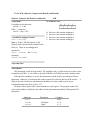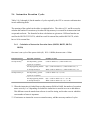
1
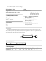
H8/500 Series
Programming Manual
Catalog No. ADE-602-021
Preface
The H8/500 Family of Hitachi-original microcontrollers is built around a 16-bit CPU core
that offers enhanced speed and a large address space. The CPU has a highly orthogonal
general-register architecture and an optimized instruction set that efficiently executes
programs coded in C language.
This manual describes the H8/500 instructions in detail, and is written for use with all chips
in the H8/500 Family. For information on assembly-language coding, see the H8/500
Series Cross Assembler User's Manual .
For details on chip hardware, see the hardware manual for the particular chip.
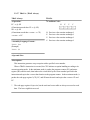
1
Section 1 CPU
1.1
Overview
The H8/500 CPU is a high-speed central processing unit designed for realtime control. It can
be used as a CPU core in application-specific integrated circuits. Its Hitachi-original
architecture features eight 16-bit general registers, internal 16-bit data paths, and an optimized
instruction set.
Section 1 summarizes the CPU architecture and instruction set.
1.1.1 Features
The main features of the H8/500 CPU are listed below.
•
•
•
•
•
*
General-register machine
— Eight 16-bit general registers
— Seven control registers (two 16-bit registers, five 8-bit registers)
High speed: maximum 10MHz
At 10MHz a register-register add operation takes only 200ns.
Address space managed in 64K-byte pages, expandable to 16M bytes*
Simultaneous control is provided of four pages: a code page, stack page, data page, and
extended page. Two address-space modes can be selected:
— Minimum mode: Maximum 64K-byte address space
— Maximum mode: Maximum 16M-byte address space*
Highly orthogonal instruction set
Addressing modes and data sizes can be specified independently within each instruction.
Optimized for efficient programming in C language
In addition to the general registers and orthogonal instruction set, the H8/500 CPU has
short two-byte formats for frequently-used instructions and addressing modes.
The CPU architecture supports up to 16M bytes, but for specific chips the maximum
address space is restricted by the number of external address lines (example: maximum
1M byte for the H8/532).
1
1.1.2 Data Structures
The H8/500 can process 1-bit data, 4-bit BCD data, 8-bit (byte) data, 16-bit (word) data, and
32-bit (longword) data.
Bit manipulation instructions operate on 1-bit data. Decimal arithmetic instructions operate on
4-bit BCD data. Almost all data transfer, shift, arithmetic, and logical operation instructions
operate on byte and word data. Multiply and divide instructions operate on longword data.
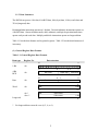
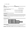
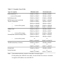
Table 1-1 lists the data formats used in general registers. Table 1-2 lists the data formats used
in memory.
(1) General Register Data Formats
Table 1-1 General Register Data Formats
Data type
Register No.
Data structure
15
1-Bit
4-Bit
BCD
Rn
0
15 14 13 12 11 10 9 8
7
15
7
Rn
8
Don't care
15
Byte
Rn
7
MSB
15
Word
Rn
Longword
*
4 3
4
3
2
1
0
0
Lower digit
0
LSB
0
MSB
LSB
31
Rn *
5
Upper digit
8
Don't care
6
16
MSB
Upper word
Rn+1 *
Lower word
15
For longword data n must be even (0, 2, 4, or 6).
2
LSB
0
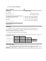
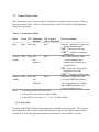
(2) Data Formats in Memory
Access to word data in memory must always begin at an even address. Access to word data
starting at an odd address causes an address error.
Table 1-2 Data Formats in Memory
Data type
Data format
1-Bit
(in byte operand)
1-Bit
(in word operand)
Byte
Word
Address n
Even address
Odd address
0
7
7
1
0
15 14 13 12 11 10 9
8
7
6
6
Address n
MSB
Even address
MSB
5
5
4
4
3
3
2
2
0
LSB
Upper 8 bits
Odd address
Lower 8 bits
Byte in
stack
Even address
Undefined data
Odd address
MSB
Word in
stack
Even address
MSB
Odd address
1
LSB
LSB
Upper 8 bits
Lower 8 bits
LSB
Note: When the stack is accessed in exception processing, word access is always performed,
regardless of the actual data size. Similarly, when the stack is accessed by an
instruction using the @–R7 or @R7+ addressing mode, word access is performed
regardless of the operand size specified in the instruction. An address error will
therefore occur if the stack pointer indicates an odd address. Programs should be
constructed so that the stack pointer always indicates an even address.
3
4
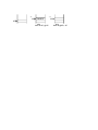
1.1.3 Address Space
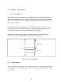
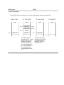
The CPU has two modes: a minimum mode which supports an address space of up to 64K
bytes, and a maximum mode which supports an address space of up to 16M bytes.
The mode is selected by input to the chip's mode pins. For details, see the H8 Hardware
Manual.
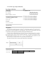
Minimum mode
Supports program and data
regions totaling up to 64K bytes.
Maximum mode
Supports program and data
regions totaling up to 16M bytes.
CPU operating mode
(1) Minimum Mode: Supports a maximum 64K-byte address space. The page register is
ignored. Branching instructions that cross page boundaries (PJMP, PJSR, PRTS, and
PRTD) are invalid.
(2) Maximum Mode: The page register is valid, supporting an address space of up to 16M
bytes. The address space is not continuous, but is divided into 64K-byte pages. When a
program crosses a page boundary, it must therefore use a page-crossing branching instruction
or an interrupt. (It is recommended for a program to be contained in a single page.) When
data access crosses a page boundary, the program must rewrite the page register before
accessing the data.
5
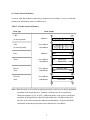
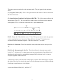
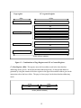
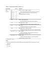
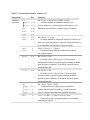
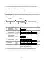
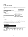
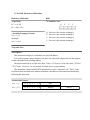
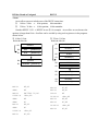
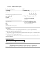
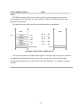
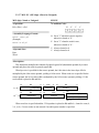
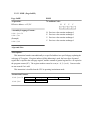
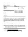
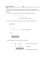
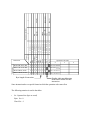
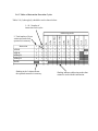
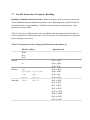
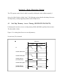
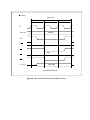
1.1.4 Register Configuration
Figure 1-2 shows the register structure of the CPU. There are two groups of registers: the
general registers (Rn) and the control registers (CR).
General registers (Rn)
15
0
R0
R1
R2
R3
R4
R5
R6 (FP)
FP: Frame Pointer
R7 (SP)
SP: Stack Pointer
Control registers (CR)
15
0
PC
PC: Program Counter
SR
CCR
15
8
T – – – – I2 I1 I 0
7
0
V
– – – – N Z
C
SR: Status Register
CCR: Condition Code Register
CP
CP: Code Page register
DP
DP: Data Page register
EP
EP: Extended Page register
TP
TP: Stack Page register
BR
BR: Base Register
6
Figure 1-1 Registers in the CPU
7
1.2
Register Descriptions
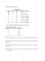
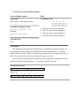
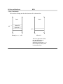
1.2.1 General Registers
All eight of the 16-bit general registers are functionally alike; there is no distinction between
data registers and address registers. When these registers are accessed as data registers, either
byte or word size can be selected. R6 and R7, in addition to functioning as general registers,
have special assignments.
R7 is the stack pointer, used implicitly in exception handling and subroutine calls. It is also
used implicitly by the LDM and STM instructions, which load and store multiple registers
from/to the stack and pre-decrement or post-increment R7 accordingly.
R6 functions as a frame pointer. High-level language compilers use R6 when they use
instructions such as LINK and UNLK to reserve or release a stack frame.
Unused area
SP →
Stack area
Figure 1-2 Stack Pointer (SP)
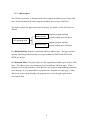
1.2.2 Control Registers
The control registers (CR) include a 16-bit program counter (PC), a 16-bit status register (SR)
containing an 8-bit condition code register (CCR), four 8-bit page registers, and one 8-bit base
register (BR).
8
The page registers are used only in the maximum mode. They are ignored in the minimum
mode.
(1) Program Counter (PC): This 16-bit register indicates the address of the next instruction
the CPU will execute.
(2) Status Register/Condition Code Register (SR/CCR): This 16-bit register indicates the
internal state of the CPU. The lower half of the status register is referred to as the condition
code register (CCR): its 8 bits can be accessed as a 1-byte condition code.
SR
CCR
15 14 13 12 11 10 9 8
T
–
–
– –
7
6
5
4 3
2
1
0
I 2 I1 I 0 –
–
–
– N Z V C
Bit 15—Trace (T): When this bit is set to "1," the CPU operates in trace mode and generates
a trace exception after every instruction. When this bit is cleared to "0" instructions are
executed in normal continuous sequence. This bit is cleared to "0" at a reset.
Bits 14 to 11—Reserved: These bits cannot be written, and when read, are always read as
"0."
Bits 10 to 8—Interrupt mask (I2 to I0): These bits indicate the interrupt request mask
level (0 to 7). As shown in 3, an interrupt request is not accepted unless it has a higher level
than the value of the mask. A nonmaskable interrupt (NMI), which has level 8, is always
accepted, regardless of the mask level.
4 indicates the values of the I bits after an interrupt is accepted. When an interrupt is accepted,
the value of bits I2 to I0 is raised to the same level as the interrupt, to prevent a further interrupt
from being accepted unless its level is higher.
A reset sets all three of bits (I2, I1, and I0) to "1."
9
Table 1-3 Interrupt Mask Levels
Priority
Interrupt mask
Level
I2 I1 I 0
Interrupts accepted
High
7
111
NMI
Low
6
5
4
3
2
1
0
110
101
100
011
010
001
000
Level 7 and NMI
Levels 6 to 7 and NMI
Levels 5 to 7 and NMI
Levels 4 to 7 and NMI
Levels 3 to 7 and NMI
Levels 2 to 7 and NMI
Levels 1 to 7 and NMI
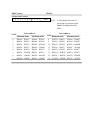
Table 1-4 Interrupt Mask Bits after an Interrupt is Accepted
Level of interrupt accepted
NMI (8)
7
6
5
4
3
2
1
I 2 I1 I0
1
1
1
1
1
0
0
0
1
1
1
0
0
1
1
0
1
1
0
1
0
1
0
1
Bits 7 to 4—Reserved: These bits cannot be written, and when read, are always read as "0."
Bit 3—Negative (N): This bit indicates the most significant bit (sign bit) of the result of an
instruction.
Bit 2—Zero (Z): This bit is set to "1" to indicate a zero result and cleared to "0" to indicate a
nonzero result.
Bit 1—Overflow (V): This bit is set to "1" when an arithmetic overflow occurs, and cleared
to "0" at other times.
10
Bit 0—Carry (C): This bit is set to "1" when a carry or borrow occurs at the most
significant bit, and is cleared to "0" (or left unchanged) at other times.
The specific changes that occur in the condition code bits when each instruction is executed are
detailed in the instruction descriptions in Section 2.2.1 and listed in Tables 2-7 (1) to (4) in
Section 2.5, "Condition Code Changes."
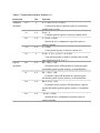
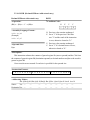
(3) Code Page Register (CP): The code page register and the program counter combine to
generate a 24-bit program code address, thereby expanding the program area. The code page
register contains the upper 8 bits of the 24-bit address.
In the maximum mode, both the code page register and program counter are saved and
restored in exception handling, and a new code page value is loaded from the exception vector
table.
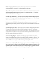
(4) Data Page Register (DP): The data page register combines with general registers R0 to
R3 to generate a 24-bit effective address, thereby expanding the data area. The data page
register contains the upper 8 bits of the 24-bit effective address. The data page register is used
to calculate effective addresses in the register indirect addressing mode using R0 to R3, and in
the 16-bit absolute addressing mode (@aa:16).
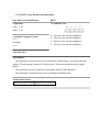
(5) Extended Page Register (EP): The extended page register combines with general
register R4 or R5 to generate a 24-bit effective address, thereby expanding the data area. The
extended page register contains the upper 8 bits of the 24-bit address. It is used to calculate
effective addresses in the register indirect addressing mode using R4 or R5.
(6) Stack Page Register (TP): The stack page register combines with R6 (Frame pointer)
or R7 (Stack pointer) to generate a 24-bit stack address, thereby expanding the stack area. The
stack page register contains the upper 8 bits of the 24-bit stack address. It is used to calculate
effective addresses in the register indirect addressing mode using R6 or R7.
11
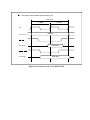
Page register
PC or general register
8 Bits
16 Bits
CP
PC
R0
R1
R2
DP
R3
@aa:16
R4
EP
R5
R6
TP
R7
24 Bits (effective address)
Figure 1-3 Combinations of Page Registers and PC or General Registers
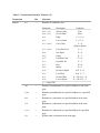
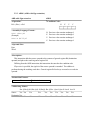
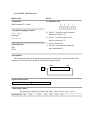
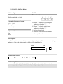
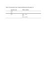
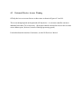
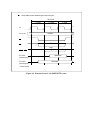
(7) Base Register (BR): This register stores the base address used in the short absolute
addressing mode (@aa:8). In the short absolute addressing mode a 16-bit operand address is
generated by using the contents of the base register as the upper 8 bits and the address given in the
instruction code as the lower 8 bits. The page is always page 0 in the short absolute addressing
mode.
8 Bits
8 Bits
BR
@aa:8
16 Bits (effective address)
12
Figure 1-4 Base Register
13
1.2.3 Initial Register Values
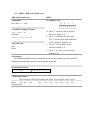
When the CPU is reset, its internal registers are initialized as shown in Table 1-5.
Table 1-5 Initial Values of CPU Registers
Initial value
Minimum mode
Maximum mode
Register
General registers
15
0
R0 – R7
Undetermined
Undetermined
Loaded from
vector table
Loaded from
vector table
H'070 * (N,
Z,V and C are
undetermined)
Undetermined
H'070 * (N,
Z,V and C are
undetermined)
Loaded from
vector table
Undetermined
Undetermined
Undetermined
Undetermined
Undetermined
Undetermined
Undetermined
Undetermined
Control registers
15
0
PC
SR
CCR
15
8
7
0
V
– – – – N Z
C
7
0
T – – – – I2 I1 I 0
CP
7
0
DP
7
0
EP
7
0
TP
7
0
BR
14
1.3
Instruction Set
The main features of the CPU instruction set are:
• A general-register architecture.
• Orthogonality. Addressing modes and data sizes can be specified independently in each
instruction.
• 1.5-type addressing (register-register and register-memory operations)
• Affinity for high-level languages, particularly C.
• Short formats for frequently-used instructions and addressing modes.
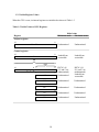
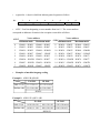
1.3.1 Types of Instructions
The CPU instruction set includes 63 types of instructions, listed by function in Table 1-6. Detailed
descriptions are given starting in Section 2.2.1.
Table 1-6 Instruction Classification
FunctionInstructions
Types
Data transfer
MOV, LDM, STM, XCH, SWAP, MOVTPE, MOVFPE
Arithmetic operations ADD, SUB, ADDS, SUBS, ADDX, SUBX, DADD, DSUB,
MULXU, DIVXU, CMP, EXTS, EXTU, TST, NEG, CLR,
7
17
Logic operations
TAS
AND, OR, XOR, NOT
4
Shift
SHAL, SHAR, SHLL, SHLR, ROTL, ROTR, ROTXL,
8
Bit manipulation
ROTXR
BSET, BCLR, BTST, BNOT
4
Bcc*, JMP, PJMP, BSR, JSR, PJSR, RTS, PRTS,
RTD, PRTD, SCB (/F, /NE, /EQ)
11
Branch
System control
TRAPA, TRAP/VS, RTE, SLEEP, LDC, STC, ANDC,
12
ORC, XORC, NOP, LINK, UNLK
Total
*: Bcc is the generic name of the conditional branch instructions.
12
63
1.3.2 Instructions Listed by Function
Tables 1-7 (1) to (6) give a concise summary of the instructions in each functional category. The
notation used in these tables is listed below.
Operation Notation
Rd
General register (destination)
Rs
Rn
(EAd)
(EAs)
CCR
N
Z
V
C
CR
PC
CP
SP
FP
#IMM
disp
+
–
×
General register (source)
General register
Destination operand
Source operand
Condition code register
N (negative) bit of CCR
Z (zero) bit of CCR
V (overflow) bit of CCR
C (carry) bit of CCR
Control register
Program counter
Code page register
Stack pointer
Frame pointer
Immediate data
Displacement
Addition
Subtraction
Multiplication
÷
∧
∨
⊕
→
↔
Division
AND logical
OR logical
Exclusive OR logical
Move
Exchange
¬
Not
Table 1-7 Instructions Listed by Function (1)
Instruction
Data
transfer
Size *2
MOV
MOV:G B/W
MOV:E
B
MOV:I
W
MOV:F B/W
MOV:L B/W
Function
(EAs) → (EAd), #IMM → (EAd)
Moves data between two general registers, or between
a general register and memory, or moves immediate
data
to a general register or memory.
MOV:S B/W
LDM
STM
XCH
SWAP
MOVTPE*1
MOVFPE*1
W
Stack → Rn (register list)
W
Pops data from the stack to one or more registers.
Rn (register list) → stack
W
Pushes data from one or more registers onto the stack.
Rs ↔ Rd
B
Exchanges data between two general registers.
Rd (upper byte) ↔ Rd (lower byte)
B
Exchanges the upper and lower bytes in a general register.
Rn → (EAd)
B
Transfers data from a general register to memory in
synchronization with the E clock.
(EAs) → Rd
Transfers data from memory to a general register in
synchronization with the E clock.
*: B—byte; W—word
Notes:
*1 Do not use the MOVTPE and MOVFPE instructions with the H8/520, which has no E-clock
output pin.
*2 B: byte
W: word
Table 1-7 Instructions Listed by Function (2)
Instruction
Size
Arithmetic
ADD
operations
ADD:G B/W
ADD:Q B/W
Function
Rd ± (EAs) → Rd, (EAd) ± #IMM → (EAd)
Performs addition or subtraction on data in two
general registers or a general register and memory, or on
SUB
B/W
immediate data and data in a general register or memory.
ADDS
SUBS
ADDX
B/W
B/W
B/W
Rd ± (EAs) ± C → Rd
SUBX
B/W
DADD
B
DSUB
B
MULXU
B/W
DIVXU
B/W
Performs addition or subtraction with carry or borrow on
data in two general registers or a general register and memory,
or on immediate data and data in a general register .
(Rd)10 ± (Rs)10 ± C → (Rd)10
Performs decimal addition or subtraction on data in
two general registers.
Rd × (EAs) → Rd
Performs 8-bit × 8-bit or 16-bit × 16-bit unsigned
multiplication on data in a general register and data in another
general register or memory, or on data in a general register
and immediate data.
Rd ÷ (EAs) → Rd
Performs 16-bit ÷ 8-bit or 32-bit ÷ 16-bit unsigned
division on data in a general register and data in another
general register or memory, or on data in a general register
and immediate data.
CMP
CMP:G B/W
CMP:E
B
CMP:I
W
Rd – (EAs), (EAd) – #IMM
Compares data in a general register with data in
another general register or memory, or with immediate
data, or compares immediate data with data in memory.
EXTS
(<bit 7> of <Rd>) → (<bits 15 to 8> of <Rd>)
B
Converts byte data in a general register to word data by
extending the sign bit.
Table 1-7 Instructions Listed by Function (3)
Instruction
Arithmetic
EXTU
Size
B
operations
Converts byte data in a general register to word data by
padding with zero bits.
TST
NEG
CLR
TAS
Logical
Function
0 → (<bits 15 to 8> of <Rd>)
AND
B/W
(EAd) – 0
B/W
Compares general register or memory contents with 0.
0 – (EAd) → (EAd)
B/W
Obtains the two's complement of general register or
memory contents.
0 → (EAd)
B
B/W
Tests general register or memory contents, then sets the
most significant bit (bit 7) to "1."
Rd ∧ (EAs) → Rd
B/W
Performs a logical AND operation on a general register
and another general register, memory, or immediate data.
Rd ∨ (EAs) → Rd
B/W
Performs a logical OR operation on a general register
and another general register, memory, or immediate data.
Rd ⊕ (EAs) → Rd
B/W
Performs a logical exclusive OR operation on a general
register and another general register, memory, or immediate
data.
¬(EAd) → (EAd)
operations
OR
XOR
NOT
Clears general register or memory contents to 0.
(EAd) – 0, (1)2 → (<bit 7> of <EAd>)
Obtains the one's complement of general register or
memory contents.
Table 1-7 Instructions Listed by Function (4)
Instruction
Shift
operations
SHAL
Size
B/W
Function
(EAd) shift → (EAd)
SHAR
B/W
SHLL
B/W
Performs an arithmetic shift operation on general register
or memory contents.
(EAd) shift → (EAd)
SHLR
B/W
ROTL
B/W
Performs a logical shift operation on general register or
memory contents.
(EAd) rotate → (EAd)
ROTR
ROTXL
B/W
B/W
Rotates general register or memory contents.
(EAd) rotate with carry → (EAd)
ROTXR
B/W
Rotates general register or memory contents through the C
(carry) bit.
¬(<bit-No.> of <EAd>) → Z,
1 → (<bit-No.> of <EAd>)
Bit
BSET
manipulations
BCLR
B/W
B/W
Tests a specified bit in a general register or memory, then
sets the bit to "1." The bit is specified by a bit-number given
in immediate data or a general register.
¬(<bit-No.> of <EAd>) → Z,
0 → (<bit-No.> of <EAd>)
BNOT
B/W
Tests a specified bit in a general register or memory, then
clears the bit to "0." The bit is specified by a bit-number
given in immediate data or a general register.
¬(<bit-No.> of <EAd>) → Z,
→ (<bit-No.> of <EAd>)
BTST
B/W
Tests a specified bit in a general register or memory, then
inverts the bit. The bit is specified by a bit-number given in
immediate data or a general register.
¬(<bit-No.> of <EAd>) → Z,
Tests a specified bit in a general register or memory. The
bit is specified by a bit-number given in immediate data or a
general register.
Table 1-7 Instructions Listed by Function (5)
Instruction
Branch
Size
Bcc
—
Function
Branches if condition is true.
Mnemonic
Description
Condition
BRA (BT)
Always (true)
True
BRN (BF)
BHI
BLS
Never (false)
High
Low or Same
False
C∨Z=0
C∨Z=1
BCC (BHS)
Carry Clear
BCS (BLO)
BNE
BEQ
BVC
BVS
BPL
BMI
BGE
BLT
BGT
BLE
Carry Set (Low)
Not Equal
Equal
Overflow Clear
Overflow Set
Plus
Minus
Greater or Equal
Less Than
Greater Than
Less or Equal
C=0
(High or Same)
C=1
Z=0
Z=1
V=0
V=1
N=0
N=1
N⊕V=0
N⊕V=1
Z ∨ (N ⊕ V) = 0
Z ∨ (N ⊕ V) = 1
(∨ = Logic OR)
JMP
—
PJMP
—
BSR
—
JSR
—
PJSR
—
RTS
—
Branches unconditionally to a specified address in the same
page.
Branches unconditionally to a specified address in a specified
page.
Branches to a subroutine at a specified address in the same
page.
Branches to a subroutine at a specified address in the same
page.
Branches to a subroutine at a specified address in a specified
page.
Returns from a subroutine in the same page.
Table 1-7 Instructions Listed by Function (6)
Instruction
Branch
System
control
PRTS
RTD
Size
—
—
PRTD
—
SCB/F
SCB/NE
SCB/EQ
TRAPA
—
—
—
—
Function
Returns from a subroutine in a different page.
Returns from a subroutine in the same page and adjusts
the stack pointer.
Returns from a subroutine in a different page and adjusts
the stack pointer.
Controls a loop using a loop counter and/or a specified.
CCR termination condition.
Generates a trap exception with a specified vector
number.
TRAP/VS —
Generates a trap exception if the V bit is set when the
instruction is executed.
RTE
—
Returns from an exception-handling routine.
LINK
—
FP → @–SP; SP → FP; SP + #IMM → SP
Creates a stack frame.
UNLK
—
FP → SP; @SP+ → FP
Deallocates a stack frame created by the LINK
instruction.
SLEEP
—
Causes a transition to the power-down state.
LDC
B/W*
(EAs) → CR
Moves immediate data or general register or memory
contents to a specified control register.
STC
B/W*
CR → (EAd)
Moves control register data to a specified general register
or memory location.
ANDC
B/W*
CR ∧ #IMM → CR
Logically ANDs a control register with immediate data.
ORC
B/W*
CR ∨ #IMM → CR
Logically ORs a control register with immediate data.
XORC
B/W*
CR ⊕ #IMM → CR
Logically exclusive-ORs a control register with immediate
data.
NOP
—
PC + 1 → PC
No operation. Only increments the program counter.
* The size depends on the control register.
1.3.3 Short Format Instructions
The ADD, CMP, and MOV instructions have special short formats. Table 1-8 lists these short
formats together with the equivalent general formats.
The short formats are a byte shorter than the corresponding general formats, and most of them
execute one state faster.
Table 1-8 Short-Format Instructions and Equivalent General Formats
Short-format
instruction
ADD:Q
CMP:E
CMP:I
MOV:E
MOV:I
MOV:L
MOV:S
MOV:F
MOV:F
Execution Equivalent generalLength states *2
format instruction
#xx,Rd *1
#xx:8,Rd
#xx:16,Rd
#xx:8,Rd
#xx:16,Rd
@aa:8,Rd
Rs,@aa:8
@(d:8,R6),Rd
Rs,@(d:8,R6)
2
2
3
2
3
2
2
2
2
2
2
3
2
3
5
5
5
5
Length
ADD:G #xx:8,Rd
CMP:G.B #xx:8,Rd
CMP:G.W #xx:16,Rd
MOV:G.B #xx:8,Rd
MOV:G.W #xx:16,Rd
MOV:G @aa:8,Rd
MOV:G Rs,@aa:8
MOV:G @(d:8,R6),Rd
MOV:G Rs,@(d:8,R6)
Execution
states *2
3
3
4
3
4
3
3
3
3
3
3
4
3
4
5
5
5
5
Notes:
*1 The ADD:Q instruction accepts other destination operands in addition to a general register, but
the immediate data value (#xx) is limited to ±1 or ±2.
*2 Number of execution states for access to on-chip memory. For the H8/510, the number of
execution states for general register access.
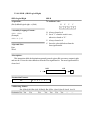
1.3.4 Basic Instruction Formats
There are two basic CPU instruction formats: the general format and the special format.
(1) General format: This format consists of an effective address (EA) field, an effective address
extension field, and an operation code (OP) field. It is used in arithmetic instructions and other
general instructions.
• Effective address field:
One byte containing information used to calculate the effective
address of an operand.
• Effective address extension:
Zero to two bytes containing a displacement value, immediate data,
or an absolute address.
• Operation code:
Defines the operation to be carried out on the operand located at the
address calculated from the effective address information. Each
instruction has a unique operation code.
Fetch direction
Effective address
Effective address extension
Operation code
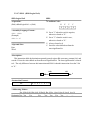
Note: Some instructions (DADD, DSUB, MOVFPE, MOVTPE) have an extended format in which
the operand code is preceded by a one-byte prefix code.
(Example: MOVTPE instruction)
Prefix code
Effective address
0 0
0
0
0
0
Operation code
0
0 1
0
0
1 0
r
r
r
r r r: General register No.
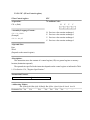
(2) Special format: In this format the operation code comes first, followed by the effective
address field and effective address extension. This format is used in branching instructions, system
control instructions, and other instructions that can be executed faster if the operation to be
performed on the operand is specified first.
•
Operation code:
One or two bytes defining the operation to be performed by the instruction.
•
Effective address field and effective address extension: Zero to three bytes containing
information used to calculate the effective address of an operand.
Fetch direction
Operation code
Effective address
Effective address extension
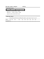
1.3.5 Addressing Modes and Effective Address Calculation
The CPU supports the seven addressing modes listed in Table 1-9 below. Due to the highly
orthogonal nature of the instruction set, most instructions having operands can use any applicable
addressing mode from 1 through 6. Mode 7 is used by branching instructions.
Table 1-9 explains how the effective address (EA) is calculated in each addressing mode.
Table 1-9 Addressing Modes
No. Addressing mode
Mnemonic Effective Address and Extension
Bytes
1
1
1
Register direct
Rn
1 0 1 0 Sz r r r *1, *2
2
Register indirect
@Rn
1 1 0 1 Sz r r r
3
Register indirect
with displacement
@(d:8,Rn) 1 1 1 0 Sz r r r
@(d:16,Rn) 1 1 1 1 Sz r r r
4
5
6
7
disp
disp (H)
disp (L)
2
3
Register indirect
@–Rn
with pre-decrement
Register indirect
@Rn+
with post-increment
1 0 1 1 Sz r r r
1
1 1 0 0 Sz r r r
1
Absolute address *3 @aa:8
@aa:16
0 0 0 0 Sz 1 0 1
addr (L)
0 0 0 1 Sz 1 0 1
addr (H)
Immediate
#xx:8
#xx:16
00000 100
data
00001 100
data (H)
disp
Effective address information is
specified in the operation code.
PC-relative
addr (L)
2
3
data (L)
2
3
otes:
*1 Sz: Operand size
Sz = 0: byte operand
Sz = 1: word operand
*2 rrr (register number field): General register number
000: R0
001: R1
010: R2
011: R3
100: R4
101: R5
110: R6
111: R7
*3 The @aa:8 addressing mode may be referred to as the short absolute addressing mode.
1 or 2
N
Table 1-10 Effective Address Calculation (1)
No. Addressing mode
1 Register direct
Effective address
calculation
None
Effective address
Operand is contents of Rn.
Rn
1 0 1 0 Sz r r r
2
Register indirect
None
23
15
*1
DP/TP/EP
@Rn
1 1 0 1 Sz r r r
3
0
Rn
*2
Register indirect
with displacement
@(d:8,Rn)
1 1 1 0 Sz r r r
8 bit
15
Rn contents
15
disp (sign extention)
∨
⊕
∧
23
15
*1
DP/TP/EP
0
Result
Ÿ
*2
--------------------------------------------------------------@(d:16,Rn)
16 bit
1 1 1 1 Sz r r r
15
Rn contents
15
disp
4
➀ Register indirect
with pre-decrement
15
@–Rn
15
1 0 1 1 Sz r r r
➁ Register indirect
with post-increment
Rn contents
1 or 2
∨
⊕
∧
∨
_
∧
23
15
DP/TP/EP *1
*2
23
15
DP/TP/EP *1
5
Absolute address
@aa:8
0
Result
Ÿ
*2
Rn is decremented by –1 or –2 before instruction execution. *3, *4, *5
None
23
15
DP/TP/EP *1
0
Rn
*2
@Rn+
1 1 0 0 Sz r r r
0
Result
Ÿ
Rn is incremented by +1 or +2 after instruction execution. *3, *4, *5
None
23
15
H'00
0
BR
↵
EA extension data
0 0 0 1 Sz 1 0 1
--------------------------------------------------------------@aa:16
None
23
15
0
0 0 0 0 Sz 1 0 1
DP *1
EA extension data
Table 1-10 Effective Address Calculation (2)
No. Addressing mode
6
Immediate
#xx:8
Effective address
calculation
Effective address
None
Operand is 1-byte
EA extension data.
00000100
--------------------------------------------------------------#xx:16
Operand is 2-byte
None
00001100
EA extension data
7
PC-relative
d:8
8 Bits
15
23
PC
15
15
CP *1
∨
⊕
∧
0
Result
Ÿ
↑
Displacement (sign extension)
--------------------------------------------------------------d:16
16 Bits
15
23
PC
15
disp
∨
⊕
∧
15
CP *1
0
Result
Ÿ
Notes:
1. The page register is ignored in the minimum mode.
2. In addressing modes No. 2, 3, and 4, the page register is as follows:
DP for register-indirect addressing with R0, R1, R2, or R3.
EP for register-indirect addressing with R4 or R5.
TP for register indirect addressing with R6 or R7.
3. Increment (Decrement) by 1 for a byte operand, and by 2 for a word operand.
4. In addressing mode No. 4 (register indirect with pre-decrement or post-increment), when register
R7 is specified the increment or decrement is always ±2, even when operand size is 1 byte.
5. If SP is saved by @-SP addressing mode and poped by @SP+, the result will be as follows.
→
SP
Old SP-2
→
SP
SP
after
MOV.W SP, @-SP
after
MOV.W @SP+, SP
1.3.6 Register Specification
(1) General Register Specification: General registers are specified by a three-bit register
number contained in the instruction code. Another bit may be used to indicate whether a
register operand is a byte or word operand. See Table 1-11.
Table 1-11 General Register Specification
EA:
OP:
Sz:
r i r i ri / r j r j r j:
EA field
OP field
* * * * Sz ri ri ri * * * * * rj rj rj
ri ri ri / rj rj rj
Sz = 0 (Byte)
15
000
001
010
011
100
101
110
111
Effective address
Operation code
Size (byte/word)
General register number
Sz = 1 (Word)
8 7
0
15
0
Not used
R0
R0
Not used
R1
R1
Not used
R2
R2
Not used
R3
R3
Not used
R4
R4
Not used
R5
R5
Not used
R6
R6
Not used
R7
R7
25
(2) Control Register Specification: Control registers are specified by a control register
number embedded in the operation code byte. See Table 1-12.
Table 1-12 Control Register Specification
EA field
Effective address
ccc
000
OP field
Sz = 0 (Byte)
111
Sz = 1 (Word)
(Not allowed*)
7
001
010
011
100
101
110
c c c: Control register number field
* * * * * ccc
0
CCR
(Not allowed)
BR
EP
DP
(Not allowed)
TP
15
0
SR
(Not allowed)
(Not allowed)
(Not allowed)
(Not allowed)
(Not allowed)
(Not allowed)
(Not allowed)
*
Control register numbers indicated as "(Not allowed)" should not be used, because they
may cause the CPU to malfunction.
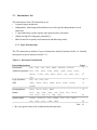
Section 2 Instruction Set: Detailed Descriptions
2.1 Table Format and Notation
Each instruction is described in a table with the following format:
Name
Mnemonic
<Operation>
<Condition Code>
<Assembly-Language Format>
<Operand Size>
<Description>
<Instruction Format>
<Addressing Modes>
Name: A name indicating the function of the instruction.
Mnemonic: The assembly-language mnemonic of the instruction.
Operation: A concise, symbolic indication of the operation performed by the instruction.
The notation used is listed on the next page.
Operation notation
Rd
General register (destination)
Rs
Rn
(EAd)
(EAs)
CCR
N
Z
V
C
CR
PC
CP
SP
General register (source)
General register
Destination operand
Source operand
Condition code register
N (negative) bit of CCR
Z (zero) bit of CCR
V (overflow) bit of CCR
C (carry) bit of CCR
Control register
Program counter
Code page register
Stack pointer
FP
#IMM
disp
+
–
×
Frame pointer
Immediate data
Displacement
Addition
Subtraction
Multiplication
÷
∧
∨
⊕
→
↔
Division
AND logical
OR logical
Exclusive OR logical
Move
Exchange
¬
Not
Condition code: Changes in the condition code (N, Z, V, C) after instruction execution are
indicated by the following symbols:
—:
*:
↕:
0:
1:
∆:
Not changed.
Undetermined
Changed according to the result of the instruction.
Always cleared to "0."
Always set to "1."
Handling depends on the operand.
Section 2.5, "Condition Code Changes," lists these changes with explicit formulas showing how the
bit values are derived.
Assembly-language format: The assembly-language coding of the instruction is indicated as
below.
(Example) ADD <EAs>, Rd
Destination operand
Source operand
Mnemonic
29
For details on assembly-language notation, see the H8/500 Series Cross Assembler Manual.
Operand size: The available operand sizes are indicated.
Description: A detailed description of the instruction.
Instruction format: The machine-language instruction format, including the effective address, is
indicated as shown below.
EA field
EA
Effective address
OP field
1
0
1
1 0
r
r
r
r r r: Register number field
Register No. c c c: Control register number field
Operation code
No. Addressing mode Mnemonic Effective address and extension
Bytes
1
Register direct
Rn
1 0 1 0 Sz r r r
1
2
Register indirect
@Rn
1 1 0 1 Sz r r r
1
3
Register indirect
with displacement
@(d:8,Rn) 1 1 1 0 Sz r r r
@(d:16,Rn) 1 1 1 1 Sz r r r
Register indirect
@–Rn
1 0 1 1 Sz r r r
1
with pre-decrement
Register indirect
@Rn+
with post-increment
1 1 0 0 Sz r r r
1
Absolute address*
@aa:8
0 0 0 0 Sz 1 0 1
addr (L)
@aa:16
0 0 0 1 Sz 1 0 1
addr (H)
#xx:8
00000100
data
#xx:16
00001100
data (H)
disp
Effective address information is
4
5
6
7
Immediate
PC-relative
disp
disp (H)
disp (L)
addr (L)
2
3
2
data (L)
specified in the operation code.
The @aa:8 addressing mode may be referred to as the short absolute addressing mode.
30
2
3
3
1 or 2
*
Addressing modes: The addressing modes that can be specified for the source and destination
operands are indicated in a table like the one below. "Yes" means that the mode can be used;
"—" means that it cannot.
(Example: ADD instruction)
Rn @Rn @(d:8,Rn) @(d:16,Rn)@–Rn @Rn+ @aa:8 @aa:16 #xx:8 #xx:16
Source
Yes Yes
Yes
Yes
Yes
Yes
Yes
Yes
Yes
Yes
DestinationYes —
—
—
—
—
—
—
—
—
Symbol
Meaning
Rn
Register direct
@Rn
@(d:8,Rn)
@(d:16,Rn)
@–Rn
@Rn+
@aa:8
@aa:16
#xx:8
#xx:16
Register indirect
Register indirect with 8-bit displacement
Register indirect with 16-bit displacement
Register indirect with pre-decrement
Register indirect with post-increment
Short absolute address (8 bits)
Absolute address (16 bits)
Immediate (8 bits)
Immediate (16 bits)
2.2
Instruction Descriptions
The individual instructions are described starting in Section 2.2.1.
31
2.2.1 ADD
(1) ADD:G (ADD, General format)
ADD Binary
ADD:G
<Operation>
Rd + (EAs) → Rd
<Condition Code>
N
↕
Z
↕
V
↕
C
↕
<Assembly-Language Format>
N: Set to "1" when the result is negative;
otherwise cleared to "0."
Z: Set to "1" when the result is zero;
otherwise cleared to "0."
V: Set to "1" if an overflow occurs;
otherwise cleared to "0."
C: Set to "1" if a carry occurs; otherwise
cleared to "0."
ADD:G <EAs>,Rd
(Example)
(1)
(2)
ADD:G.B R0,R1
ADD.B R0,R1*
<Operand Size>
Byte
Word
<Description>
This instruction adds the source operand to the contents of general register Rd (destination
operand) and places the result in general register Rd.
When the source operand is the immediate data ±1 or ±2, the ADD:Q instruction in Section 2.2.1
(2) can be used. The ADD:Q instruction is shorter and executes more quickly.
<Instruction Format>
EA
0
0
1
0 0
r
r
r
<Addressing Modes>
Rn @Rn @(d:8,Rn) @(d:16,Rn)@–Rn @Rn+ @aa:8 @aa:16 #xx:8 #xx:16
Source
Yes Yes
Yes
Yes
Yes
Yes
Yes
Yes
Yes
Yes
DestinationYes —
—
—
—
—
—
—
—
—
32
* In assembly-language coding it is usually not necessary to specify the general or special format
(by coding :G etc.). If the format specification is omitted, the assembler automatically generates
the optimum object code. If a format is specified, the assembler follows the format specification.
2.2.1 (2) ADD:Q (ADD Quick, short format)
ADD Quick
ADD:Q
<Operation>
(EAd) + #IMM → (EAd)
<Condition Code>
N
↕
Z
↕
V
↕
C
↕
<Assembly-Language Format>
N: Set to "1" when the result is negative;
otherwise cleared to "0."
Z: Set to "1" when the result is zero;
otherwise cleared to "0."
V: Set to "1" if an overflow occurs;
otherwise cleared to "0."
C: Set to "1" if a carry occurs; otherwise
cleared to "0."
ADD:Q #xx, <EAd>
(Example)
(1)
(2)
ADD:Q.W #1,@R0
ADD.W #1,@R0*
<Operand Size>
Byte
Word
<Description>
This instruction adds immediate data to the destination operand and places the result in the
destination operand.
The values ±1 and ±2 can be specified as immediate data.
<Instruction Format>
ADD:Q #1,<EAd>
EA
0
0
0
0 1
0
0
0
ADD:Q #2,<EAd>
EA
0
0
0
0 1
0
0
1
ADD:Q #–1,<EAd>
EA
0
0
0
0 1
1
0
0
ADD:Q #–2,<EAd>
EA
0
0
0
0 1
1
0
1
<Addressing Modes>
Rn @Rn @(d:8,Rn) @(d:16,Rn)@–Rn @Rn+ @aa:8 @aa:16 #xx:8 #xx:16
DestinationYes Yes
Yes
Yes
Yes
Yes
Yes
Yes
—
—
* In assembly-language coding it is usually not necessary to specify the general or special format
(by coding :G etc.). If the format specification is omitted, the assembler automatically generates
the optimum object code. If a format is specified, the assembler follows the format specification.
2.2.2 ADDS (ADD with Sign extension)
ADD with Sign extension
ADDS
<Operation>
Rd + (EAs) → Rd
<Condition Code>
N
—
Z
—
V
—
C
—
<Assembly-Language Format>
N:
Z:
V:
C:
ADDS <EAs>,Rd
(Example)
ADDS.W #H'10,R3
Previous value remains unchanged.
Previous value remains unchanged.
Previous value remains unchanged.
Previous value remains unchanged.
<Operand Size>
Byte
Word
<Description>
This instruction adds the source operand to the contents of general register Rd (destination
operand) and places the result in general register Rd.
Differing from the ADD instruction, this instruction does not alter the condition code.
If byte size is specified, the sign bit of the source operand is extended. The addition is
performed using the resulting word data. General register Rd is always accessed as a word-size
operand.
<Instruction Format>
EA
0
0
1
0 1
r
r
r
<Addressing Modes>
Rn @Rn @(d:8,Rn) @(d:16,Rn)@–Rn @Rn+ @aa:8 @aa:16 #xx:8 #xx:16
Source
Yes Yes
Yes
Yes
Yes
Yes
Yes
Yes
Yes
Yes
DestinationYes —
—
—
—
—
—
—
—
—
2.2.3 ADDX (ADD with eXtend carry)
ADD with eXtend carry
ADDX
<Operation>
Rd + (EAs) + C → Rd
<Condition Code>
N
Z
V
C
↕
↕
↕
↕
<Assembly-Language Format>
N: Set to "1" when the result is negative;
otherwise cleared to "0."
Z: Set to "1" if the previous Z bit value
was "1" and the result of the instruction
is zero; otherwise cleared to "0."
V: Set to "1" if an overflow occurs;
otherwise cleared to "0."
C: Set to "1" if a carry occurs; otherwise
cleared to "0."
ADDX <EAs>, Rd
(Example)
ADDX.B @(H'20,R4),R0
<Operand Size>
Byte
Word
<Description>
This instruction adds the source operand and the C bit to the contents of general register Rd
(destination operand) and places the result in general register Rd.
<Instruction Format>
EA
1
0
1
0 0
r
r
r
<Addressing Modes>
Rn @Rn @(d:8,Rn) @(d:16,Rn)@–Rn @Rn+ @aa:8 @aa:16 #xx:8 #xx:16
Source
Yes Yes
Yes
Yes
Yes
Yes
Yes
Yes
Yes
Yes
DestinationYes —
—
—
—
—
—
—
—
—
2.2.4 AND (AND logical)
AND logical
AND
<Operation>
Rd ∧ (EAs) → Rd
<Condition Code>
N
Z
V
C
↕
↕
0
—
<Assembly-Language Format>
N: Set to "1" when the MSB of the result
is "1;" otherwise cleared to "0."
Z: Set to "1" when the result is zero;
otherwise cleared to "0."
V: Always cleared to 0.
C: Previous value remains unchanged.
AND <EAs>,Rd
(Example)
AND.B @H'F8:8,R1
<Operand Size>
Byte
Word
<Description>
This instruction obtains the logical AND of the source operand and the contents of general
register Rd (destination operand) and places the result in general register Rd.
<Instruction Format>
EA
0
1
0
1 0
r
r
r
<Addressing Modes>
Rn @Rn @(d:8,Rn) @(d:16,Rn)@–Rn @Rn+ @aa:8 @aa:16 #xx:8 #xx:16
Source
Yes Yes
Yes
Yes
Yes
Yes
Yes
Yes
Yes
Yes
DestinationYes —
—
—
—
—
—
—
—
—
2.2.5 ANDC (AND Control register)
AND Control register
ANDC
<Operation>
CR ∧ #IMM → CR
<Condition Code>
N
∆
Z
∆
V
∆
C
∆
<Assembly-Language Format>
(1) When CR is the status register (SR or CCR),
the N, Z, V, and C bits are set according to
the result of the operation.
(2) When CR is not the status register (EP, TP,
DP, or BR), the bits are set as below.
N: Set to "1" when the MSB of the result is "1;"
otherwise cleared to "0."
Z: Set to "1" when the result is zero; otherwise
cleared to "0."
V: Always cleared to 0.
C: Previous value remains unchanged.
ANDC #xx,CR
(Example)
ANDC.B #H'FE,CCR
<Operand Size>
Byte
Word
(Depends on the control register)
<Description>
This instruction ANDs the contents of a control register (CR) with immediate data and places the
result in the control register.
The operand size specified in the instruction depends on the control register as indicated in Table
1-12 in Section 1.3.6, "Register Specification."
Interrupts are not accepted and trace exception processing is not performed immediately after the
end of this instruction.
<Instruction Format>
ANDC #xx:8,CR 0 0 0 0 0 1 0 0
data
ANDC #xx:16,CR 0 0 0 0 1 1 0 0
data (H)
01 01 1 c c c
data (L)
01 01 1 c c c
<Addressing Modes>
Rn @Rn @(d:8,Rn) @(d:16,Rn)@–Rn @Rn+ @aa:8 @aa:16 #xx:8 #xx:16
Source
—
—
—
—
—
—
—
—
Yes
Yes
2.2.6 Bcc (Branch conditionally)
Branch conditionally
Bcc
<Operation>
If condition is true then PC + disp → PC
<Condition Code>
N
Z
V
C
—
—
—
—
else next;
<Assembly-Language Format>
Bcc disp
The mnemonic varies depending on the
specified condition. See <Mnemonic and
Condition Field> below.
(Example)
N:
Z:
V:
C:
Previous value remains unchanged.
Previous value remains unchanged.
Previous value remains unchanged.
Previous value remains unchanged.
BEQ LABEL
<Operand Size>
<Description>
If the condition specified in the condition field (cc) is true, the displacement (disp) is added to the
program counter and execution branches to the resulting address. If the condition is not true, the
next instruction is executed.
The displacement can be an 8- or 16-bit value. The corresponding relative branching distances
are –128 to +127 bytes and –32768 to +32767 bytes. However, it is not possible to branch across a
page boundary.
The PC value used in the address calculation is the address of the instruction immediately
following this instruction.
<Instruction Format>
0
0
1
0
c c
0
0
1
0EA
c c
disp
disp (H)
disp (L)
cc: Condition field
Branch conditionally
Bcc
<Mnemonic and Condition Field>
Mnemonic
cc field
Description
BRA (BT)
0000
Always (True)
True
BRN (BF)
BHI
BLS
0001
0010
0011
Never (False)
High
Low or Same
False
C∨Z=0
C∨Z=1
BCC (BHS) 0 1 0 0
BCS (BLO) 0 1 0 1
BNE
0110
BEQ
0111
BVC
1000
BVS
1001
BPL
1010
BMI
1011
BGE
1100
BLT
1101
BGT
1110
BLE
1111
Carry Clear
(High or Same)
Carry Set (Low)
Not Equal
Equal
Overflow Clear
Overflow Set
Plus
Minus
Greater or Equal
Less Than
Greater Than
Less or Equal
Condition
C=0
C=1
Z=0
Z=1
V=0
V=1
N=0
N=1
N⊕V=0
N⊕V=1
Z ∨ (N ⊕ V) = 0
Z ∨ (N ⊕ V) = 1
2.2.7 BCLR (Bit test and CLeaR)
Bit test and CLeaR
BCLR
<Operation>
¬(<bit No.> of <EAd>) → Z
0 → (<bit No.> of <EAd>)
<Condition Code>
N
Z
V
C
—
↕
—
—
<Assembly-Language Format>
N: Previous value remains unchanged.
Z: Set to "1" if the value of the bit tested
was zero. Otherwise cleared to "0."
V: Previous value remains unchanged.
C: Previous value remains unchanged.
BCLR #xx,<EAd>
BCLR Rs,<EAd>
(Example)
BCLR.B #7,@H'FF00
<Operand Size>
Byte
Word
<Description>
This instruction tests a specified bit in the destination operand, sets or clears the Z bit according
to the result, then clears the specified bit to "0."
The bit number (0 to 15) can be specified directly using immediate data, or can be placed in a
specified general register. If a general register is used, the lower 4 bits of the register specify the bit
number and the upper 12 bits are ignored.
<Instruction Format>
BCLR #xx,<EAd>
EA
1
1
0
1
Data
BCLR Rs,<EAd>
EA
0
1
0
1 1
r
r
r
<Addressing Modes>
Rn @Rn @(d:8,Rn) @(d:16,Rn)@–Rn @Rn+ @aa:8 @aa:16 #xx:8 #xx:16
DestinationYes Yes
Yes
Yes
Yes
Yes
Yes
Yes
—
—
2.2.8 BNOT (Bit test and NOT)
Bit test and NOT
BNOT
<Operation>
¬(<bit No.> of <EAd>) → Z
→ (<bit No.> of <EAd>)
<Condition Code>
N
Z
V
C
—
↕
—
—
<Assembly-Language Format>
N: Previous value remains unchanged.
Z: Set to "1" if the value of the bit tested
was zero. Otherwise cleared to "0."
V: Previous value remains unchanged.
C: Previous value remains unchanged.
BNOT #xx, <EAd>
BNOT Rs,<EAd>
(Example)
BNOT.W R0,R1
<Operand Size>
Byte
Word
<Description>
This instruction tests a specified bit in the destination operand, sets or clears the Z bit according
to the result, then inverts the specified bit.
The bit number (0 to 15) can be specified directly using immediate data, or can be placed in a
specified general register. If a general register is used, the lower 4 bits of the register specify the bit
number and the upper 12 bits are ignored.
<Instruction Format>
BNOT #xx,<EAd>
EA
1
1
1
0
Data
BNOT Rs,<EAd>
EA
0
1
1
0 1
r
r
r
<Addressing Modes>
Rn @Rn @(d:8,Rn) @(d:16,Rn)@–Rn @Rn+ @aa:8 @aa:16 #xx:8 #xx:16
DestinationYes Yes
Yes
Yes
Yes
Yes
Yes
Yes
—
—
2.2.9 BSET (Bit test and SET)
Bit test and SET
BSET
<Operation>
¬(<bit No.> of <EAd>) → Z
1 → (<bit No.> of <EAd>)
<Condition Code>
N
Z
V
C
—
↕
—
—
<Assembly-Language Format>
N: Previous value remains unchanged.
Z: Set to "1" if the value of the bit tested
was zero. Otherwise cleared to "0."
V: Previous value remains unchanged.
C: Previous value remains unchanged.
BSET #xx, <EAd>
BSET Rs, <EAd>
(Example)
BSET.B #0,@R1+
<Operand Size>
Byte
Word
<Description>
This instruction tests a specified bit in the destination operand, sets or clears the Z bit according
to the result, then sets the specified bit to "1."
The bit number (0 to 15) can be specified directly using immediate data, or can be placed in a
specified general register. If a general register is used, the lower 4 bits of the register specify the bit
number and the upper 12 bits are ignored.
<Instruction Format>
BSET #xx,<EAd>
EA
1
1
0
0
Data
BSET Rs,<EAd>
EA
0
1
0
0 1
r
r
r
<Addressing Modes>
Rn @Rn @(d:8,Rn) @(d:16,Rn)@–Rn @Rn+ @aa:8 @aa:16 #xx:8 #xx:16
DestinationYes Yes
Yes
Yes
Yes
Yes
Yes
Yes
—
—
2.2.10 BSR (Branch to SubRoutine)
Branch to SubRoutine
BSR
<Operation>
PC → @–SP
PC + disp → PC
<Condition Code>
N
Z
V
C
—
—
—
—
<Assembly-Language Format>
N:
Z:
V:
C:
BSR disp
(Example)
BSR LABEL
Previous value remains unchanged.
Previous value remains unchanged.
Previous value remains unchanged.
Previous value remains unchanged.
<Operand Size>
<Description>
This instruction branches to a subroutine at a specified address.
It saves the program counter contents to the stack area, then adds a displacement to the program
counter and jumps to the resulting address.
The displacement can be an 8-bit value from –128 to +127 bytes or 16-bit value from –32768 to
+32767 bytes. However, it is not possible to branch across a page boundary.
This instruction is paired with the RTS instruction to execute a subroutine call. The PC value
saved to the stack and used in the address calculation is the address of the instruction immediately
following this instruction.
<Instruction Format>
BSR d:8
0
0
0
0 1
1
1
0
BSR d:16 0 0 0 1 1
1
1
0
disp
disp (H)
disp (L)
2.2.11 BTST (Bit TeST)
Bit TeST
BTST
<Operation>
¬(<bit No.> of <EAd>) → Z
<Condition Code>
N
Z
V
C
—
↕
—
—
<Assembly-Language Format>
N: Previous value remains unchanged.
Z: Set to "1" if the value of the bit tested
was zero. Otherwise cleared to "0."
V: Previous value remains unchanged.
C: Previous value remains unchanged.
BTST #xx, <EAd>
BTST Rs, <EAd>
(Example)
BTST.B R0,@H'F0:8
<Operand Size>
Byte
Word
<Description>
This instruction tests a specified bit in the destination operand and sets or clears the Z bit
according to the result.
The bit number (0 to 15) can be specified directly using immediate data, or can be placed in a
specified general register. If a general register is used, the lower 4 bits of the register specify the bit
number and the upper 12 bits are ignored.
<Instruction Format>
BTST #xx,<EAd>
EA
1
1
1
1
Data
BTST Rs,<EAd>
EA
0
1
1
1 1
r
r
r
<Addressing Modes>
Rn @Rn @(d:8,Rn) @(d:16,Rn)@–Rn @Rn+ @aa:8 @aa:16 #xx:8 #xx:16
DestinationYes Yes
Yes
Yes
Yes
43
Yes
Yes
Yes
—
—
2.2.12 CLR (CLeaR)
CLeaR
CLR
<Operation>
0 → (EAd)
<Condition Code>
N
Z
V
C
0
1
0
0
<Assembly-Language Format>
N:
Z:
V:
C:
CLR <EAd>
(Example)
CLR.W @(H'1000,R5)
Always cleared to 0.
Always set to 1.
Always cleared to 0.
Always cleared to 0.
<Operand Size>
Byte
Word
<Description>
This instruction clears the destination operand (general register Rn or an operand in memory) to
zero.
<Instruction Format>
EA
0
0
0
1 0
0
1
1
<Addressing Modes>
Rn @Rn @(d:8,Rn) @(d:16,Rn)@–Rn @Rn+ @aa:8 @aa:16 #xx:8 #xx:16
DestinationYes Yes
Yes
Yes
Yes
Yes
Yes
Yes
—
—
2.2.13 CMP
(1) CMP:G (CoMPare, General format)
CoMPare
CMP:G
<Operation>
Set CCR according to result of (EAd) – #IMM
Set CCR according to result of Rd – (EAs)
<Condition Code>
N
Z
V
C
↕
↕
↕
↕
<Assembly-Language Format>
N: Set to "1" when the result is negative;
otherwise cleared to "0."
Z: Set to "1" when the result is zero;
otherwise cleared to "0."
V: Set to "1" if an overflow occurs;
otherwise cleared to "0."
C: Set to "1" if a borrow occurs;
otherwise cleared to "0."
CMP:G #xx,<EAd>
CMP:G <EAs>,Rd
(Example)
(1)
(2)
CMP:G.B #H'AA,@–R3
CMP.B #H'AA,@–R3*
<Operand Size>
Byte
Word
<Description>
This instruction subtracts the source operand from the destination operand and sets or clears the
condition code (CCR) according to the result. It does not alter the destination operand.
The CMP instruction also has short formats (CMP:E and CMP:I) that can be used to compare a
general register with immediate data.
<Instruction Format>
CMP #xx,<EAd>
CMP <EAs>,Rd
*
EA
0 0 0 0 0 1 00
data*
EA
0 0 0 0 0 1 01
data (H)*
EA
01 11 0 r r r
data (L)*
The length of the immediate data depends on the size (Sz) specified for the first operation code:
one byte when Sz = 0; one word when Sz = 1.
* In assembly-language coding it is usually not necessary to specify the general or special format
(by coding :G etc.). If the format specification is omitted, the assembler automatically generates
the optimum object code. If a format is specified, the assembler follows the format specification.
CoMPare
CMP:G
<Addressing Modes>
CMP #xx,<EAd>
Rn @Rn @(d:8,Rn) @(d:16,Rn)@–Rn @Rn+ @aa:8 @aa:16 #xx:8 #xx:16
Source
— —
Destination — Yes
—
Yes
—
Yes
—
Yes
—
Yes
—
Yes
—
Yes
Yes
—
Yes
—
CMP <EAs>,Rd
Rn @Rn @(d:8,Rn) @(d:16,Rn)@–Rn @Rn+ @aa:8 @aa:16 #xx:8 #xx:16
Source
Yes Yes
Yes
Yes
Yes
Yes
Yes
Yes
Yes
Yes
DestinationYes —
—
—
—
—
—
—
—
—
2.2.13 (2) CMP:E (CoMPare:E, short format)
CoMPare immediate bytE
CMP:E
<Operation>
Set CCR according to result of Rd – #IMM
<Condition Code>
N
Z
V
C
↕
↕
↕
↕
<Assembly-Language Format>
N: Set to "1" when the result is negative;
otherwise cleared to "0."
Z: Set to "1" when the result is zero;
otherwise cleared to "0."
V: Set to "1" if an overflow occurs;
otherwise cleared to "0."
C: Set to "1" if a borrow occurs;
otherwise cleared to "0."
CMP:E #xx:8,Rd
(Example)
(1)
(2)
CMP:E #H'00,R0
CMP.B #H'00,R0*
<Operand Size>
Byte
<Description>
This instruction subtracts one byte of immediate data from general register Rd and sets or
clears the condition code (CCR) according to the result. It does not alter the contents of
general register Rd.
This instruction is a short form of the CMP instruction. Compared with CMP:G #xx:8,
Rd, its object code is one byte shorter and it executes one state faster.
<Instruction Format>
01 00 0 r r r
data
<Addressing Modes>
Rn @Rn @(d:8,Rn) @(d:16,Rn)@–Rn @Rn+ @aa:8 @aa:16 #xx:8 #xx:16
Source
—
—
—
—
—
—
—
—
Yes
—
DestinationYes —
—
—
—
—
—
—
—
—
* In assembly-language coding it is usually not necessary to specify the general or special format
(by coding :G etc.). If the format specification is omitted, the assembler automatically generates
the optimum object code. If a format is specified, the assembler follows the format specification.
2.2.13 (3) CMP:I (CoMPare:I, short format)
CoMPare Immediate word
CMP:I
<Operation>
Set CCR according to result of Rd – #IMM
<Condition Code>
N
Z
V
C
↕
↕
↕
↕
<Assembly-Language Format>
N: Set to "1" when the result is negative;
otherwise cleared to "0."
Z: Set to "1" when the result is zero;
otherwise cleared to "0."
V: Set to "1" if an overflow occurs;
otherwise cleared to "0."
C: Set to "1" if a borrow occurs;
otherwise cleared to "0."
CMP:I #xx:16,Rd
(Example)
(1)
(2)
CMP:I #H'FFFF,R1
CMP.W #H'FFFF,R1*
<Operand Size>
Word
<Description>
This instruction subtracts one word of immediate data from general register Rd and sets or clears
the condition code (CCR) according to the result. It does not alter the contents of general register
Rd.
This instruction is a short form of the CMP instruction. Compared with CMP:G #xx:16, Rd, its
object code is one byte shorter and it executes one state faster.
<Instruction Format>
01 00 1 r r r
data (H)
data (L)
<Addressing Modes>
Rn @Rn @(d:8,Rn) @(d:16,Rn)@–Rn @Rn+ @aa:8 @aa:16 #xx:8 #xx:16
Source
—
—
—
—
—
—
—
—
—
Yes
DestinationYes —
—
—
—
—
—
—
—
—
* In assembly-language coding it is usually not necessary to specify the general or special format
(by coding :G etc.). If the format specification is omitted, the assembler automatically generates
the optimum object code. If a format is specified, the assembler follows the format specification.
2.2.14 DADD (Decimal ADD with extend carry)
Decimal ADD with extend carry
DADD
<Operation>
(Rd)10 + (Rs)10 + C → (Rd)10
<Condition Code>
N
Z
V
C
—
↕
—
↕
<Assembly-Language Format>
N: Previous value remains unchanged.
Z: Set to "1" if the previous Z bit value
was "1" and the result of the instruction
is zero; otherwise cleared to "0."
V: Previous value remains unchanged.
C: Set to "1" if a decimal carry occurs;
otherwise cleared to "0."
DADD Rs,Rd
(Example)
DADD R0,R1
<Operand Size>
Byte
<Description>
This instruction adds the contents of a general register (source operand) and the C bit to the
contents of a general register (destination operand) as decimal numbers and places the result in the
destination register.
Correct results are not assured if word size is specified.
<Instruction Format>
1
0
1
0 0
rs rs rs
0
0
0
0 0
0
0
0
1
0
1
0 0
rd rd rd
<Addressing Modes>
Rn @Rn @(d:8,Rn) @(d:16,Rn)@–Rn @Rn+ @aa:8 @aa:16 #xx:8 #xx:16
Source
Yes —
—
—
—
—
—
—
—
—
DestinationYes —
—
—
—
—
—
—
—
—
2.2.15 DIVXU (DIVide eXtend as Unsigned)
DIVide eXtend as Unsigned
DIVXU
<Operation>
Rd ÷ (EAs) → Rd
<Condition Code>
N
Z
V
C
↕
↕
↕
0
<Assembly-Language Format>
N: Set to "1" when the result is negative;
otherwise cleared to "0."
Z: Set to "1" when the result is zero;
otherwise cleared to "0."
V: Set to "1" if an overflow occurs;
otherwise cleared to "0."
C: Always cleared to 0.
DIVXU <EAs>,Rd
(Example)
DIVXU.W @R3,R0
<Operand Size>
Byte
Word
<Description>
When byte size is specified for the source operand, the 16-bit value in Rd is divided by the 8-bit
source operand, yielding an 8-bit quotient which is placed in the lower byte of Rd and 8-bit
remainder which is placed in the upper byte of Rd. When word size is specified for the source
operand, the 32-bit value in Rd and Rd+1 is divided by the 16-bit source operand, yielding a 16-bit
quotient which is placed in Rd+1 and a 16-bit remainder which is placed in Rd.
15
Rd
16 ÷ 8
7
÷
dividend
15
32 ÷ 16
0
0
Rd
dividend (H)
Rd+1
dividend (L)
0
divisor
15
=
15
÷
Rd
87
remainder
0
divisor
0
quotient
15
=
0
Rd
remainder
Rd+1
quotient
When the dividend is a 32-bit value located in Rd and Rd+1, d must be even (0, 2, 4, or 6).
Correct results are not assured if an odd register number is specified. Also:
(1) Attempted division by 0 causes a zero-divide exception. The N, V and C bits are cleared to 0
and the Z bit is set to 1.
(2) When an overflow is detected, the V bit is set to 1 and the division is not performed. The N, Z
and C bits are cleared to 0. The contents of general register Rd are not updated.
DIVide eXtend as Unsigned
DIVXU
<Instruction Format>
EA*
*
1
0
1
1 1
r
r
r
When Sz = 0: 16 bits ÷ 8 bits.
When Sz = 1: 32 bits ÷ 16 bits
where Sz is the size bit in the EA code
<Addressing Modes>
Rn @Rn @(d:8,Rn) @(d:16,Rn)@–Rn @Rn+ @aa:8 @aa:16 #xx:8 #xx:16
Source
Yes Yes
Yes
Yes
Yes
Yes
Yes
Yes
Yes
Yes
DestinationYes —
—
—
—
—
—
—
—
—
DIVide eXtend as Unsigned
DIVXU
<Note>
An overflow can occur in both cases of the DIVXU instruction:
➀ 16 bits ÷ 8 bits → 8-bit quotient, 8-bit remainder
➁ 32 bits ÷ 16 bits → 16-bit quotient, 16-bit remainder
Consider H'FFFF ÷ H'1 → H'FFFF in case ➀, for example. An overflow occurs because the
quotient is longer than 8 bits. Overflow can be avoided by using work registers as in the programs
shown below.
➀ 16 bits ÷ 8 bits
➁ 32 bits ÷ 16 bits
DIVXU.B <EA>,R0
R0
DIVXU.W <EA>,R0
dividend
R0
H'00
dividend (H)
R1
H'00
dividend (L)
R0
R1
MOV.B
SWAP
AND.W
DIVXU.B
SWAP
SWAP
MOV.B
SWAP
DIVXU.B
MOV.B
R0
dividend (H)
R1
dividend (L)
R0
H'0000
R1
dividend (H)
R2
H'0000
R3
dividend (L)
R0
quotient (H)
R1
quotient (L)
R2
remainder
R3
quotient (L)
quotient
remainder
quotient (L)
R0,R1
R0
#H'00FF 16,R0
<EA>,R0
R0
R1
R0,R1
R1
<EA>,R1
R1,R0
MOV.W
MOV.W
CLR.W
DIVXU.W
MOV.W
MOV.W
DIVXU.W
MOV.W
R1,R3
R0,R1
R0
<EA>,R0
R0,R2
R1,R0
<EA>,R2
R3,R1
2.2.16 DSUB (Decimal SUBtract with extend carry)
Decimal SUBtract with extend carry
DSUB
<Operation>
(Rd)10 – (Rs)10 – C → (Rd)10
<Condition Code>
N
Z
V
C
—
↕
—
↕
<Assembly-Language Format>
N: Previous value remains unchanged.
Z: Set to "1" if the previous Z bit value
was "1" and the result of the instruction
is zero; otherwise cleared to "0."
V: Previous value remains unchanged.
C: Set to "1" if a decimal borrow occurs;
otherwise cleared to "0."
DSUB Rs,Rd
(Example)
DSUB R2,R3
<Operand Size>
Byte
<Description>
This instruction subtracts the contents of general register Rs (source operand) and the C bit from
the contents of general register Rd (destination operand) as decimal numbers and places the result in
general register Rd.
Correct results are not assured if word size is specified for the operand size.
<Instruction Format>
1
0
1
0 0
rs rs rs
0
0
0
0 0
0
0
0
1
0
1
1 0
rd rd rd
<Addressing Modes>
Rn @Rn @(d:8,Rn) @(d:16,Rn)@–Rn @Rn+ @aa:8 @aa:16 #xx:8 #xx:16
Source
Yes —
—
—
—
—
—
—
—
—
DestinationYes —
—
—
—
—
—
—
—
—
2.2.17 EXTS (EXTend as Signed)
EXTend as Signed
EXTS
<Operation>
(<bit 7> of <Rd>) → (<bits 15 to 8> of <Rd>)
<Condition Code>
N
Z
V
C
↕
↕
0
0
Sign extension
N: Set to "1" when the result is negative;
otherwise cleared to "0."
Z: Set to "1" when the result is zero;
otherwise cleared to "0."
V: Always cleared to 0.
C: Always cleared to 0.
<Assembly-Language Format>
EXTS Rd
(Example)
EXTS R0
<Operand Size>
Byte
<Description>
This instruction converts byte data in general register Rd (destination operand) to word data by
propagating the sign bit. It copies bit 7 of Rd into bits 8 through 15.
<Instruction Format>
1
0
1
0 0
r
r
r
0
0
0
1 0
0
0
1
<Addressing Modes>
Rn @Rn @(d:8,Rn) @(d:16,Rn)@–Rn @Rn+ @aa:8 @aa:16 #xx:8 #xx:16
DestinationYes —
—
—
—
—
—
—
—
—
2.2.18 EXTU (EXTend as Unsigned)
EXTend as Unsigned
EXTU
<Operation>
0 → (<bits 15 to 8> of <Rd>)
<Condition Code>
N
Z
V
C
0
↕
0
0
Zero extension
N: Always cleared to 0.
Z: Set to "1" when the result is zero;
otherwise cleared to "0."
V: Always cleared to 0.
C: Always cleared to 0.
<Assembly-Language Format>
EXTU Rd
(Example)
EXTU R1
<Operand Size>
Byte
<Description>
This instruction converts byte data in general register Rd (destination register) to word data by
filling bits 8 to 15 of Rd with zeros.
<Instruction Format>
1
0
1
0 0
r
r
r
0
0
0
1 0
0
1
0
<Addressing Modes>
Rn @Rn @(d:8,Rn) @(d:16,Rn)@–Rn @Rn+ @aa:8 @aa:16 #xx:8 #xx:16
DestinationYes —
—
—
—
—
—
—
—
—
2.2.19 JMP (JuMP)
JuMP
JMP
<Operation>
Effective address → PC
<Condition Code>
N
Z
V
C
—
—
—
—
<Assembly-Language Format>
N:
Z:
V:
C:
JMP <EA>
(Example)
JMP @(#H'10,R4)
Previous value remains unchanged.
Previous value remains unchanged.
Previous value remains unchanged.
Previous value remains unchanged.
<Operand Size>
<Description>
This instruction branches unconditionally to a specified address in the same page. It cannot
branch across a page boundary.
<Instruction Format>
00 01 0 00111 01 0 r r r
JMP @Rn
JMP @(d:8,Rn) 0 0 0 1 0 0 0 1 1 1 1 0 0 r r r
disp
JMP @(d:16,Rn) 0 0 0 1 0 0 0 1 1 1 1 1 0 r r r
00 01 0 000
JMP @aa:16
disp (H)
address (H)
disp (L)
address (L)
<Addressing Modes>
Rn @Rn @(d:8,Rn) @(d:16,Rn)@–Rn @Rn+ @aa:8 @aa:16 #xx:8 #xx:16
Destination —
Yes
Yes
Yes
—
—
—
Yes
—
—
2.2.20 JSR (Jump to SubRoutine)
Jump to SubRoutine
JSR
<Operation>
PC → @–SP
Effective address → PC
<Condition Code>
N
Z
V
C
—
—
—
—
<Assembly-Language Format>
N:
Z:
V:
C:
JSR <EA>
(Example)
JSR @(H'0FFF,R3)
Previous value remains unchanged.
Previous value remains unchanged.
Previous value remains unchanged.
Previous value remains unchanged.
<Operand Size>
<Description>
This instruction pushes the program counter contents onto the stack, then branches to a
specified address in the same page. The address pushed on the stack is the address of the
instruction immediately following this instruction.
This instruction cannot branch across a page boundary.
<Instruction Format>
JSR @Rn
00 01 0 00111 01 1 r r r
JSR @(d:8,Rn) 0 0 0 1 0 0 0 1 1 1 1 0 1 r r r
disp
JSR @(d:16,Rn) 0 0 0 1 0 0 0 1 1 1 1 1 1 r r r
JSR @aa:16
00 01 1 000
address (H)
disp (H)
disp (L)
address (L)
<Addressing Modes>
Rn @Rn @(d:8,Rn) @(d:16,Rn)@–Rn @Rn+ @aa:8 @aa:16 #xx:8 #xx:16
Destination —
Yes
Yes
Yes
—
—
—
Yes
—
—
2.2.21 LDC (LoaD to Control register)
LoaD to Control register
LDC
<Operation>
(EAs) → CR
<Condition Code>
N
∆
Z
∆
V
∆
C
∆
<Assembly-Language Format>
(1) When CR is the status register (SR or
CCR), the N, Z, V, and C bits are set
according to the result of the
operation.
(2) When CR is not the status register
(EP, TP, DP, or BR), the previous
value remains unchanged.
LDC <EAs>,CR
(Example)
LDC.B #H'01,DP
<Operand Size>
Byte
Word
(Depends on the control register)
<Description>
This instruction loads the source operand (immediate data, or general register or memory
contents) into a specified control register (CR).
The operand size specified in the instruction depends on the control register as indicated in Table
1-12 in Section 1.3.6, "Register Specification."
Interrupts are not accepted and trace exception processing is not performed immediately after the
end of this instruction.
<Instruction Format>
EA
1
0
0
0 1
c
c
c
<Addressing Modes>
Rn @Rn @(d:8,Rn) @(d:16,Rn)@–Rn @Rn+ @aa:8 @aa:16 #xx:8 #xx:16
Source
Yes Yes
Yes
Yes
Yes
Yes
Yes
Yes
Yes
Yes
2.2.22 LDM (LoaD to Multiple registers)
LoaD to Multiple registers
LDM
<Operation>
@SP+ (stack) → Rd (register group)
<Condition Code>
N
Z
V
C
—
—
—
—
<Assembly-Language Format>
N:
Z:
V:
C:
LDM @SP+,<register list>
(Example)
LDM @SP+,(R0,R2–R4)
Previous value remains unchanged.
Previous value remains unchanged.
Previous value remains unchanged.
Previous value remains unchanged.
<Operand Size>
Word
<Description>
This instruction restores data saved on the stack to a specified list of general registers. In
the instruction code, the register list is encoded as one byte in which bits set to "1" indicate
registers that receive data. The first word of data is restored to the lowest-numbered register in
the list, the next word to the next-lowest-numbered register, and so on.
At the end of this instruction, general register R7 (the stack pointer) is updated to the value:
(contents of R7 before this instruction) + 2 × (number of registers restored).
<Instruction Format>
0
0
0
0 0
0
1
0
register list
Register list
7
6
5
4
3
2
1
0
R7
R6
R5
R4
R3
R2
R1
R0
LoaD to Multiple registers
LDM
<Note>
The LDM instruction can be used to restore a group of registers from the stack on return
from a subroutine call. When there are many registers to restore, the LDM instruction is faster
than the MOV instruction.
The status of the stack before and after an LDM instruction is shown below.
Stack
SP →
Stack
Old R0
→ R0
Old R1
→ R1
→ R5
→ R6
→ X
Old R5
Old R6
Old R7–2
(Dummy read)
SP + 2 → SP
SP + 2 → SP
SP + 2 → SP
SP + 2 → SP
SP + 2 → SP
← SP →
Execution of LDM @SP+, (R0,R1,R5–R7)
If R7 (the stack pointer) is included in the register list, a dummy read of the stack is performed.
Accordingly, the instruction will execute faster if R7 is not specified. The value of R7 after
execution of the instruction is: (contents of R7 before the instruction) + 2 × (number of registers
restored).
63
LoaD to Multiple registers
LDM
<Note (Continued)>
The following graph compares the number of machine states required for execution of LDM and
execution of the same process using the MOV instruction.
Repetitions of MOV.W @SP+,Rn
50
45
LDM
40
35
Number 30
of states 25
20
15
10
5
0
1
2
3
4
5
6
7
8
Number of registers loaded
Note: This graph is for the case in which instruction fetches and stack access are both to on-chip
memory.
The LDM instruction is faster when the number of registers is four or more. The MOV
instruction is faster when there are only one or two registers to restore. When the instruction fetches
are to off-chip memory, the LDM instruction is faster when there are two registers or more.
64
2.2.23 LINK (LINK)
LINK stack
LINK
<Operation>
FP (R6) → @–SP
SP → FP (R6)
SP+#IMM → SP
<Condition Code>
N
Z
V
C
—
—
—
—
<Assembly-Language Format>
N:
Z:
V:
C:
LINK FP,#xx
(Example)
LINK FP,#–4
Previous value remains unchanged.
Previous value remains unchanged.
Previous value remains unchanged.
Previous value remains unchanged.
<Operand Size>
<Description>
This instruction saves the frame pointer (FP = R6) to the stack, copies the stack pointer
(SP = R7) contents to the frame pointer, then adds a specified immediate value to the stack pointer to
allocate a new frame in the stack area.
The immediate data can be an 8-bit value from –128 to +127 or a 16-bit value from –32768 to
+32767. Note that the LINK instruction allows negative immediate data.
The frame allocated with the LINK instruction can be deallocated with the UNLK instruction.
Note: When the stack is accessed an address error will occur if the stack pointer indicates an odd
address. The immediate data should be an even number so that the stack pointer indicates an
even address after execution of the LINK instruction.
<Instruction Format>
LINK FP,#xx:8
0
0
0
1 0
1
1
1
data
LINK FP,#xx:16 0
0
0
1 1
1
1
1
data (H)
62
data (L)
LINK stack
LINK
<Note>
The LINK and UNLK instructions provide an efficient way to allocate and deallocate areas for
local variables used in subroutine and function calls in high-level languages. Local variables are
accessed relative to R6 (the frame pointer).
The LINK and UNLK instructions can be broken down into the following groups of more
general instructions:
LINK FP, #–n
➩
UNLK FP
➩
MOV.W FP, @–SP
MOV.W SP, FP
ADDS.W #–n, SP
(providing an n-byte local variable area)
MOV.W FP, SP
MOV.W @SP+, FP
An example of the usage of these instructions in a C-language program is shown below. The
program contains a function swap that uses two work variables temp1 and temp2 to exchange the
contents of four variables a, b, c, and d.
Before swap() is executed:
a
b
c
d
After swap() is executed:
a
b
c
d
The coding in C language is:
int a, b, c, d; ————— Global variables a, b, c, d
swap()
Accessible anywhere in the program.
{
Always present in memory.
int temp1, temp2; ——— Local variables temp1, temp2
temp1 = a;
Usable only in the swap() function.
temp2 = b;
Present in memory only when the swap()
a = d;
function is called.
b = c;
c = temp2;
d = temp1;
}
LINK stack
LINK
<Note (Continued)>
An assembly-language coding of the swap function is:
Swap:
LINK
MOV
FP, #–4
@a, R0
→ See ➀ on next page.
→ temp1 = a;
MOV:F
MOV
R0, @(–2, FP)
@b, R0
→ temp2 = b;
MOV:F
MOV
R0, @(–4, FP)
@d, R0
→ a = d;
MOV
MOV
R0, @a
@c, R0
→ b = c;
MOV
MOV:F
R0, @b
@(–4, FP), R0
→ c = temp2;
MOV
MOV:F
R0, @c
@(–2, FP), R0
→ d = temp1;
MOV
UNLK
RTS
R0, @d
FP
→ See ➁ on next page.
→ See ➂ on next page.
LINK stack
LINK
<Note (Continued)>
A map of the stack area in memory at various stages in this routine is shown below.
➀ After LINK
Before LINK
Stack
Stack
SP →
FP →
SP →
return PC
➁ After UNLK
➂ After RTS
Stack
temp2 area
(FP–4)
temp1 area
(FP–2)
Stack
old FP
return PC
SP
→
return PC
SP →
The LINK instruction
saves the old FP, copies
the SP to the FP, then
allocates a temporary
area by moving the SP
up. In this example the
SP is decremented by 4.
The temporary area is
accessed relative to the
FP.
The UNLK instruction
copies the FP to the SP,
thus deallocating the
temporary area, then
restores the FP.
2.2.24 MOV
(1) MOV:G (MOVe data from source to destination, General format)
MOVe data from source to destination
MOV:G
<Operation>
(EAs) → (EAd)
<Condition Code>
N
Z
V
C
↕
↕
0
—
<Assembly-Language Format>
MOV:G Rs,<EAd>
MOV:G #xx,<EAd>
MOV:G <EAs>,Rd
(Example)
(1)
(2)
MOV:G.W R0,@R1
MOV.W R0,@R1*
N: Set to "1" when the value moved is
negative; otherwise cleared to "0."
Z: Set to "1" when the value moved is
zero; otherwise cleared to "0."
V: Always cleared to 0.
C: Previous value remains unchanged.
<Operand Size>
Byte
Word
<Description>
This instruction copies source operand data to a destination, and sets or clears the N and Z bits
according to the data value.
Alternative short formats can be used for the R6 indirect with displacement addressing mode
(MOV:F), the short (@aa:8) absolute addressing mode (MOV:L and MOV:S), and the immediate
addressing modes (MOV:E for #xx:8 and MOV:I for #xx:16).
* In assembly-language coding it is usually not necessary to specify the general or special format
(by coding :G etc.). If the format specification is omitted, the assembler automatically generates
the optimum object code. If a format is specified, the assembler follows the format specification.
MOVe data from source to destination
MOV:G
<Instruction Format>
*1
MOV:G Rs,<EAd>
MOV:G <EAs>,Rd
EA
10 0d 0 r r r
00 00 0 110
data*3
*2
00 00 0 111
data (H)
EA
*2
MOV:G #xx,<EAd>
EA
data (L)
Notes:
*1 The d bit indicates the direction of the transfer: load if d = 0; store if d = 1.
When d = 1, the <EA> field cannot contain immediate data or specify a register.
*2 The <EA> field cannot contain immediate data or specify a register.
*3 If the immediate data length is 8 bits but word size is specified in the <EA> field, the sign bit of
the immediate data is extended and 16 bits of data are transferred.
<Addressing Modes>
MOV:G Rs, <EAd>
Rn @Rn @(d:8,Rn) @(d:16,Rn)@–Rn @Rn+ @aa:8 @aa:16 #xx:8 #xx:16
Source
Yes —
Destination — Yes
—
Yes
—
Yes
—
Yes
—
Yes
—
Yes
—
Yes
—
—
—
—
MOV:G #xx, <EAd>
Rn @Rn @(d:8,Rn) @(d:16,Rn)@–Rn @Rn+ @aa:8 @aa:16 #xx:8 #xx:16
Source
—
—
—
—
—
—
—
—
Yes
Yes
Destination —
Yes
Yes
Yes
Yes
Yes
Yes
Yes
—
—
MOV:G <EAs>,Rd
Rn @Rn @(d:8,Rn) @(d:16,Rn)@–Rn @Rn+ @aa:8 @aa:16 #xx:8 #xx:16
Source
Yes Yes
Yes
Yes
Yes
Yes
Yes
Yes
Yes
Yes
DestinationYes —
—
—
—
—
—
—
—
—
2.2.24 (2) MOV:E (MOVe data:E, short format)
MOVe immEdiate byte
MOV:E
<Operation>
#IMM → Rd
<Condition Code>
N
Z
V
C
↕
↕
0
—
<Assembly-Language Format>
N: Set to "1" when the value moved is
negative; otherwise cleared to "0."
Z: Set to "1" when the value moved is
zero; otherwise cleared to "0."
V: Always cleared to 0.
C: Previous value remains unchanged.
MOV:E #xx:8,Rd
(Example)
(1)
(2)
MOV:E #H'55,R0
MOV.B #H'55,R0*
<Operand Size>
Byte
<Description>
This instruction moves one byte of immediate data to a general register, and sets or clears the N
and Z bits according to the data value.
This instruction is a short form of the MOV instruction. Compared with the general form
MOV:G #xx:8,Rd, its object code is one byte shorter and it executes one state faster.
<Instruction Format>
0
1
0
1 0
r
r
r
data
<Addressing Modes>
Rn @Rn @(d:8,Rn) @(d:16,Rn)@–Rn @Rn+ @aa:8 @aa:16 #xx:8 #xx:16
Source
—
—
—
—
—
—
—
—
Yes
—
DestinationYes —
—
—
—
—
—
—
—
—
* In assembly-language coding it is usually not necessary to specify the general or special format
(by coding :G etc.). If the format specification is omitted, the assembler automatically generates
the optimum object code. If a format is specified, the assembler follows the format specification.
2.2.24 (3) MOV:F (MOVe data:F, short format)
MOVe stack Frame data
MOV:F
<Operation>
(EAs) → Rd
Rs → EAd
<Condition Code>
N
Z
V
C
↕
↕
0
—
<Assembly-Language Format>
N: Set to "1" when the value moved is
negative; otherwise cleared to "0."
Z: Set to "1" when the value moved is
zero; otherwise cleared to "0."
V: Always cleared to 0.
C: Previous value remains unchanged.
MOV:F @(d:8,R6),Rd
MOV:F Rs,@(d:8,R6)
(Example)
(1)
(2)
MOV:F.B @(4,R6),R0
MOV.B @(4,R6),R0*
<Operand Size>
Byte
Word
<Description>
This instruction moves data between a stack frame and a general register, and sets or clears the N
and Z bits according to the data value.
This instruction is a short form of the MOV instruction. Compared with the general form
MOV:G @(d:8,R6),Rd or MOV:G Rs,@(d:8,R6), its object code is one byte shorter.
<Instruction Format>
MOV:F @(d:8,R6),Rd 1 0 0 0 Sz r
r
r
disp
MOV:F Rs,@(d:8,R6) 1 0 0 1 Sz r
r
r
disp
* In assembly-language coding it is usually not necessary to specify the general or special format
(by coding :G etc.). If the format specification is omitted, the assembler automatically generates
the optimum object code. If a format is specified, the assembler follows the format specification.
MOVe stack Frame data
MOV:F
<Addressing Modes>
MOV:F @(d:8,R6),Rd
Rn @Rn @(d:8,Rn) @(d:16,Rn)@–Rn @Rn+ @aa:8 @aa:16 #xx:8 #xx:16
Source
— —
DestinationYes —
Yes*
—
—
—
—
—
—
—
—
—
—
—
—
—
—
—
MOV:F Rs,@(d:8,R6)
Rn @Rn @(d:8,Rn) @(d:16,Rn)@–Rn @Rn+ @aa:8 @aa:16 #xx:8 #xx:16
Source
Yes —
Destination —
*
—
—
—
—
—
—
—
—
—
Yes*
—
—
—
—
—
—
—
This instruction can specify R6 (FP) only.
2.2.24 (4) MOV:I (MOVe data:I, short format)
MOVe Immediate word
MOV:I
<Operation>
#IMM → Rd
<Condition Code>
N
Z
V
C
↕
↕
0
—
<Assembly-Language Format>
N: Set to "1" when the value moved is
negative; otherwise cleared to "0."
Z: Set to "1" when the value moved is
zero; otherwise cleared to "0."
V: Always cleared to 0.
C: Previous value remains unchanged.
MOV:I #xx:16,Rd
(Example)
(1)
(2)
MOV:I #H'FF00,R5
MOV.W #H'FF00,R5*
<Operand Size>
Word
<Description>
This instruction moves one word of immediate data to a general register, and sets or clears the N
and Z bits according to the data value.
This instruction is a short form of the MOV instruction. Compared with the general form
MOV:G #xx:16,Rd, its object code is one byte shorter.
<Instruction Format>
0
1
0
1 1
r
r
r
data (H)
data (L)
<Addressing Modes>
Rn @Rn @(d:8,Rn) @(d:16,Rn)@–Rn @Rn+ @aa:8 @aa:16 #xx:8 #xx:16
Source
—
—
—
—
—
—
—
—
—
Yes
DestinationYes —
—
—
—
—
—
—
—
—
* In assembly-language coding it is usually not necessary to specify the general or special format
(by coding :G etc.). If the format specification is omitted, the assembler automatically generates
the optimum object code. If a format is specified, the assembler follows the format specification.
2.2.24 (5) MOV:L (MOVe data:L, short format)
MOVe data (Load register)
MOV:L
<Operation>
(EAs) → Rd
<Condition Code>
N
Z
V
C
↕
↕
0
—
<Assembly-Language Format>
N: Set to "1" when the value moved is
negative; otherwise cleared to "0."
Z: Set to "1" when the value moved is
zero; otherwise cleared to "0."
V: Always cleared to 0.
C: Previous value remains unchanged.
MOV:L @aa:8,Rd
(Example)
(1)
(2)
MOV:L.B @H'A0:8,R0
MOV.B @H'A0:8,R0*
<Operand Size>
Byte
Word
<Description>
This instruction copies source operand data to a general register, and sets or clears the N and Z
bits according to the data value.
This instruction is a short form of the MOV instruction. Compared with the general form
MOV:G @aa:8,Rd, its object code is one byte shorter.
<Instruction Format>
0
1
1
0 Sz r
r
r
address (L)
<Addressing Modes>
Rn @Rn @(d:8,Rn) @(d:16,Rn)@–Rn @Rn+ @aa:8 @aa:16 #xx:8 #xx:16
Source
—
—
—
—
—
—
Yes
—
—
—
DestinationYes —
—
—
—
—
—
—
—
—
* In assembly-language coding it is usually not necessary to specify the general or special format
(by coding :G etc.). If the format specification is omitted, the assembler automatically generates
the optimum object code. If a format is specified, the assembler follows the format specification.
2.2.24 (6) MOV:S (MOVe data:S, short format)
MOVe data (Store register)
MOV:S
<Operation>
Rs → (EAd)
<Condition Code>
N
Z
V
C
↕
↕
0
—
<Assembly-Language Format>
N: Set to "1" when the value moved is
negative; otherwise cleared to "0."
Z: Set to "1" when the value moved is
zero; otherwise cleared to "0."
V: Always cleared to 0.
C: Previous value remains unchanged.
MOV:S Rs,@aa:8
(Example)
(1)
(2)
MOV:S.W R0,@H'A0:8
MOV.W R0,@H'A0:8*
<Operand Size>
Byte
Word
<Description>
This instruction stores general register data to a destination, and sets or clears the N and Z bits
according to the data value.
This instruction is a short form of the MOV instruction. Compared with the general form
MOV:G Rs,@aa:8, its object code is one byte shorter.
<Instruction Format>
0
1
1
1 Sz r
r
r
address (L)
<Addressing Modes>
Rn @Rn @(d:8,Rn) @(d:16,Rn)@–Rn @Rn+ @aa:8 @aa:16 #xx:8 #xx:16
Source
Yes —
Destination —
—
—
—
—
—
—
—
—
—
—
—
—
—
Yes
—
—
—
* In assembly-language coding it is usually not necessary to specify the general or special format
(by coding :G etc.). If the format specification is omitted, the assembler automatically generates
the optimum object code. If a format is specified, the assembler follows the format specification.
2.2.25 MOVFPE (MOVe From Peripheral with E clock)
MOVe From Peripheral with E clock
MOVFPE
<Operation>
(EAs) → Rd
<Condition Code>
N
Z
V
C
—
—
—
—
Synchronized with E clock
N:
Z:
V:
C:
<Assembly-Language Format>
MOVFPE <EAs>,Rd
(Example)
MOVFPE @H'F000,R0
Previous value remains unchanged.
Previous value remains unchanged.
Previous value remains unchanged.
Previous value remains unchanged.
<Operand Size>
Byte
<Description>
This instruction transfers data from a source operand to a general register in synchronization
with the E clock.
The operand must be byte size. Correct results are not guaranteed if word size is specified.
Note: This instruction should not be used with chips that do not have an E clock output pin.
(Example: the H8/520)
<Instruction Format>
EA
0
0
0
0 0
0
0
0
1
0
0
0 0
r
r
r
<Addressing Modes>
Rn @Rn @(d:8,Rn) @(d:16,Rn)@–Rn @Rn+ @aa:8 @aa:16 #xx:8 #xx:16
Source
— Yes
Yes
Yes
Yes
Yes
Yes
Yes
—
—
DestinationYes —
—
—
—
—
—
—
—
—
2.2.26 MOVTPE (MOVe To Peripheral with E clock)
MOVe To Peripheral with E clock
MOVTPE
<Operation>
Rs → (EAd)
<Condition Code>
N
Z
V
C
—
—
—
—
Synchronized with E clock
N:
Z:
V:
C:
<Assembly-Language Format>
MOVTPE Rs,<EAd>
(Example)
MOVTPE R0,@R1
Previous value remains unchanged.
Previous value remains unchanged.
Previous value remains unchanged.
Previous value remains unchanged.
<Operand Size>
Byte
<Description>
This instruction transfers data from a general register to a destination in synchronization with the
E clock.
The operand must be byte size. Correct results are not guaranteed if word size is specified.
Note: This instruction should not be used with chips that do not have an E clock output pin.
(Example: the H8/520)
<Instruction Format>
EA
0
0
0
0 0
0
0
0
1
0
0
1 0
r
r
r
<Addressing Modes>
Rn @Rn @(d:8,Rn) @(d:16,Rn)@–Rn @Rn+ @aa:8 @aa:16 #xx:8 #xx:16
Source
Yes —
Destination —
Yes
—
—
—
—
—
—
—
—
Yes
Yes
Yes
Yes
Yes
Yes
—
—
2.2.27 MULXU (MULtiply eXtend as Unsigned)
MULtiply eXtend as Unsigned
MULXU
<Operation>
Rd × (EAs) → Rd
<Condition Code>
N
Z
V
C
↕
↕
0
0
<Assembly-Language Format>
N: Set to "1" when the result is negative;
otherwise cleared to "0."
Z: Set to "1" when the result is zero;
otherwise cleared to "0."
V: Always cleared to 0.
C: Always cleared to 0.
MULXU <EAs>,Rd
(Example)
MULXU.B R0,R1
<Operand Size>
Byte
Word
<Description>
This instruction multiplies the contents of general register Rd (destination operand) by a source
operand and places the result in general register Rd.
When byte size is specified for the source operand, the 8-bit value in the lower byte of Rd is
multiplied by the 8-bit source operand, yielding a 16-bit result. When word size is specified for the
source operand, the 16-bit value in Rd is multiplied by the 16-bit source operand, yielding a 32-bit
result which is placed in Rd and Rd+1.
15
8× 8
0
Rd
multiplicand
7
×
multiplicand
15
16 × 16
Rd
0
0
multiplier
15
×
EAs
15
=
EAs
multiplier
Rd
0
product
Rd
0
product (H)
=
product (L)
Rd + 1
When word size is specified and the 32-bit product is placed in Rd and Rd+1, d must be even (0,
2, 4, or 6). Correct results are not assured if an odd register number is specified.
MULtiply eXtend as Unsigned
MULXU
<Instruction Format>
EA*
*
1
0
1
0 1
r
r
r
When Sz = 0: 8 bits × 8 bits = 16 bits
When Sz = 1: 16 bits × 16 bits = 32 bits
where Sz is the size bit in the EA code
<Addressing Modes>
Rn @Rn @(d:8,Rn) @(d:16,Rn)@–Rn @Rn+ @aa:8 @aa:16 #xx:8 #xx:16
Source
Yes Yes
Yes
Yes
Yes
Yes
Yes
Yes
Yes
Yes
DestinationYes —
—
—
—
—
—
—
—
—
2.2.28 NEG (NEGate)
NEGate
NEG
<Operation>
0 – (EAd) → (EAd)
<Condition Code>
N
Z
V
C
↕
↕
↕
↕
<Assembly-Language Format>
N: Set to "1" when the result is negative;
otherwise cleared to "0."
Z: Set to "1" when the result is zero;
otherwise cleared to "0."
V: Set to "1" if an overflow occurs;
otherwise cleared to "0."
C: Set to "1" if a borrow occurs;
otherwise cleared to "0."
NEG <EAd>
(Example)
NEG.W R0
<Operand Size>
Byte
Word
<Description>
This instruction replaces the destination operand (general register Rd or memory contents) with
its two's complement. It subtracts the destination operand from zero and places the result in the
destination.
<Instruction Format>
EA
0
0
0
1 0
1
0
0
<Addressing Modes>
Rn @Rn @(d:8,Rn) @(d:16,Rn)@–Rn @Rn+ @aa:8 @aa:16 #xx:8 #xx:16
DestinationYes Yes
Yes
Yes
Yes
Yes
Yes
Yes
—
—
2.2.29 NOP (No OPeration)
No OPeration
NOP
<Operation>
PC + 1 → PC
<Condition Code>
N
Z
V
C
—
—
—
—
<Assembly-Language Format>
N:
Z:
V:
C:
NOP
(Example)
NOP
Previous value remains unchanged.
Previous value remains unchanged.
Previous value remains unchanged.
Previous value remains unchanged.
<Operand Size>
<Description>
This instruction only increments the program counter.
<Instruction Format>
0
0
0
0 0
0
0
0
2.2.30 NOT (NOT = logical complement)
Logical complement
NOT
<Operation>
¬(EAd) → (EAd)
<Condition Code>
N
Z
V
C
↕
↕
0
—
<Assembly-Language Format>
N: Set to "1" when the result is negative;
otherwise cleared to "0."
Z: Set to "1" when the result is zero;
otherwise cleared to "0."
V: Always cleared to 0.
C: Previous value remains unchanged.
NOT <EAd>
(Example)
NOT.B @(H'10,R2)
<Operand Size>
Byte
Word
<Description>
This instruction replaces the destination operand (general register Rd or memory contents) with
its one's complement.
<Instruction Format>
EA
0
0
0
1 0
1
0
1
<Addressing Modes>
Rn @Rn @(d:8,Rn) @(d:16,Rn)@–Rn @Rn+ @aa:8 @aa:16 #xx:8 #xx:16
DestinationYes Yes
Yes
Yes
Yes
80
Yes
Yes
Yes
—
—
2.2.31 OR (inclusive OR logical)
Inclusive logical OR
OR
<Operation>
Rd ∨ (EAs) → Rd
<Condition Code>
N
Z
V
C
↕
↕
0
—
<Assembly-Language Format>
N: Set to "1" when the result is negative;
otherwise cleared to "0."
Z: Set to "1" when the result is zero;
otherwise cleared to "0."
V: Always cleared to 0.
C: Previous value remains unchanged.
OR <EAs>,Rd
(Example)
OR.B @H'F0:8,R1
<Operand Size>
Byte
Word
<Description>
This instruction obtains the logical OR of the source operand and general register Rd (destination
operand) and places the result in general register Rd.
<Instruction Format>
EA
0
1
0
0 0
r
r
r
<Addressing Modes>
Rn @Rn @(d:8,Rn) @(d:16,Rn)@–Rn @Rn+ @aa:8 @aa:16 #xx:8 #xx:16
Source
Yes Yes
Yes
Yes
Yes
Yes
Yes
Yes
Yes
Yes
DestinationYes —
—
—
—
—
—
—
—
—
2.2.32 ORC (OR Control register)
OR Control register
ORC
<Operation>
CR ∨ #IMM → CR
<Condition Code>
N
∆
Z
∆
V
∆
C
∆
<Assembly-Language Format>
(1)
ORC #xx, CR
(Example)
ORC.W #H'0700,SR
(2)
<Operand Size>
N:
Byte
Word
(Depends on the control register)
Z:
V:
C:
When CR is the status register (SR or
CCR), the N, Z, V, and C bits are set
according to the result of the operation.
When CR is not the status register (EP, TP,
DP, or BR), the bits are set as below.
Set to "1" when the MSB of the result is
"1;" otherwise cleared to "0."
Set to "1" when the result is zero; otherwise
cleared to "0."
Always cleared to 0.
Previous value remains unchanged.
<Description>
This instruction ORs the contents of a control register (CR) with immediate data and places the
result in the control register.
The operand size specified in the instruction depends on the control register as explained in Table
1-12 in Section 1.3.6, "Register Specification."
Interrupts are not accepted and trace exception processing is not performed immediately after the
end of this instruction.
<Instruction Format>
ORC
#xx:8,CR 0 0 0 0 0 1 0 0
data
ORC
#xx:16,CR 0 0 0 0 1 1 0 0
data (H)
01 00 1 c c c
data (L)
01 00 1 c c c
<Addressing Modes>
Rn @Rn @(d:8,Rn) @(d:16,Rn)@–Rn @Rn+ @aa:8 @aa:16 #xx:8 #xx:16
Source
—
—
—
—
—
—
—
—
Yes
Yes
2.2.33 PJMP (Page JuMP)
Page JuMP
PJMP
<Operation>
Effective address → CP, PC
<Condition Code>
N
Z
V
C
—
—
—
—
<Assembly-Language Format>
N:
Z:
V:
C:
PJMP @aa:24
PJMP @Rn
(Example)
PJMP @R4
Previous value remains unchanged.
Previous value remains unchanged.
Previous value remains unchanged.
Previous value remains unchanged.
<Operand Size>
<Description>
This instruction branches unconditionally to a specified address in a specified page, updating the
code page (CP) register. If register indirect (@Rn) addressing is used, the lower byte of general
register Rn is copied to the code page register, and the contents of general register Rn+1 are copied to
the program counter (PC). The register number n must be even (n = 0, 2, 4, or 6). Correct results
are not assured if n is odd.
This instruction is invalid when the CPU is operating in minimum mode.
<Instruction Format>
PJMP @aa:24 0 0 0 1 0 0 1 1
PJMP @Rn
page
00 01 0 0 01 11 00 0 r r r
address (H)
address (L)
2.2.34 PJSR (Page Jump to SubRoutine)
Page Jump to SubRoutine
PJSR
<Operation>
PC → @–SP
CP → @–SP
Effective address → CP, PC
<Condition Code>
N
—
N:
Z:
V:
C:
<Assembly-Language Format>
PJSR @aa:24
PJSR @Rn
(Example)
PJSR @H'010000
Z
—
V
—
C
—
Previous value remains unchanged.
Previous value remains unchanged.
Previous value remains unchanged.
Previous value remains unchanged.
<Operand Size>
<Description>
This instruction pushes the program counter (PC) and code page registers (CP) onto the stack,
then branches to a specified address in a specified page. The PC and CP values pushed on the stack
are the address of the instruction immediately following the PJSR instruction.
If register indirect (@Rn) addressing is used, the lower byte of general register Rn is copied to
the code page register, and the contents of general register Rn+1 are copied to the program counter.
The register number n must be even (n = 0, 2, 4, or 6). Correct results are not assured if n is odd.
This instruction is invalid when the CPU is operating in minimum mode.
The status of the stack after execution of this instruction is shown below.
TP:SP → Indeterminate data
CP
PC
<Instruction Format>
PJSR @aa:24 0 0 0 0 0 0 1 1
PJSR @Rn
page
00 01 0 0 01 11 00 1 r r r
address (H)
address (L)
2.2.35 PRTD (Page ReTurn and Deallocate)
Page ReTurn and Deallocate
PRTD
<Operation>
@SP+ → CP
@SP+ → PC
SP + #IMM → SP
<Condition Code>
N
Z
V
C
—
—
—
—
<Assembly-Language Format>
PRTD #xx
(Example)
N:
Z:
V:
C:
Previous value remains unchanged.
Previous value remains unchanged.
Previous value remains unchanged.
Previous value remains unchanged.
PRTD #8
<Operand Size>
<Description>
This instruction is used to return from a subroutine in a different page and deallocate the stack
area used by the subroutine. It pops the code page register (CP) and program counter (PC) from the
stack, then adjusts the stack pointer by adding immediate data specified in the instruction. The
immediate data value can be an 8-bit value from -128 to +127, or a 16-bit value from -32768 to
+32767.
This instruction can be used to restore the previous stack when returning from a subroutine
called by the PJSR instruction.
This instruction is invalid when the CPU is operating in minimum mode.
Note: When the stack is accessed an address error will occur if the stack pointer indicates an odd
address. The immediate data should be an even number so that the stack pointer indicates an
even address after execution of the PRTD instruction.
<Instruction Format>
PRTD #xx:8 0 0 0 1 0 0 0 1 0 0 0 1 0 1 0 0
data
PRTD #xx:16 0 0 0 1 0 0 0 1 0 0 0 1 1 1 0 0
data (H)
data (L)
2.2.36 PRTS (Page ReTurn from Subroutine)
Page ReTurn from SubRoutine
PRTS
<Operation>
@SP+ → CP
@SP+ → PC
<Condition Code>
N
Z
V
C
—
—
—
—
<Assembly-Language Format>
N:
Z:
V:
C:
PRTS
(Example)
PRTS
Previous value remains unchanged.
Previous value remains unchanged.
Previous value remains unchanged.
Previous value remains unchanged.
<Operand Size>
<Description>
This instruction is used to return from a subroutine in a different page. It pops the code page
register (CP) and program counter (PC) from the stack. Execution continues from the popped
address.
This instruction is used to return from a subroutine called by PJSR instruction.
This instruction is invalid when the CPU is operating in minimum mode.
<Instruction Format>
0
0
0
1 0
0
0
1
0
0
0
1 1
0
0
1
2.2.37 ROTL (ROTate Left)
ROTate Left
ROTL
<Operation>
(EAd) rotated left → (EAd)
<Condition Code>
N
Z
V
C
↕
↕
0
↕
<Assembly-Language Format>
N: Set to "1" when the result is negative;
otherwise cleared to "0."
Z: Set to "1" when the result is zero;
otherwise cleared to "0."
V: Always cleared to 0.
C: Set to the value shifted out from the
most significant bit.
ROTL <EAd>
(Example)
ROTL.W R0
<Operand Size>
Byte
Word
<Description>
This instruction rotates the destination operand (general register Rd or memory contents) left,
and sets the C bit to the value rotated out from the most significant bit.
MSB
LSB
•
C
<Instruction Format>
EA
0
0
0
1 1
1
0
0
<Addressing Modes>
Rn @Rn @(d:8,Rn) @(d:16,Rn)@–Rn @Rn+ @aa:8 @aa:16 #xx:8 #xx:16
DestinationYes Yes
Yes
Yes
Yes
Yes
Yes
Yes
—
—
2.2.38 ROTR (ROTate Right)
ROTate Right
ROTR
<Operation>
(EAd) rotated right → (EAd)
<Condition Code>
N
Z
V
C
↕
↕
0
↕
<Assembly-Language Format>
N: Set to "1" when the result is negative;
otherwise cleared to "0."
Z: Set to "1" when the result is zero;
otherwise cleared to "0."
V: Always cleared to 0.
C: Set to the value shifted out from the
least significant bit.
ROTR <EAd>
(Example)
ROTR.B @R1
<Operand Size>
Byte
Word
<Description>
This instruction rotates the destination operand (general register Rd or memory contents) right,
and sets the C bit to the value rotated out from the least significant bit.
MSB
LSB
•
C
<Instruction Format>
EA
0
0
0
1 1
1
0
1
<Addressing Modes>
Rn @Rn @(d:8,Rn) @(d:16,Rn)@–Rn @Rn+ @aa:8 @aa:16 #xx:8 #xx:16
DestinationYes Yes
Yes
Yes
Yes
Yes
Yes
Yes
—
—
2.2.39 ROTXL (ROTate with eXtend carry Left)
ROTate with eXtend carry Left
ROTXL
<Operation>
(EAd) rotated left through C bit → (EAd)
<Condition Code>
N
Z
V
C
↕
↕
0
↕
<Assembly-Language Format>
N: Set to "1" when the result is negative;
otherwise cleared to "0."
Z: Set to "1" when the result is zero;
otherwise cleared to "0."
V: Always cleared to 0.
C: Receives the value shifted out from the
most significant bit.
ROTXL <EAd>
(Example)
ROTXL.W @(H'02,R1)
<Operand Size>
Byte
Word
<Description>
This instruction rotates the destination operand (general register Rd or memory contents) left
through the C bit. The least significant bit of the destination operand receives the old value of the C
bit. The most significant bit is rotated to become the new value of the C bit.
MSB
LSB
C
<Instruction Format>
EA
0
0
0
1 1
1
1
0
<Addressing Modes>
Rn @Rn @(d:8,Rn) @(d:16,Rn)@–Rn @Rn+ @aa:8 @aa:16 #xx:8 #xx:16
DestinationYes Yes
Yes
Yes
Yes
Yes
Yes
Yes
—
—
2.2.40 ROTXR (ROTate with eXtend carry Right)
ROTate with eXtend carry Right
ROTXR
<Operation>
(EAd) rotated right through C bit → (EAd)
<Condition Code>
N
Z
V
C
↕
↕
0
↕
<Assembly-Language Format>
N: Set to "1" when the result is negative;
otherwise cleared to "0."
Z: Set to "1" when the result is zero;
otherwise cleared to "0."
V: Always cleared to 0.
C: Receives the value shifted out from the
least significant bit.
ROTXR <EAd>
(Example)
ROTXR.B @H'FA:8
<Operand Size>
Byte
Word
<Description>
This instruction rotates the destination operand (general register Rd or memory contents) right
through the C bit. The most significant bit of the destination operand receives the old value of the C
bit. The least significant bit is rotated to become the new value of the C bit.
MSB
LSB
C
<Instruction Format>
EA
0
0
0
1 1
1
1
1
<Addressing Modes>
Rn @Rn @(d:8,Rn) @(d:16,Rn)@–Rn @Rn+ @aa:8 @aa:16 #xx:8 #xx:16
DestinationYes Yes
Yes
Yes
Yes
Yes
Yes
Yes
—
—
2.2.41 RTD (ReTurn and Deallocate)
ReTurn and Deallocate
RTD
<Operation>
@SP+ → PC
SP + #IMM → SP
<Condition Code>
N
Z
V
C
—
—
—
—
<Assembly-Language Format>
N:
Z:
V:
C:
RTD #xx
(Example)
RTD #4
Previous value remains unchanged.
Previous value remains unchanged.
Previous value remains unchanged.
Previous value remains unchanged.
<Operand Size>
<Description>
This instruction is used to return from a subroutine in the same page and deallocate the stack area
used by the subroutine. It pops the program counter (PC) from the stack, then adjusts the stack
pointer by adding immediate data specified in the instruction.
The immediate data value can be an 8-bit value from -128 to +127, or a 16-bit value from
-32768 to +32767.
Note: When the stack is accessed an address error will occur if the stack pointer indicates an odd
address. The immediate data should be an even number so that the stack pointer indicates an
even address after execution of the RTD instruction.
<Instruction Format>
1 0
1
0
0
RTD #xx:16 0 0 0 1 1
1
0
0
RTD #xx:8
0
0
0
data
data (H)
data (L)
ReTurn and Deallocate
RTD
<Note>
The RTD instruction works efficiently with programs coded in high-level languages that use
function routines. Besides returning from a function call, it can deallocate an argument area used by
the function.
The RTD instruction can be broken down into more general instructions as follows.
RTD
#n
➩
RTS
ADDS.W #n,SP
(where n is the size of the argument area)
The usage of the RTD instruction in a program coded in C language is illustrated below.
Sample program
main ()
{
int a, b;
a = 10;
b = func(a); ————— Function call with argument a.
}
func(x)
int x;
{
function processing
}
In assembly language this program could be coded as follows.
main:
func:
MOV:I
MOV
JSR
MOV
#10,R0
R0,@–SP ——— Pass argument to function via stack.
func
@(2,SP),R0 —— Get argument a.
function processing
RTD
#2 —————————— Return and deallocate argument area.
ReTurn and Deallocate
RTD
<Note (Continued)>
The stack area during and after the function call is shown below.
Stack
SP →
Stack
Return PC
Argument a
SP →
Duringfunc() call.
After RTD
The PC is popped as in RTS,
then the stack pointer is
moved downward to
deallocate the argument a. In
this example the stack pointer
is incremented by 2.
2.2.42 RTE (ReTurn from Exception)
ReTurn from Exception
RTE
<Operation>
@SP+ → SR
(if maximum mode then @SP+ → CP)
@SP+ → PC
<Condition Code>
N
Z
V
C
↕
↕
↕
↕
<Assembly-Language Format>
RTE
(Example)
N:
Z:
V:
C:
Popped from stack.
Popped from stack.
Popped from stack.
Popped from stack.
RTE
<Operand Size>
<Description>
This instruction returns from an exception-handling routine. It pops the program counter (PC)
and status register (SR) from the stack. In the maximum mode it also pops the code page register
(CP).*
Execution continues from the new address in the program counter (and code page register in
maximum mode).
Interrupts are not accepted and trace exception processing is not performed immediately after the
end of this instruction.
* The code page (CP) register is one byte in length. A full word is popped from the stack and the
lower 8 bits are placed in the CP.
<Instruction Format>
0
0
0
0 1
0
1
0
2.2.43 RTS (ReTurn from Subroutine)
ReTurn from Subroutine
RTS
<Operation>
@SP+ → PC
<Condition Code>
N
Z
V
C
—
—
—
—
<Assembly-Language Format>
N:
Z:
V:
C:
RTS
(Example)
RTS
Previous value remains unchanged.
Previous value remains unchanged.
Previous value remains unchanged.
Previous value remains unchanged.
<Operand Size>
<Description>
This instruction is used to return from a subroutine in the same page. It pops the program
counter (PC) from the stack. Execution continues from the new PC address.
This instruction can be used to return from a subroutine called by the BSR or JSR instruction.
<Instruction Format>
0
0
0
1 1
0
0
1
2.2.44 SCB (Subtract, Compare and Branch conditionally)
Subtract, Compare and Branch conditionally
<Operation>
If condition is true then next;
else Rn – 1 → Rn;
If Rn = –1 then next
else PC + disp → PC;
SCB
<Condition Code>
N
—
N:
Z:
V:
C:
<Assembly-Language Format>
SCB/cc Rn,disp
Note: F (False), NE (Not Equal), or EQ
(EQual) can be specified in the condition code
field (cc). There are accordingly three
mnemonics:
SCB/F, SCB/NE, and SCB/EQ
(Example)
SCB/EQ R4,LABEL
Z
—
V
—
C
—
Previous value remains unchanged.
Previous value remains unchanged.
Previous value remains unchanged.
Previous value remains unchanged.
<Operand Size>
<Description>
This instruction is used for loop control. The condition code (cc) field can be set to create a pure
counted loop (SCB/F), or a do-while or do-until (SCB/NE or SCB/EQ) loop with a limiting count.
If the specified condition (cc) is true, this instruction exits the loop by proceeding to the next
instruction. Otherwise, it decrements the counter register (Rc) and exits the loop if the result is -1.
When it does not exit the loop, this instruction branches to a relative address given by an
8-bit displacement value from -128 to +127.
The loop counter register (Rc) is decremented as a word register. The program counter (PC)
value used in address calculation is the address of the instruction immediately following the SCB
instruction.
Mnemonic
SCB/F
SCB/NE
SCB/EQ
Description
Not Equal
Equal
96
Condition
False
Z=0
Z=1
Subtract, Compare and Branch conditionally
SCB
<Instruction Format>
SCB/F
0
0
0
0 0
0
0
1
1
0
1
1 1
r
r
r
disp
SCB/NE 0 0 0 0 0
1
1
0
1
0
1
1 1
r
r
r
disp
SCB/EQ 0 0 0 0 0
1
1
1
1
0
1
1 1
r
r
r
disp
Subtract, Compare and Branch conditionally
SCB
<Note>
The general SCB instruction controls a loop with a counter register and the CCR bits as
termination conditions. The H8/500 provides three SCB instructions: SCB/F, SCB/NE, and
SCB/EQ.
➀ The SCB/F instruction can be broken down into the following more general instructions:
➩
SCB/F Rn, LOOP
SUB.W #1,Rn
CMP.W #-1,Rn
BNE
LOOP
If a loop count is set in Rn, this produces a simple counted loop. In the following example the
loop is executed 9 + 1 = 10 times. The final value left in R1 is 10.
LO:
MOV.W
CLR.W
ADD.W
SCB/F
#9,R0
R1
#1,R1
R0,LO
Start loop
End loop
➁ The SCB/NE instruction can be broken down into the following more general instructions:
SCB/NE Rn, LOOP ➩
BNE
NEXT
SUB.W
CMP.W
BNE
#1,Rn
#–1,Rn
LOOP
NEXT:
In the following example a search for a value other than "A" is made in a block of the length
indicated by general register R3 beginning at the address indicated by R4.
Subtract, Compare and Branch conditionally
SCB
<Note (Continued)>
▼
A
A
A
A
A
R4
A
B
A
A
A
R3
Length = 10 bytes
LO:
MOV.W
CMP.B
SCB/NE
#9,R3
#"A", @R4+ Start loop
R3,LO
End loop
With the data shown, the loop executes 7 times and ends with the Z bit cleared to 0 and the value
3 in R3. The position of the first non-"A" data can be calculated as R4 + (10 – R3). If all the data
were "A," the loop would end with the Z bit set to 1 and R3 = –1.
➂ The SCB/EQ instruction can be broken down into the following more general instructions:
SCB/EQ Rn, LOOP ➩
BEQ
SUB.W
CMP.W
BNE
NEXT
#1,Rn
#–1,Rn
LOOP
NEXT:
In the following example a search for the value "A" is made in a block of the length indicated by
general register R3 beginning at the address indicated by R4.
▼
B
R4
C
B
A
D
F
F
O
B
B
R3
Length = 10 bytes
LO:
MOV.W
CMP.B
SCB/EQ
#9,R3
#"A", @R4+ Start loop
R3,LO
End loop
With the data shown, the loop executes 4 times and ends with the Z bit set to 1 and the value 6 in
R3. The position of the first "A" can be calculated as R4 + (10 – R3). If there was no "A," the loop
would end with the Z bit cleared to 0 and R3 = –1.
2.2.45 SHAL (SHift Arithmetic Left)
SHift Arithmetic Left
SHAL
<Operation>
(EAd) shifted arithmetic left → (EAd)
<Condition Code>
N
Z
V
C
↕
↕
↕
↕
<Assembly-Language Format>
N: Set to "1" when the result is negative;
otherwise cleared to "0."
Z: Set to "1" when the result is zero;
otherwise cleared to "0."
V: Set to "1" when the shift changes the
value of the most significant bit;
otherwise cleared to "0."
C: Set to the value shifted out from the
most significant bit.
SHAL <EAd>
(Example)
SHAL.B @R2+
<Operand Size>
Byte
Word
<Description>
This instruction shifts the destination operand (general register Rd or memory contents)
left, and sets the C bit to the value shifted out from the most significant bit. The least
significant bit is cleared to "0."
MSB
LSB
0
C
<Instruction Format>
EA
0
0
0
1 1
0
0
0
<Addressing Modes>
Rn @Rn @(d:8,Rn) @(d:16,Rn)@–Rn @Rn+ @aa:8 @aa:16 #xx:8 #xx:16
DestinationYes Yes
Yes
Yes
Yes
Yes
Yes
Yes
—
—
2.2.46 SHAR (SHift Arithmetic Right)
SHift Arithmetic Right
SHAR
<Operation>
(EAd) shifted arithmetic right → (EAd)
<Condition Code>
N
Z
V
C
↕
↕
0
↕
<Assembly-Language Format>
N: Set to "1" when the result is negative;
otherwise cleared to "0."
Z: Set to "1" when the result is zero;
otherwise cleared to "0."
V: Always cleared to 0.
C: Set to the value shifted out from the
least significant bit.
SHAR <EAd>
(Example)
SHAR.W @H'FF00
<Operand Size>
Byte
Word
<Description>
This instruction shifts the destination operand (general register Rd or memory contents) right,
and sets the C bit to the value shifted out from the least significant bit. The most significant bit does
not change, so the sign of the result remains the same.
MSB
LSB
C
<Instruction Format>
EA
0
0
0
1 1
0
0
1
<Addressing Modes>
Rn @Rn @(d:8,Rn) @(d:16,Rn)@–Rn @Rn+ @aa:8 @aa:16 #xx:8 #xx:16
DestinationYes Yes
Yes
Yes
Yes
Yes
Yes
Yes
—
—
2.2.47 SHLL (SHift Logical Left)
SHift Logical Left
SHLL
<Operation>
(EAd) shifted logical left → (EAd)
<Condition Code>
N
Z
V
C
↕
↕
0
↕
<Assembly-Language Format>
N: Set to "1" when the result is negative;
otherwise cleared to "0."
Z: Set to "1" when the result is zero;
otherwise cleared to "0."
V: Always cleared to 0.
C: Set to the value shifted out from the
most significant bit.
SHLL <EAd>
(Example)
SHLL.B R1
<Operand Size>
Byte
Word
<Description>
This instruction shifts the destination operand (general register Rd or memory contents) left, and
sets the C bit to the value shifted out from the most significant bit. The least significant bit is cleared
to 0. The only difference between this instruction and SHAL is that this instruction clears the V bit
to "0."
MSB
LSB
0
C
<Instruction Format>
EA
0
0
0
1 1
0
1
0
<Addressing Modes>
Rn @Rn @(d:8,Rn) @(d:16,Rn)@–Rn @Rn+ @aa:8 @aa:16 #xx:8 #xx:16
DestinationYes Yes
Yes
Yes
Yes
Yes
Yes
Yes
—
—
2.2.48 SHLR (SHift Logical Right)
SHift Logical Right
SHLR
<Operation>
(EAd) shifted logical right → (EAd)
<Condition Code>
N
Z
V
C
0
↕
0
↕
<Assembly-Language Format>
N: Always cleared to 0.
Z: Set to "1" when the result is zero;
otherwise cleared to "0."
V: Always cleared to 0.
C: Set to the value shifted out from the
least significant bit.
SHLR <EAd>
(Example)
SHLR.W @–R1
<Operand Size>
Byte
Word
<Description>
This instruction shifts the destination operand (general register Rd or memory contents) right,
and sets the C bit to the value shifted out from the least significant bit. The most significant bit is
cleared to 0.
MSB
LSB
0
C
<Instruction Format>
EA
0
0
0
1 1
0
1
1
<Addressing Modes>
Rn @Rn @(d:8,Rn) @(d:16,Rn)@–Rn @Rn+ @aa:8 @aa:16 #xx:8 #xx:16
DestinationYes Yes
Yes
Yes
Yes
Yes
Yes
Yes
—
—
2.2.49 SLEEP (SLEEP)
SLEEP
SLEEP
<Operation>
Normal operating mode → power-down mode
<Condition Code>
N
Z
V
C
—
—
—
—
<Assembly-Language Format>
N:
Z:
V:
C:
SLEEP
(Example)
SLEEP
Previous value remains unchanged.
Previous value remains unchanged.
Previous value remains unchanged.
Previous value remains unchanged.
<Operand Size>
<Description>
When the SLEEP instruction is executed, the CPU enters the power-down mode. Its internal
state remains unchanged, but the CPU stops executing instructions and waits for an exception
handling request. When it receives such a request, the CPU exits the power-down mode and begins
exception handling.
<Instruction Format>
0
0
0
1 1
0
1
0
2.2.50 STC (STore Control register)
STore Control register
STC
<Operation>
CR → (EAd)
<Condition Code>
N
Z
V
C
—
—
—
—
<Assembly-Language Format>
N:
Z:
V:
C:
STC CR,<EAd>
(Example)
STC.B BR,R0
Previous value remains unchanged.
Previous value remains unchanged.
Previous value remains unchanged.
Previous value remains unchanged.
<Operand Size>
Byte
Word
(Depends on the control register)
<Description>
This instruction stores the contents of a control register (CR) to a general register or memory
location (destination operand).
The operand size specified in the instruction depends on the control register as indicated in Table
1-12 in Section 1.3.6, "Register Specification."
<Instruction Format>
EA
1
0
0
1 1
c
c
c
<Addressing Modes>
Rn @Rn @(d:8,Rn) @(d:16,Rn)@–Rn @Rn+ @aa:8 @aa:16 #xx:8 #xx:16
DestinationYes Yes
Yes
Yes
Yes
Yes
Yes
Yes
—
—
2.2.51 STM (STore Multiple registers)
STore Multiple registers
STM
<Operation>
Rs (register group) → @–SP (stack)
<Condition Code>
N
Z
V
C
—
—
—
—
<Assembly-Language Format>
N:
Z:
V:
C:
STM <register list>,@–SP
(Example)
STM (R0–R3),@–SP
Previous value remains unchanged.
Previous value remains unchanged.
Previous value remains unchanged.
Previous value remains unchanged.
<Operand Size>
Word
<Description>
This instruction pushes data from a specified list of general registers onto the stack. In the
instruction code, the register list is encoded as one byte in which bits set to "1" indicate registers to
be pushed. The highest-numbered register in the list is pushed first, the next-highest-numbered
register second, and so on.
At the end of this instruction, general register R7 (the stack pointer) is updated to the value:
(contents of R7 before this instruction) – 2 × (number of registers pushed). If the register list
includes R7, the value pushed is (contents of R7 before this instruction) – 2.
<Instruction Format>
0
0
0
1 0
0
1
0
register list
Register list
7
6
5
4
3
2
1
0
R7
R6
R5
R4
R3
R2
R1
R0
STore Multiple registers
STM
<Note>
The STM instruction can be used to save a group of registers to the stack at the beginning of
exception handling routine or a subroutine. When there are many registers to save, the STM
instruction is faster than the MOV instruction.
The status of the stack before and after an STM instruction is shown below.
Stack
Stack
Old R0
→ SP
Old R1
Old R2
Old R3
Old R7–2
SP →
Execution of STM (R0–R3, R7),@–SP
If R7 (the stack pointer) is included in the register list, the value of R7 pushed on the stack is:
(contents of R7 before the instruction) – 2. The value of R7 after execution of the instruction is:
(contents of R7 before the instruction) – 2 × (number of registers restored).
Normally the STM instruction is paired with an LDM instruction which restores the registers.
LDM does not, however, restore R7; it performs a dummy read instead. Accordingly, the program
will execute faster if R7 is not specified in the register list.
STore Multiple registers
STM
<Note (Continued)>
The following graph compares the number of machine states required for execution of STM and
execution of the same process using the MOV instruction.
50
45
Repetitions of MOV.W Rn,@–SP
40
35
STM
Number 30
of states 25
20
15
10
5
0
1
2
3
4
5
6
7
8
Number of registers pushed
Note: This graph is for the case in which instruction fetches and stack access are both to on-chip
memory.
The STM instruction is faster when the number of registers is four or more. The MOV
instruction is faster when there are only one or two registers to save. If the instruction fetches are to
off-chip memory, the STM instruction is faster when there are two registers or more.
2.2.52 SUB (SUBtract binary)
SUBtract binary
SUB
<Operation>
Rd – (EAs) → Rd
<Condition Code>
N
Z
V
C
↕
↕
↕
↕
<Assembly-Language Format>
N: Set to "1" when the result is negative;
otherwise cleared to "0."
Z: Set to "1" when the result is zero;
otherwise cleared to "0."
V: Set to "1" if an overflow occurs;
otherwise cleared to "0."
C: Set to "1" if a borrow occurs;
otherwise cleared to "0."
SUB <EAs>,Rd
(Example)
SUB.W @R1,R0
<Operand Size>
Byte
Word
<Description>
This instruction subtracts a source operand from general register Rd (destination operand) and
places the result in general register Rd.
<Instruction Format>
EA
0
0
1
1 0
r
r
r
<Addressing Modes>
Rn @Rn @(d:8,Rn) @(d:16,Rn)@–Rn @Rn+ @aa:8 @aa:16 #xx:8 #xx:16
Source
Yes Yes
Yes
Yes
Yes
Yes
Yes
Yes
Yes
Yes
DestinationYes —
—
—
—
—
—
—
—
—
2.2.53 SUBS (SUBtract with Sign extension)
SUBtract with Sign extension
SUBS
<Operation>
Rd – (EAs) → Rd
<Condition Code>
N
Z
V
C
—
—
—
—
<Assembly-Language Format>
N:
Z:
V:
C:
SUBS <EAs>,Rd
(Example)
SUBS.W #2,R2
Previous value remains unchanged.
Previous value remains unchanged.
Previous value remains unchanged.
Previous value remains unchanged.
<Operand Size>
Byte
Word
<Description>
This instruction subtracts the source operand from the contents of general register Rd
(destination operand) and places the result in general register Rd.
Differing from the SUB instruction, this instruction does not alter the condition code.
If byte size is specified, the sign bit of the source operand is extended. The subtraction is
performed using the resulting word data. General register Rd is always accessed as a word-size
operand.
<Instruction Format>
EA
0
0
1
1 1
r
r
r
<Addressing Modes>
Rn @Rn @(d:8,Rn) @(d:16,Rn)@–Rn @Rn+ @aa:8 @aa:16 #xx:8 #xx:16
Source
Yes Yes
Yes
Yes
Yes
Yes
Yes
Yes
Yes
Yes
DestinationYes —
—
—
—
—
—
—
—
—
2.2.54 SUBX (SUBtract with eXtend carry)
SUBtract with eXtend carry
SUBX
<Operation>
Rd – (EAs) – C → Rd
<Condition Code>
N
Z
V
C
↕
↕
↕
↕
<Assembly-Language Format>
N: Set to "1" when the result is negative;
otherwise cleared to "0."
Z: Set to "1" when the result is zero;
otherwise cleared to "0."
V: Set to "1" if an overflow occurs;
otherwise cleared to "0."
C: Set to "1" if a borrow occurs;
otherwise cleared to "0."
SUBX <EAs>,Rd
(Example)
SUBX.W @R2+,R0
<Operand Size>
Byte
Word
<Description>
This instruction subtracts the source operand contents and the C bit from general register Rd
(destination operand) and places the result in general register Rd.
<Instruction Format>
EA
1
0
1
1 0
r
r
r
<Addressing Modes>
Rn @Rn @(d:8,Rn) @(d:16,Rn)@–Rn @Rn+ @aa:8 @aa:16 #xx:8 #xx:16
Source
Yes Yes
Yes
Yes
Yes
Yes
Yes
Yes
Yes
Yes
DestinationYes —
—
—
—
—
—
—
—
—
111
2.2.55 SWAP (SWAP register halves)
SWAP register halves
SWAP
<Operation>
Rd (upper byte) ↔ Rd (lower byte)
<Condition Code>
N
Z
V
C
↕
↕
0
—
<Assembly-Language Format>
N: Set to "1" when the result is negative;
otherwise cleared to "0."
Z: Set to "1" when the result is zero;
otherwise cleared to "0."
V: Always cleared to 0.
C: Previous value remains unchanged.
SWAP Rd
(Example)
SWAP R0
<Operand Size>
Byte
<Description>
This instruction interchanges the upper eight bits of general register Rd (destination register)
with the lower eight bits.
<Instruction Format>
1
0
1
0 0
r
r
r
0
0
0
1 0
0
0
0
2.2.56 TAS (Test And Set)
Test And Set
TAS
<Operation>
Set CCR according to result of (EAd) – 0
(1)2 → (<bit 7> of <EAd>)
<Condition Code>
N
Z
V
C
↕
↕
0
0
<Assembly-Language Format>
N: Set to "1" when the result is negative;
otherwise cleared to "0."
Z: Set to "1" when the result is zero;
otherwise cleared to "0."
V: Always cleared to 0.
C: Always cleared to 0.
TAS <EAd>
(Example)
TAS @H'F000
<Operand Size>
Byte
<Description>
This instruction tests a destination operand (general register Rd or memory contents) by
comparing it with 0, sets the condition code register according to the result, then sets the most
significant bit of the operand to "1."
<Instruction Format>
EA
0
0
0
1 0
1
1
1
<Addressing Modes>
Rn @Rn @(d:8,Rn) @(d:16,Rn)@–Rn @Rn+ @aa:8 @aa:16 #xx:8 #xx:16
DestinationYes Yes
Yes
Yes
Yes
Yes
Yes
Yes
—
—
Test And Set
TAS
<Note>
Execution of the TAS instruction causes the CPU to perform the read-modify-write cycle shown
below. No signal is output to indicate this cycle, but at the point between the read and write cycles
the CPU will not accept interrupts and will not relinquish the bus. If an address error or other
exception condition occurs during the read cycle, it is not handled until the write cycle has been
executed.
The timing chart below is for access to off-chip memory by the H8/532.
Read cycle
Write cycle
2.2.57 TRAPA (TRAP Always)
TRAP Always
TRAPA
<Operation>
PC → @–SP
(If maximum mode then CP → @–SP)
SR → @–SP
(If maximum mode then <vector> → CP)
<vector> → PC
<Condition Code>
N
Z
V
C
—
—
—
—
<Assembly-Language Format>
N:
Z:
V:
C:
Previous value remains unchanged.
Previous value remains unchanged.
Previous value remains unchanged.
Previous value remains unchanged.
TRAPA #xx
(Example)
TRAPA #4
<Operand Size>
<Description>
This instruction generates a trap exception with a specified vector number.
When a TRAPA instruction is executed, the CPU initiates exception handling according to its
current operating mode. In the minimum mode, it pushes the program counter (PC) and status
register (SR) onto the stack, then indexes the vector table by the vector number specified in the
instruction and copies the vector at that location to the program counter. In the maximum mode, it
pushes the code page register* (CP), PC, and SR onto the stack and copies the vector to CP and
PC.
*
The code page register is byte size, but the stack and vector table are always accessed as word
data. The lower eight bits are used.
TRAP Always
TRAPA
<Instruction Format>
0
0
#VEC
0
1
2
3
4
5
6
7
0
0 1
0
0
0
0
0
0
1
#VEC
Vector address
Minimum mode
Maximum mode
H'0020 – H'0021 H'0040 – H'0043
H'0022 – H'0023 H'0044 – H'0047
H'0024 – H'0025 H'0048 – H'004B
H'0026 – H'0027 H'004C – H'004F
H'0028 – H'0029 H'0050 – H'0053
H'002A – H'002B H'0054 – H'0057
H'002C – H'002D H'0058 – H'005B
H'002E – H'002F H'005C – H'005F
#VEC: A 4-bit number from 0 to 15
specifying an exception vector
number acording to the table
below.
Vector address
#VEC
Minimum mode
Maximum mode
8
H'0030 – H'0031 H'0060 – H'0063
9
H'0032 – H'0033 H'0064 – H'0067
10 H'0034 – H'0035 H'0068 – H'006B
11 H'0036 – H'0037 H'006C – H'006F
12 H'0038 – H'0039 H'0070 – H'0073
13 H'003A – H'003B H'0074 – H'0077
14 H'003C – H'003D H'0078 – H'007B
15 H' 003E – H'003F H'007C – H'007F
2.2.58 TRAP/VS (TRAP if oVerflow)
TRAP if oVerflow bit is Set
TRAP/VS
<Operation>
If V bit is set then TRAP
else next;
<Condition Code>
N
Z
V
C
—
—
—
—
N:
Z:
V:
C:
<Assembly-Language Format>
TRAP/VS
(Example)
TRAP/VS
Previous value remains unchanged.
Previous value remains unchanged.
Previous value remains unchanged.
Previous value remains unchanged.
<Operand Size>
<Description>
When this instruction is executed, the CPU checks the CCR (condition code register) and
initiates exception handling if the V bit is set to "1". If the V bit is cleared, execution proceeds to the
next instruction without an exception.
The vector address of the exception generated by a TRAP/VS instruction is shown below.
<Instruction Format>
0
0
0
0 1
0
0
1
Minimum mode
Maximum mode
H'0008 – H'0009
H'0010 – H'0013
2.2.59 TST (TeST)
TeST
TST
<Operation>
Set CCR according to result of (EAd) – 0
<Condition Code>
N
Z
V
C
↕
↕
0
0
<Assembly-Language Format>
N: Set to "1" when the result is negative;
otherwise cleared to "0."
Z: Set to "1" when the result is zero;
otherwise cleared to "0."
V: Always cleared to 0.
C: Always cleared to 0.
TST <EAd>
(Example)
TST @(H'1000,R1)
<Operand Size>
Byte
Word
<Description>
This instruction compares the destination operand (general register Rd or memory contents) with
0 and sets the condition code register according to the result. It does not modify the destination
operand.
<Instruction Format>
EA
0
0
0
1 0
1
1
0
<Addressing Modes>
Rn @Rn @(d:8,Rn) @(d:16,Rn)@–Rn @Rn+ @aa:8 @aa:16 #xx:8 #xx:16
DestinationYes Yes
Yes
Yes
Yes
Yes
Yes
Yes
—
—
2.2.60 UNLK (UNLinK)
UNLinK
UNLK
<Operation>
FP (R6) → SP
@SP+ → FP (R6)
<Condition Code>
N
Z
V
C
—
—
—
—
<Assembly-Language Format>
N:
Z:
V:
C:
UNLK FP
(Example)
UNLK FP
Previous value remains unchanged.
Previous value remains unchanged.
Previous value remains unchanged.
Previous value remains unchanged.
<Operand Size>
<Description>
This instruction deallocates a stack frame created by a LINK instruction.
It copies the frame pointer (FP = R6) contents to the stack pointer (SP = R7), then pops the top
word in the new stack area (the FP saved by the LINK instruction) to the frame pointer.
<Instruction Format>
0
0
0
0 1
1
1
1
2.2.61 XCH (eXCHange registers)
eXCHange register
XCH
<Operation>
Rs ↔ Rd
<Condition Code>
N
Z
V
C
—
—
—
—
<Assembly-Language Format>
N:
Z:
V:
C:
XCH Rs,Rd
(Example)
XCH R0,R1
Previous value remains unchanged.
Previous value remains unchanged.
Previous value remains unchanged.
Previous value remains unchanged.
<Operand Size>
Word
<Description>
This instruction interchanges the contents of two general registers.
<Instruction Format>
1
0
1
0 1
rs rs rs 1
0
0
1 0
rd rd rd
<Addressing Modes>
Rn @Rn @(d:8,Rn) @(d:16,Rn)@–Rn @Rn+ @aa:8 @aa:16 #xx:8 #xx:16
Source
Yes —
—
—
—
—
—
—
—
—
DestinationYes —
—
—
—
—
—
—
—
—
2.2.62 XOR (eXclusive OR logical)
eXclusive OR logical
XOR
<Operation>
Rd ⊕ (EAs) → Rd
<Condition Code>
N
Z
V
C
↕
↕
0
—
<Assembly-Language Format>
N: Set to "1" when the result is negative;
otherwise cleared to "0."
Z: Set to "1" when the result is zero;
otherwise cleared to "0."
V: Always cleared to 0.
C: Previous value remains unchanged.
XOR <EAs>,Rd
(Example)
XOR.B @H'A0:8,R0
<Operand Size>
Byte
Word
<Description>
This instruction obtains the logical exclusive OR of the source operand and the contents of
general register Rd (destination operand) and places the result in general register Rd.
<Instruction Format>
0
EA
1
1
0 0
r
r
r
<Addressing Modes>
Rn @Rn @(d:8,Rn) @(d:16,Rn)@–Rn @Rn+ @aa:8 @aa:16 #xx:8 #xx:16
Source
Yes Yes
Yes
Yes
Yes
Yes
Yes
Yes
Yes
Yes
DestinationYes —
—
—
—
—
—
—
—
—
2.2.63 XORC (eXclusive OR Control register)
eXclusive OR Control register
XORC
<Operation>
CR ⊕ #IMM → CR
<Condition Code>
N
∆
Z
∆
V
∆
C
∆
<Assembly-Language Format>
(1)
XORC #xx,CR
(Example)
XORC.B #H'01,CCR
(2)
<Operand Size>
N:
Byte
Word
(Depends on the control register)
Z:
V:
C:
When CR is the status register (SR or
CCR), the N, Z, V, and C bits are set
according to the result of the operation.
When CR is not the status register (EP, TP,
DP, or BR), the bits are set as below.
Set to "1" when the MSB of the result is
"1;" otherwise cleared to "0."
Set to "1" when the result is zero; otherwise
cleared to "0."
Always cleared to 0.
Previous value remains unchanged.
<Description>
This instruction exclusive-ORs the contents of a control register (CR) with immediate data and
places the result in the control register.
The operand size specified in the instruction depends on the control register as indicated in Table
1-12 in Section 1.3.6, "Register Specification."
Interrupts are not accepted and trace exception processing is not performed immediately after the
end of this instruction.
<Instruction Format>
XORC #xx:8,CR
00 00 0 1 00
XORC #xx:16,CR 0 0 0 0 1 1 0 0
data
01 10 1 c c c
data (H)
data (L)
01 10 1 c c c
<Addressing Modes>
Rn @Rn @(d:8,Rn) @(d:16,Rn)@–Rn @Rn+ @aa:8 @aa:16 #xx:8 #xx:16
Source
—
—
—
—
—
—
—
—
Yes
Yes
2.3
Instruction Codes
Table 2-1 shows the machine-language coding of each instruction.
•
How to read Table 2-1 (a) to (d).
The general operand format consists of an effective address (EA) field and operation-code
(OP) field specified in the following order:
EA field
1
2
Op field
3
4
Bytes 2, 3, 5, 6 are not present in all instructions.
5
6
data (L)
address (L)
MOV:G.W <EAs>,Rd
2 2 3
4 2 2 3 4
MOV:G.B Rs,<EAd>
2 2 3
4 2 2 3 4 3
MOV:G.W Rs,<EAd>
2 2 3
4 2 2 3 4
Byte length of instruction
#xx:16
4 2 2 3 4 3
@aa:16
#xx:8
2 2 3
0000 1 100
address
address (H)
data
data (H)
disp (L)
1 0 1 1 Sz r r r
1 1 0 0 Sz r r r
0 0 0 0 Sz 1 0 1
0 0 0 1 Sz 1 0 1
0000 0 100
@(d:16, Rn)
@-Rn
@Rn+
@aa:8
1 1 0 1 Sz r r r
1 1 1 0 Sz r r r
1 1 1 1 Sz r r r
1 0 1 0 Sz r r r
Rn
@Rn
@(d:8, Rn)
instruction
disp
disp (H)
3
2
1
Operation cod e (EA)
Addressing mode
MOV:G.B <EAs>,Rd
Instruction
Operation code (OP)
4
5
1 0 0 0 0 rd rd rd
4 1 0 0 0 0 rd rd rd
1 0 0 1 0 rs rs rs
4 1 0 0 1 0 rs rs rs
Shading indicates addressing
modes not available for this
instruction.
Some instructions have a special format in which the operation code comes first.
The following notation is used in the tables.
•
Sz: Operand size (byte or word)
Byte: Sz = 0
Word: Sz = 1
6
•
r r r: General register number field
rrr
Sz = 0 (Byte)
15
000
001
010
011
100
101
110
111
•
8 7
Not used
Not used
Not used
Not used
Not used
Not used
Not used
Not used
0
15
R0
R1
R2
R3
R4
R5
R6
R7
0
R0
R1
R2
R3
R4
R5
R6
R7
c c c: Control register number field
ccc
Sz = 0 (Byte)
000
(Not allowed*)
0
7
*
Sz = 1 (Word)
Sz = 1 (Word)
15
0
SR
001
010
011
100
101
110
(Not allowed)
BR
EP
DP
(Not allowed)
(Not allowed)
(Not allowed)
(Not allowed)
(Not allowed)
(Not allowed)
(Not allowed)
111
TP
(Not allowed)
CCR
"Disallowed" means that this combination of bits must not be specified. Specifying a
disallowed combination may cause abnormal results.
•
register list: A byte in which bits indicate general registers as follows
Bit:
7
R7
6
5
4
3
2
1
0
R6
R5
R4
R3
R2
R1
R0
• #VEC: Four bits designating a vector number from 0 to 15. The vector numbers
correspond to addresses of entries in the exception vector table as follows:
#VEC
0
1
2
3
4
5
6
7
•
Vector address
Minimum mode
Maximum mode
H'0020 – H'0021 H'0040 – H'0043
H'0022 – H'0023 H'0044 – H'0047
H'0024 – H'0025 H'0048 – H'004B
H'0026 – H'0027 H'004C – H'004F
H'0028 – H'0029 H'0050 – H'0053
H'002A – H'002B H'0054 – H'0057
H'002C – H'002D H'0058 – H'005B
H'002E – H'002F H'005C – H'005F
Vector address
#VEC
Minimum mode
Maximum mode
8 H'0030 – H'0031 H'0060 – H'0063
9 H'0032 – H'0033 H'0064 – H'0067
10 H'0034 – H'0035 H'0068 – H'006B
11 H'0036 – H'0037 H'006C – H'006F
12 H'0038 – H'0039 H'0070 – H'0073
13 H'003A – H'003B H'0074 – H'0077
14 H'003C – H'003D H'0078 – H'007B
15 H'003E – H'003F H'007C – H'007F
Examples of machine-language coding
Example 1: ADD:G.B @R0,R1
EA field
OP field
Table 2.1 (a)
1 1 0 1 Sz r r r
0 0 1 0 0 rd r d r d
Machine code
11010000
00100001
H'D021
Example 2: ADD:G.W @H'11:8,R1
EA field
Table 2.1 (a)
Machine code
OP field
0 0 0 0 Sz 1 0 1
00010001
0 0 1 0 0 rd r d r d
0000 1 101
00010001
H'0D1121
00100001
2.5 Condition Code Changes
The changes in the condition code bits occurring after the execution of each CPU instruction are
summarized in Tables 2-7 (1) to (4). The following notation is used.
Sm: Most significant bit of source operand
Dm: Most significant bit of destination
operand
Rm: Most significant bit of result
Dn: Bit n of destination operand
—: Not changed.
↕: Changed according to the result of the
instruction.
0: Always cleared to "0."
1: Always set to "1."
∆: Handling depends on the operand.
Instruction N Z V C
ADD
ADDS
ADDX
139
↕ ↕ ↕ ↕
— — — —
↕ ↕ ↕ ↕
Definitions
N=~
Z=~
V=~
C=~
Table 2-7 Condition Code Changes (1)
Instruction N Z V C
ADD
↕ ↕ ↕ ↕
ADDS
ADDX
— — — —
↕ ↕ ↕ ↕
AND
↕
ANDC
∆ ∆ ∆ ∆
Bcc
BCLR
BNOT
BSET
BSR
BTST
CLR
CMP
—
—
—
—
—
—
0
↕
DADD
— ↕ — ↕
DIVXU
↕
↕
—
↕
↕
↕
—
↕
1
↕
↕
0 —
—
—
—
—
—
—
0
↕
↕
—
—
—
—
—
—
0
↕
0
Definitions
N = Rm
Z = Rm·Rm-1·...·R0
V = Sm·Dm·Rm + Sm·Dm·Rm
C = Sm·Dm + Dm·Rm + Sm·Rm
N = Rm
Z = Z'·Rm·...·R0*
V = Sm·Dm·Rm + Sm·Dm·Rm
C = Sm·Dm + Dm·Rm + Sm·Rm
N = Rm
Z = Rm·Rm-1·...·R0
If CR = SR (CCR): N, Z, V, and C are ANDed with source operand
bits 3 to 0.
If CR ≠ SR (CCR): N = Rm
Z = Rm·Rm-1 ·...·R0
V=0
C = remains unchanged.
Z = Dn
Z = Dn
Z = Dn
Z = Dn
N = Rm
Z = Rm·Rm-1·...·R0
V = Sm·Dm·Rm + Sm·Dm·Rm
C = Sm·Dm + Dm·Rm + Sm·Rm
Z = Z·Rm·...·R0
C = decimal carry
N = Rm
Z = Rm·Rm-1·...·R0
V = division overflow
* Z' is the Z bit before execution.
Table 2-7 Condition Code Changes (2)
Instruction N Z V C
DSUB
— ↕ — ↕
Definitions
Z = Z·Rm·...·R0
C = decimal borrow
EXTS
↕
↕
0
0
N = Rm
Z = Rm·Rm-1·...·R0
↕
EXTU
0
0
0
JMP
JSR
LDC
— — — —
— — — —
∆ ∆ ∆ ∆
Z = Rm·Rm-1·...·R0
If CR = SR (CCR), then N, Z, V, and C are loaded from the
source operand.
If CR ≠ SR (CCR), then N, Z, V, and C remain unchanged.
LDM
— — — —
LINK
MOV
— — — —
↕ ↕ 0 —
MOVFPE
— — — —
MOVTPE
MULXU
— — — —
↕ ↕ 0 0
NEG
↕
↕
↕
↕
N = Rm
Z = Rm·Rm-1·...·R0
N = Rm
Z = Rm·Rm-1·...·R0
N = Rm
Z = Rm·Rm-1·...·R0
V = Dm·Rm
C = Dm + Rm
NOP
— — — —
NOT
↕
↕
0 —
N = Rm
Z = Rm·Rm-1·...·R0
OR
↕
↕
0 —
N = Rm
ORC
∆ ∆ ∆ ∆
Z = Rm·Rm-1·...·R0
If CR = SR (CCR): N, Z, V, and C are ORed with source
operand bits 3 to 0.
If CR ≠ SR (CCR): N = Rm
Z = Rm·Rm-1·...·R0
V=0
C = remains unchanged.
Table 2-7 Condition Code Changes (3)
Instruction N Z V C
PJMP
— — — —
PJSR
PRTS
PRTD
ROTL
—
—
—
↕
—
—
—
↕
—
—
—
0
—
—
—
↕
ROTR
↕
↕
0
↕
Definitions
N = Rm
Z = Rm·Rm-1·...·R0
C = Dm
N = Rm
Z = Rm·Rm-1·...·R0
C = D0
ROTXL
↕
↕
0
↕
N = Rm
Z = Rm·Rm-1·...·R0
C = Dm
ROTXR
↕
↕
0
↕
N = Rm
Z = Rm·Rm-1·...·R0
C = D0
RTD
— — — —
RTE
RTS
SCB
SHAL
↕
—
—
↕
↕
—
—
↕
↕
—
—
↕
↕
—
—
↕
Popped from the stack.
SHAR
↕
↕
0
↕
N = Rm
N = Rm
Z = Rm·Rm-1·...·R0
V = Dm·Dm-1 + Dm·Dm-1
C = Dm
Z = Rm·Rm-1·...·R0
C = D0
SHLL
↕
↕
0
↕
N = Rm
Z = Rm·Rm-1·...·R0
C = Dm
Table 2-7 Condition Code Changes (4)
Instruction N Z V C
SHLR
0 ↕ 0 ↕
Definitions
Z = Rm·Rm-1·...·R0
C = D0
SLEEP
STC
STM
SUB
—
—
—
↕
—
—
—
↕
—
—
—
↕
—
—
—
↕
SUBS
SUBX
— — — —
↕ ↕ ↕ ↕
SWAP
↕
↕
0 —
TAS
↕
↕
0
TRAPA
TRAP/VS
TST
— — — —
— — — —
↕ ↕ 0 0
UNLK
XCH
XOR
— — — —
— — — —
↕ ↕ 0 —
XORC
∆ ∆ ∆ ∆
0
N = Rm
Z = Rm·Rm-1·...·R0
V = Sm·Dm·Rm + Sm·Dm·Rm
C = Sm·Dm·Dm + Rm·Sm·Rm
N = Rm
Z = Z'·Rm·...·R0*
V = Sm·Dm·Rm + Sm·Dm·Rm
C = Sm·Dm + Dm·Rm + Sm·Rm
N = Rm
Z = Rm·Rm-1·...·R0
N = Rm
Z = Rm·Rm-1·...·R0
N = Rm
Z = Rm·Rm-1·...·R0
N = Rm
Z = Rm·Rm-1·...·R0
If CR = SR (CCR): N, Z, V, and C are exclusive-ORed with
source operand bits 3 to 0.
If CR ≠ SR (CCR): N = Rm
Z = Rm·Rm-1·...·R0
V=0
C = remains unchanged.
* Z' is the Z bit before execution.
2.6
Instruction Execution Cycles
Tables 2-8 (1) through (6) list the number of cycles required by the CPU to execute each instruction
in each addressing mode.
The meaning of the symbols in the tables is explained below. The values of I, J, and K are used to
calculate the number of execution cycles when off-chip memory is accessed for an instruction fetch
or operand read/write. The formulas for these calculations are given next. Different formulas are
used for the H8/520/532/534/536, which have an 8-bit external bus, and the H8/510/570, which
have a 16-bit external bus.
2.6.1 Calculation of Instruction Execution States (H8/520, H8/532, H8/534,
H8/536)
One state is one cycle of the system clock (Ø). If Ø = 10MHz, then one state = 100ns.
Instruction fetch
Operand read/write
Number of states
On-chip memory*1
On-chip memory, general
(Value in Table 2-8) + (Value in Table 2-9)
register, or no operand
Off-chip memory*2
On-chip supporting module
or off-chip memory*2
Byte (Value in Table 2-8) + (Value in Table 2-9) + I
On-chip memory, general
(Value in Table 2-8) + 2(J + K)
Word (Value in Table 2-8) + (Value in Table 2-9) + 2 I
register, or no operand
On-chip supporting module
or off-chip memory*2
Byte (Value in Table 2-8) + I + 2(J + K)
Word (Value in Table 2-8) + 2(I + J + K)
*1 When the instruction is fetched from on-chip memory (ROM or RAM), the number of execution
states varies by 1 or 2 depending of whether the instruction is stored at an even or odd address.
This difference must be noted when software is used for timing, and in other cases in which the
exact number of states is important.
*2 If wait states are inserted in access to external memory, add the necessary number of cycles.
2.6.2 Tables of Instruction Execution Cycles
Tables 2-8 (1) through (6) should be read as shown below:
J + K: Number of
instruction fetch cycles.
Rn
@Rn
@(d:8,Rn)
@(d:16,Rn)
@-Rn
@Rn+
@aa:8
@aa:16
#xx:8
#xx:16
Addressing mode
I
1
J K
1
1
2
1
5
2
5
3
6
1
5
1
6
2
5
3
6
2
3
3
2
2
4
1
1
1
2
2
2
2
4
5
7
7
5
7
7
6
8
8
5
7
7
6
8
8
5
7
7
6
8
8
I: Total number of bytes
written and read when
operand is in memory.
Instruction
ADD.B
ADD.W
ADD:Q.B
ADD:Q.W
DADD
Shading in the I column means
the operand cannot be in memory.
4
Shading indicates addressing modes that
cannot be used with this instruction.
2.6.3
Examples of Calculation of Number of States Required for Execution
(H8/520, H8/532, H8/534, H8/536)
(Example 1) ADD:G.W @R0, R1: instruction fetch from on-chip memory
Operand
Read/Write
Start
addr.
On-chip memory Even
or general register Odd
Assembler notation
Address
Code
Mnemonic
Table 2-8 +
Table 2-9
Number
of states
H'0100
H'0101
5+1
5+0
6
5
H'D821
H'D821
ADD @R0, R1
ADD @R0, R1
(Example 2) JSR @R0: instruction fetch from on-chip memory
Operand
Read/Write
Branch
Assembler notation
addr.
Address
Code
Mnemonic
External
Even
memory (word) Odd
H'FC00
H'FC01
H'11D8
H'11D8
JSR @R0
JSR @R0
Table 2-8 +
Table 2-9 + 2I
Number
of states
9+0+2×2
9+1+2×2
13
14
(Example 3) ADD:G.W @R0, R1: instruction fetch from external memory
Operand
Read/Write
Assembler notation
Address Code
Mnemonic
Table 2-8 +
2(J + K)
On-chip memory
H'9002
5 + 2 × (1 + 1) 9
H'D821 ADD:G.W @R0, R1
Number
of states
or general register
On-chip supporting H'9002 H'D821
module or external
memory
ADD:G.W @RD, R1
5 + 2 × (2 + 1+ 1) 13
2.6.4 Number of Execution States (H8/510, H8/570)
One state is one cycle of the system clock (Ø). If Ø = 10MHz then one state = 100ns.
Instruction
fetch
Operand access
Number of states
16-bit bus,
2-state access
address space
16-bit bus and 2-state
access address space,
or general register
(Value in Table 2-8) + (Value in Table 2-9)
16-bit bus and 3-state
Byte (Value in Table 2-8) + (Value in Table 2-9) + I
access address space
Word (Value in Table 2-8) + (Value in Table 2-9) + I/2
8-bit bus and 2-state
Byte (Value in Table 2-8) + (Value in Table 2-9)
access address space
Word (Value in Table 2-8) + (Value in Table 2-9) + I
8-bit bus and 3-state
Byte (Value in Table 2-8) + (Value in Table 2-9) + I
access address space, Word (Value in Table 2-8) + (Value in Table 2-9) + 2I
or on-chip register field
16-bit bus,
3-state access
address space
16-bit bus and 2-state
access address space,
or general register
(Value in Table 2-8) + (Value in Table 2-9) + (J + K)/2
16-bit bus and 3-state
access address space
Byte (Value in Table 2-8) + (Value in Table 2-9) + I +
(J + K)/2
Word (Value in Table 2-8) + (Value in Table 2-9) +
(I + J + K)/2
8-bit bus and 2-state
access address space
Byte (Value in Table 2-8) + (Value in Table 2-9) +
(J + K)/2
Word (Value in Table 2-8) + (Value in Table 2-9) +
I + (J + K)/2
8-bit bus and 3-state
access address space,
Byte (Value in Table 2-8) + (Value in Table 2-9) + I +
(J + K)/2
or on-chip register field Word (Value in Table 2-8) + (Value in Table 2-9) +
2I + (J + K)/2
Instruction
fetch
Operand access
Number of states
8-bit bus,
2-state access
address space
16-bit bus and 2-state
access address space,
or general register
(Value in Table 2-8) + J + K
16-bit bus and 3-state
Byte
access address space
Word (Value in Table 2-8) + I/2 + J + K
8-bit bus and 2-state
access address space
Byte (Value in Table 2-8) + J + K
Word (Value in Table 2-8) + I + J + K
8-bit bus and 3-state
Byte
(Value in Table 2-8) + I + J + K
(Value in Table 2-8) + I + J + K
access address space, Word (Value in Table 2-8) + 2I + J + K
or on-chip register field
8-bit bus,
3-state access
address space
16-bit bus and 2-state
access address space,
or general register
(Value in Table 2-8) + 2(J + K)
16-bit bus and 3-state
Byte
access address space
Word (Value in Table 2-8) + I/2 + 2(J + K)
8-bit bus and 2-state
Byte
access address space
Word (Value in Table 2-8) + I + 2(J + K)
8-bit bus and 3-state
Byte
(Value in Table 2-8) + I + 2(J + K)
(Value in Table 2-8) + 2(J + K)
(Value in Table 2-8) + I + 2(J + K)
access address space, Word (Value in Table 2-8) + 2(I + J + K)
or on-chip register field
Notes: 1. When an instruction is fetched from the 16-bit bus access address space, the number of
states differs by 1 or 2 depending on whether the instruction is stored at an even or odd
address. This point should be noted in software timing routines and other situations in
which the precise number of states must be known.
2. If wait states or Tp states are inserted in access to the 3-state access address space, add
the necessary number of states.
3. When an instruction is fetched from the 16-bit-bus, 3-state access address space, the
term (J + K)/2 is rounded down to an integer.
2.6.5
Examples of Calculation of Number of States Required for Execution (H8/510,
H8/570)
(Example 1) Instruction fetch from 16-bit-bus, 2-state access address space
Operand
Read/Write
Start
addr.
16-bit-bus, 2-state Even
access address
Odd
space, or general
register
(Example 2)
Assembler notation
Address
Code
Mnemonic
Table 2-8 +
Table 2-9
Number
of states
H'0100
H'0101
5+1
5+0
6
5
D821
D821
ADD @R0, R1
ADD @R0, R1
Instruction fetch from 16-bit-bus, 2-state access address space (stack in 8-bitbus, 3-state access address space)
Operand
Read/Write
Branch
Assembler notation
addr.
Address
Code
Mnemonic
Table 2-8 +
Table 2-9 + 2I
Number
of states
8-bit-bus,
Even
H'FC00
11D8
JSR @R0
9+0+2×2
13
3-state
access address
space (word)
Odd
H'FC01
11D8
JSR @R0
9+1+2×2
14
(Example 3) Instruction fetch from 8-bit-bus, 3-state access address space
Operand
Read/Write
Assembler notation
Address
Code
Mnemonic
Table 2-8 +
2(J + K)
16-bit-bus, 2-state
access address space,
or general register
H'9002
5 + 2 × (1 + 1) 9
D821
ADD @R0, R1
Number
of states
(Example 4) Instruction fetch from 16-bit-bus, 2-state access address space
Operand
Read/Write
Start
addr.
Assembler notation
Address
Code
Mnemonic
Table 2-8 +
Table 2-9 +
(J + K)/2
Number
of states
16-bit-bus,
Even
2-state access
Odd
address space,
or general register
H'0100
D821 ADD @R0, R1
5 + 1 + (1 + 1) /2 7
H'0101
D821 ADD @R0, R1
5 + 0 + (1 + 1) /2 6
Table 2-8 Instruction Execution Cycles (5)
Instruction
Bcc d:8
Bcc d:16
BSR
JMP
JSR
LDM
LINK
NOP
RTD
RTE
RTS
SCB
SLEEP
(Condition)
Condition false, branch not taken
Condition true, branch taken
Condition false, branch not taken
Condition true, branch taken
d:8
d:16
@aa:16
@Rn
@(d:8, Rn)
@(d:16, Rn)
@aa:16
@Rn
@(d:8, Rn)
@(d:16, Rn)
#xx:8
#xx:16
#xx:8
#xx:16
Minimum mode
Maximum mode
Condition false, branch not taken
Count = –1, branch not taken
Other than the above, branch taken
Cycles preceding transition to powerdown mode
Execution cycles
3
7
3
7
9
9
7
6
7
8
9
9
9
10
6+4n*
6
7
2
9
9
13
15
8
3
4
8
2
STM
6+3n*
* n is the number of registers specified in the register list.
154
I
2
2
2
2
2
2
2n
2
2
2
2
4
6
2
2n
J+K
2
5
3
6
4
5
5
5
5
6
5
5
5
6
2
2
3
1
4
5
4
4
4
3
3
6
0
2
Table 2-8 Instruction Execution Cycles (6)
Instruction
TRAPA
TRAP/VS
UNLK
PJMP
PJSR
PRTS
PRTD
(Condition)
Minimum mode
Maximum mode
V = 0, trap not taken
V = 1, trap taken, minimum mode
V = 1, trap taken, maximum mode
@aa:24
@Rn
@aa:24
@Rn
#xx:8
#xx:16
Execution cycles
17
22
3
18
23
5
9
8
15
13
12
13
13
I
6
10
6
10
2
4
4
4
4
4
Table 2-9 (a) Adjusted value (branch instructions)
Instruction
Address
Adjusted value
BSR, JMP, JSR, RTS, RTD, RTE
even
0
TRAPA, PJMP, PJSR, PRTS, PRTD
odd
1
Bcc, SCB, TRAP/VS (When branches)
even
0
odd
1
Table 2-9 (b) Adjusted value (Other instructions by addressing modes)
J+K
4
4
1
4
4
1
6
5
6
5
5
5
6
@-Rn
@Rn+
@aa:8
@aa:16
even
1
1
1
1
1
1
1
MOVTPE, MOVFPE
odd
1
1
1
1
1
1
1
MOV.W #xx:16, <EA>
even
2
0
2
2
2
0
2
odd
0
2
0
0
0
2
0
even
0
1
0
1
1
1
0
1
0
0
odd
0
0
1
0
0
0
1
0
0
0
Rn
#xx:16
@(d:16,Rn)
MOV.B #xx:8, <EA>
#xx:8
@(d:8,Rn)
Start
address
@Rn
Instructor
Instructions other than above
2.7
Invalid Instruction Exception Handling
Handling of Undefined Instruction Codes: When an attempt is made to execute an instruction
with an undefined bit pattern (undefined operation code or addressing mode), the H8/500 initiates
invalid instruction exception handling. "Undefined" means that the corresponding entry in the
operation code map is blank.
Table 2-10 lists the invalid instruction codes. In addition to the instruction codes listed, there are
invalid combinations of addressing modes. These do not cause an invalid instruction exception, so
proper handling is not assured.
Table 2-10 Instruction Codes Causing Invalid Instruction Exceptions (a)
Effective address
Operation code
H'0B
H'16
H'1B
Register
Memory
Immediate
H'01 to H'07
Rn
H'0A, H'0B
H'0E, H'0F
@Rn
H'01 to H'03
@(d:8,Rn) @(d:16,Rn)
@-Rn
@Rn+
@aa:8
@aa:16
H'0A, H'0B
H'0E, H'0F
H'10 to H'12
#xx:8
H'00 to H'0F
#xx:16
H'10 to H'1F
H'78 to H'7F
H'90 to H'9F
H'C0 to H'CF
H'D0 to H'DF
H'E0 to H'EF
H'F0 to H'FF
Table 2-10 Instruction Codes Causing Invalid Instruction Exceptions (b)
Operation code
Effective address
H'01
H'00 to H'0F
H'06
H'07
H'11
H'10 to H'13
H'15 to H'18
H'1A, H'1B
H'1D to H'1F
H'20 to H'7F
H'88 to H'8F
H'98 to H'9F
H'A8 to H'AF
Table 2-10 Instruction Codes Causing Invalid Instruction Exceptions (c)
Effective address
Prefix code
Operation code
Register or
Rn
H'00
H'00 to H'0F
memory
@Rn
@(d:8, Rn), @(d:16, Rn)
@–Rn,
@Rn+
@aa:8,
@aa:16
H'10 to H'13
H'15 to H'18
H'1A, H'1B
H'1D to H'1F
H'20 to H'7F
H'88 to H'8F
H'98 to H'9F
H'A8 to H'AF
The following additional instruction codes are invalid in minimum mode.
Table 2-10 Instruction Codes Causing Invalid Instruction Exceptions (d)
Operation code
Effective address
H'03
H'13
H'11
H'14,
H'19
H'1C
H'C0 to H'CF
Section 3 State Transitions
The CPU operates in five main states: the program execution state, exception handling state, busreleased state, reset state, and power-down state. Figure 3-1 shows the transitions among these
states.
BREQ=1*3
BREQ=0
Program execution state
BREQ=1*3
Bus-released state
SLEEP
instruction
BREQ=0
with
standby
flag set
Exception
SLEEP
instruction
Sleep mode
handling
request
End of
exception
handling
Exception-handling
state
Interrupt
request
NMI*4
Software standby
mode
RES=1
Reset state*1
STBY=1
RES=0
Hardware standby
mode*2
Notes: *1 From any state except the hardware standby mode, a transition to the reset state occurs
whenever RES=0.
*2 A transition to the hardware standby mode from any state occurs when STBY=0. In the
H8/520, this transition is made by selecting mode 6 at MD 2 to MD 0.
*3 The H8/520 does not support BREQ.
*4 The H8/570 does not support recovery from software standby by NMI.
Figure 3-1 State Transitions
3.1
Program Execution State
In this state the CPU executes program instructions in normal sequence.
3.2 Exception Handling State
3.2.1 Types of Exception Handling and Their Priorities
As indicated in Table 3-1 (a) and (b), exception handling can be initiated by a reset, address error,
trace, interrupt, or instruction. An instruction initiates exception handling if the instruction is an
invalid instruction, a trap instruction, or a DIVXU instruction with zero divisor. Exception handling
begins with a hardware exception-handling sequence which prepares for the execution of a usercoded software exception-handling routine.
There is a priority order among the different types of exceptions, as shown in Table 3-1 (a). If two
or more exceptions occur simultaneously, they are handled in their order of priority. An instruction
exception cannot occur simultaneously with other types of exceptions.
Table 3-1 (a) Exceptions and Their Priority
Exception
Priority type
Source
High
External, RES Low-to-High transition
internal
Reset
Detection timing
Start of exceptionhandling sequence
Immediately
Address error Internal
Instruction fetch or data
read/write bus cycle
End of instruction
execution
Trace
Internal
End of instruction execution,
if T = "1" in status register
End of instruction
execution
Interrupt
External, End of instruction execution
internal
or end of exception-handling
sequence
End of instruction
execution
Low
Table 3-1 (b) Instruction Exceptions
Exception type
Start of exception-handling sequence
Invalid instruction
Attempted execution of instruction with undefined code
Trap instruction
Started by execution of trap instruction
Zero divide
Attempted execution of DIVXU instruction with zero divisor
3.2.2 Exception Handling Sources and Vector Table
Figure 3-2 classifies the sources of exception handling. Each source has a different vector address,
as listed in Table 3-2. The vector addresses differ between the minimum and maximum modes.
• Reset
External
interrupt
NMI
IRQ
• Interrupt
Internal
interrupt
Exception
Interrupt
requested by
on-chip
module
• Address error
• Trace
• Instruction
Invalid instruction
Zero divide
TRAPA instruction
TRAP/VS instruction
Figure 3-2 Sources of Exception Handling
Table 3-2 Exception Vector Table
Type of exception
Minimum mode
Maximum mode
Reset (initialize PC)
H'0000 to H'0001
H'0000 to H'0003
— (reserved for system)
Invalid instruction
DIVXU instruction (zero divide)
TRAP/VS instruction
—
—
(reserved for system)
—
H'0002 to H'0003
H'0004 to H'0005
H'0006 to H'0007
H'0008 to H'0009
H'000A to H'000B
H'000C to H'000D
H'000E to H'000F
H'0004 to H'0007
H'0008 to H'000B
H'000C to H'000F
H'0010 to H'0013
H'0014 to H'0017
H'0018 to H'001B
H'001C to H'001F
Address error
H'0010 to H'0011
H'0020 to H'0023
Trace
H'0012
H'0014
H'0016
H'0018
to H'0013
to H'0015
to H'0017
to H'0019
to
H'001E to H'001F*
H'0024 to H'0027
H'0028 to H'002B
H'002C to H'002F
H'0030 to H'0033
to
H'003C to H'003F*
H'0020 to H'0021
H'0040 to H'0043
to
H'003E to H'003F
to
H'007C to H'007F
External and
H'0040 to H'0041
H'0080 to H'0083
Internal interrupt
to
H'009E to H'009F
to
H'013C to H'013F
—
(reserved for system)
Nonmaskable external interrupt (NMI)
—
(reserved for system)
TRAPA instruction (16 factors)
Note: 1. In maximum mode the exception vector table is located in page 0.
2. Each products have different vector table. See the H8 Hardware Manual for details.
* Assigned to ISP address error in the H8/570.
3.2.3 Exception Handling Operation
When exception handling is started by a source other than a reset, in the minimum mode the program
counter (PC) and status register (SR) are pushed onto the stack; in the maximum mode the code page
register (CP), PC, and SR are pushed onto the stack. Then the trace (T) bit in the status register is
cleared to "0," the address of the pertinent exception handling routine is read from the exception
vector table, and execution branches to that address.
A reset is handled as follows. When the RES pin goes Low, the CPU waits for the RES pin to
go High, then latches the value at the mode input pins in the mode select bits (MDS0 to MDS2) of
the mode control register (MDCR). Next the CPU reads the address of the reset handling routine
from the exception vector table and executes the program at that address.
3.3
Bus-Released State
When it receives a bus request (BREQ) signal* from an external device, the CPU waits until the
end of a machine cycle, then releases the bus.
To notify the external device that it has released the bus, the CPU responds to the BREQ signal
by asserting a Low BACK signal. When it receives the BACK signal, the device that requested
the bus becomes the bus master and can use the address bus, data bus, and control bus.
* The H8/520 does not support the BREQ signal.
3.4 Reset State
A reset has the highest exception handling priority. A reset provides a way to initialize the system at
power-up or when recovering from a fatal error.
When the RES pin goes Low, whatever process is being executed is halted and the microcomputer unit enters the reset state.
A reset clears the T bit (bit 15) of the status register (SR) to "0" to disable the trace mode, and sets
the interrupt mask level in I2 to I0 (SR bits 10 to 8) to 7, the highest level. In the reset state all
interrupts are disabled, including the nonmaskable interrupt (NMI).
When the RES pin returns from Low to High, the microcomputer unit comes out of the reset
state and begins executing the reset exception routine.
3.5
Power-Down State
In the power-down state some or all of the clock signals are stopped to conserve power. There are
three power-down modes. Table 3-1 describes the state of the CPU and the on-chip supporting
functions in each mode.
Table 3-3 Power-Down Modes
Mode
Clock CPU Supporting CPU registers
Recovery methods
functions
and on-chip RAM
Sleep
Runs Halts Run
Held
Interrupt—Interrupt is accepted and
interrupt handling begins.
RES—Transition to reset state
STBY*2—Transition to hardware
standby mode
Software Halts Halts Halt
Held
NMI—NMI starts clock; NMI
standby
and
exception handling starts
initialized
automatically after time set in
watchdog timer
RES—Clock starts, followed by
transition to reset state.
STBY*2—Hardware standby mode.
Hardware Halts Halts Halt
Held*1
High input at STBY pin*3 and
standby
and
Low input at RES pin followed,
initialized
after clock settling time, by High
input at RES pin initiates reset
exception handling routine.
Notes: 1. Only on-chip RAM contents are held.
2. In the H8/520, select mode 6 at MD2 to MD0.
3. In the H8/520, select mode 1, 2, 3, 4, or 7 at MD2 to MD0.
3.5.1 Sleep Mode
Execution of the SLEEP instruction normally causes a transition to the sleep mode. CPU operation
halts immediately after execution of the SLEEP instruction, but the CPU register contents remain
unchanged. The on-chip supporting functions, in particular the clock, continue to operate.
The CPU "wakes up" from the sleep mode when it receives an exception handling request such as a
reset or an interrupt of an acceptable level. The CPU then returns via the exception-handling state to
the program execution state.
3.5.2 Software Standby Mode
When the software standby (SSBY) bit in the standby control register (SBYCR)* is set to "1,"
execution of a SLEEP instruction causes a transition to the software standby mode.
In this mode the CPU, the clock, and the other on-chip supporting functions all stop operating. The
on-chip supporting modules are reset, but as long as a minimum voltage level is maintained the
contents of CPU registers and on-chip RAM remains unchanged. The status of I/O ports also
remains unchanged.
A reset or nonmaskable interrupt is required to recover from the software standby mode. The CPU
returns via the exception-handling state to the program execution state. (The H8/570 recovers from
software standby mode by reset only. Program execution restarts after the reset exception-handling
sequence.)
If a Low STBY signal is received in the software standby mode, the mode changes to the hardware
standby mode.
*
See the H8 Hardware Manual.
3.5.3 Hardware Standby Mode
Input of a Low STBY signal causes a transition to the hardware standby mode.
In this mode, as in the software standby mode, all operations halt.
All clock signals stop and the on-chip supporting modules are reset, but as long as a minimum
voltage level is maintained the contents of on-chip RAM remains unchanged. I/O ports are set to the
high-impedance state.
A reset is required to recover from the software standby mode. The CPU returns via the exceptionhandling state to the program execution state.
Section 4 Basic Operation Timing
The CPU operates on the Ø clock, which is created by dividing the clock oscillator output by 2.
One cycle of the Ø clock is called a "state". The following sections describe the timing of access to
on-chip memory, on-chip supporting modules, and off-chip devices.
4.1
On-Chip Memory Access Timing (H8/520/532/534/536/570)
For high-speed execution, access to on-chip memory (RAM and ROM) is performed in two states.
The data width is 16 bits.
Figure 4-1 is a timing chart for access to on-chip memory.
No wait state (TW) is inserted.
Bus cycle
T1 state
T2 state
Ø
Internal address bus
Address
Internal Read signal
Internal data bus
(for read access)
Read data
Internal Write signal
Internal data bus
(for write access)
Write data
Figure 4-1 On-Chip Memory Access Timing
4.2
On-Chip Supporting Module Access Timing
On-chip supporting modules are accessed in three states as shown in Figure 4-2. The data width is
8 bits.
No wait state (TW) is inserted.
Bus cycle
T1 state
T2 state
T3 state
Ø
Internal address bus
Address
Internal Read signal
Internal data bus
(for read access)
Read data
Internal Write signal
Internal data bus
(for write access)
Write data
Figure 4-2 On-Chip Supporting Module Access Timing
4.3
External Device Access Timing
Off-chip devices are accessed in two or three states as shown in Figures 4-3 and 4-4.
The access timing depends on the particular off-chip device. A wait-state controller can insert
additional wait states (TW) as necessary. (Wait states cannot be inserted in access to the two-state
access address space, however, because of the high processing speed.)
For details about the insertion of wait states, see the H8 Hardware Manual.
a. Read
Read cycle
T1 state
T2 state
T3 state
Ø
A 19 to A 0
Address
AS
R/W *
DS *
RD
High
WR
D7 to D 0
Read data
(H8/520/532/534/536)
* The H8/520 does not output R/W and DS bus control signals.
Figure 4-3 (a) External Access Cycle (Read Access)
b. Write
Write cycle
T1 state
T2 state
T3 state
Ø
A 19 to A 0
Address
AS
R/W
DS
High
RD
WR
D7 to D 0
Write data
(H8/520/532/534/536)
Figure 4-3 (b) External Access Cycle (Write Access)
a. Two-State-Access Address Space Access Cycle
Bus cycle
T1 state
T2 state
Ø
A 23 to A 0
Address
RD, AS
D15 to D0
Read data
HWR, LWR
D15 to D0
Write data
Figure 4-4 External Access Cycle (H8/510/570)
b. Three-State-Access Address Space Access Cycle
Bus cycle
T1 state
T2 state
T3 state
Ø
A 23 to A 0
Address
AS
*
RD
High
HWR, LWR
D15 to D0
(read access)
D15 to D0
(write access)
*
Read data
Write data
* Write access
Figure 4-4 External Access Cycle (H8/510/570) (cont)