1
Preparation for Use
iSBC80/10B
•
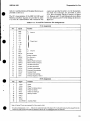
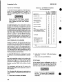
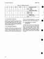
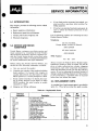
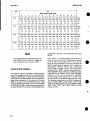
Programmable Peripheral Interface (PPI) devices to
control the board's six 8-bit I/O ports. Three ports
are interfaced through connector Jl and three are
interfaced through connector J2. Table 2-6 provides
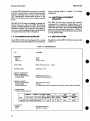
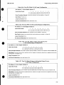
port and line identification of the two PPI devices.
Since each port may be programmed to suit several
applications, specific information pertaining to the
use of each port is provided in Chapter 3. Using one
port in a particular mode may impose restrictions on
another port. There are also certain jumper connections which are required for certain applications.
Refer to sections 3-13 through 3-22 forcompletePPI
programming instructions and jumper requirements.
•
•
•
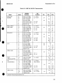
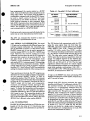
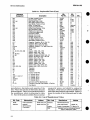
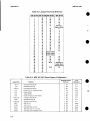
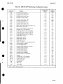
Lines which are used as outputs will require line
driver circuits for proper operation. Likewise, lines
which are used as inputs require terminator
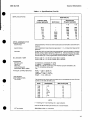
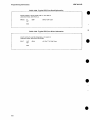
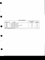
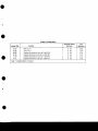
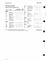
networks. Recommended line/driver and terminator devices are provided in table 2-7.
Unlike the other PPI ports, each bit of port E6 is
jumper connected to its driver/terminator socket pin
(U2, U3). This allows greater flexibility for port
configurations when using the on-board millisecond
timer (section 2-20), a power-fail configuration
(section 2-25) or an interrupt (section 3-20). The
jumper can also be used to reconfigure the bit order of
port E6.
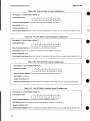
The iSBC 80/10B board is equipped with an on-board
failsafe timer. This timer is activated at the beginnig
of every CPU machine cycle. If an acknowledge is
not received within approximately 10 milliseconds,
the failsafe timer expires, and issues an acknowledge
signal, so the CPU may resume operation. If your
application does not require this feature, the
following modification must be performed:
Remove jumper 106 to 107
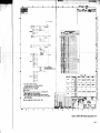
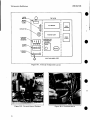
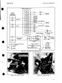
Figure 5-2, zone C7, gives the physical location of the
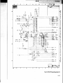
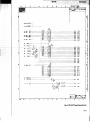
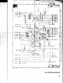
relevant jumper posts. They are also shown schematically in figure 5-3, sheet 4, grid location B4.
2-20. MILLISECOND TIMER
A millisecond timer may be implemented on-board
for use as a reference period. This timer does not
affect the baud rate clock or the failsafe timer. The
period of the millisecond timer, however, is affected
by the l10 baud jumper 80-81 (Fig. 5-3, Sheet 6). With
80-81 installed, the timer signal is low for 0.7ms
(l.4ms period). With 80-81 removed, the timer signal
is low for 1.0ms (2.0ms period). The timer may be
reset at any time by CTI, but if it is not reset it will
continue as a symmetrical signal with the period
described above. To implement the millisecond
timer:
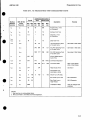
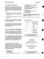
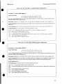
Port E4 is default configured to the output mode, with
a bus transceiver installed in socket Ul. Alternatively, the bus transceiver mode (input or output) can
be specified under program control by performing the
following modifications:
a.
a.
Remove jumper 59 to 60.
b.
b.
Install jumper 60 to 6l.
Port E6, bit 6 (PPI port C6) will then determine input
mode or the output mode. Refer to section 3-18 for
port C programming information.
To place the transciever in the input only mode,
remove jumper 59-60.
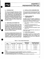
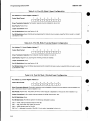
2-18. OPTIONAL RAM CONFIGURATION
If you install additional RAM devices on-board, the
following jumper modification is required for proper
memory addressing:
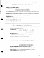
Install a jumper from timer output (post E15) to
the appropriate location. For example, timer
output may be connected to an 8255A port E6
input line, a port E6 output driver, or it may be
used as an interrupt source. Refer to Figure 5-3,
Sheet 7, zone C4.
'
Install a jumper from CTI (post Ell) to the
appropriate location which will control resetting
the timer. For example, CTI may be connected to
an 8255A port E6 output line, a port E6 input
terminator, or it may be tied low. Refer to Figure
5-2, Sheet 7, zone C4 .
The output of the timer may be verified at jumper
post 15. The clock output is generated at U27, pin 13
and is identified as MST (Millisecond Timer). Refer
to Figure 5-3, Sheet 6, zone C2. Jumper posts are
located between sockets U2 and U3 on the board.
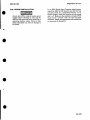
2-21. CONNECTOR INFORMATION
This modification indicates more than lK bytes of
RAM reside on-board.
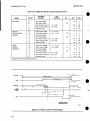
For systems applications, the iSBC BO/lOB board is
designed for installation into a standard Intel iSBC
604 or iSBC 614 Cardcage and Backplane assembly.
Alternatively, the board may be interfaced with a
design of your own choice, by means of an 86-pin
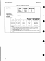
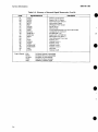
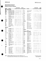
connector. Refer to table 2-10 for a list of suggested
manufacturers.
This jumper is shown on figure 5-2, and schematically on figure 5-3, sheet 4, zone C7.
Multibus signal characteristics and methods of
implementing a priority resolution scheme for bus
Install jumper 96 to 97.
•
2-19. FAILSAFE TIMER JUMPER
2-9