1
UM1818
Description
Figure 3. Three phase connection
The GP PLM module is provided of a user interface (J3) shown in Figure 4 where there are
connected the SPI interface pins (MOSI, MISO, SCK and NSS), the RS232 interface pins
(Tx and Rx), the USB interface pins (D+ and D-) and the user programmable general
purpose I/O pins. Remark that those pins are directly connected to the microcontroller, so be
careful to provide the correct insulation and
protection depending on the use those pins are addressed.
It is possible to power the PLM using the +3.3VDC (pin 19), +12VDC (pin 20 or 22) and
GND (pins 17, 23, 20 and 24) of this connector instead of the connector J2, using only a
single connector for power supply and control signals.
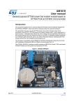
A lithium backup battery mounted on the board and 32 KHz quartz allows the use of the full
functionality of the internal RTC of the microcontroller, allowing precise time-based
operations.
Figure 4. User interface connector
J3
PLM_GPIO7
PLM_GPIO6
PLM_GPIO5
PLM_GPIO4
PLM_GPIO3
PLM_GPIO2
PLM_GPIO1
PLM_GPIO0
VCC
2
1
4
3
6
5
8
7
10
9
12
11
14
13
16
15
18
17
20
19
22
21
24
23
SPI_ MOSI
SPI_ MISO
SPI_S CK
SPI_ NSS
USART_RX
USART_TX
USB_ DP
USB_ DM
BOOT0
VDDIO
TSW-112-08-L-D- RA
GSPG23072015DI1045
A two color LED allows the signaling the board operations, data transmission and reception.
DocID026935 Rev 2
5/47
47