1
Rev. D
$15.00
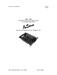
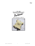
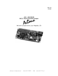
ANC - 1055
24 Channel Digital I/O
Pc Compatible Card
Antona Corporation, Los Angeles, CA
1643 ½ Westwood Blvd., W. Los Angeles, CA 90024 (310)473-8995 FAX (310) 473-7112
Antona Corporation
Copyright
Copyright 1992 by Antona Corporation. All rights reserved. no part of this
publication may be reproduced, transmitted, transcribed, stored in a retrieval system, or
translated into any language or computer language, in any form or by any means, electronic,
mechanical, magnetic, optical, chemical, manual or otherwise, without the prior written
permission of the Antona Corporation of Los Angeles, California.
Warranty
Antona Corporation products are warranted to be free from defects in materials and
workmanship for a period of one (1) year from the date of original shipment to customer.
This warranty is limited to the replacement or repair of parts not subjected to misuse,
neglect, unauthorized repair, alteration (except strap options), accident, or failure due to the
effects of static electricity discharge.
In no event shall Antona corporation be liable to the purchaser for loss of use, profit,
or consequential damages, or damages of any kind, including, but not limited to, accidental
loss or damage to other equipment, arising out of use of Antona Corporation equipment,
whether or not said equipment was used properly.
This warranty is in lieu of any other warranty, expressed, implied, or statutory,
including, without limitation, any implied warranty or merchantibility or fitness for a particular
purpose. No amendment of this warranty may be effected except in writing by an officer of
the Antona Corporation.
All repair services shall be performed at the Antona Corporation plant in Los Angeles
CA. THE PURCHASER MUST OBTAIN A RETURN AUTHORIZATION FROM THE
ANTONA CORPORATION PRIOR TO RETURNING ANY PIECE OF EQUIPMENT.
Shipment to the Antona Corporation will be at the expense of the of the purchaser. Return
shipment will be at the expense of the Antona Corporation for all warranty repairs.
1643 ½ Westwood Blvd., W. Los Angeles, CA 90024 (310)473-8995 FAX (310) 473-7112
Table of Contents
1.0 OVERVIEW ............................................................................................................................................................1
1.1 CARD INITIALIZATION .................................................................................................................................................1
1.2 INTERRUPT OPERATION ...............................................................................................................................................2
1.3 I/O PORT FUNCTION....................................................................................................................................................2
1.3.1 I/O PORT ADDRESSING.............................................................................................................................................2
2.0 CARD GENERAL HARDWARE INFORMATION.............................................................................................3
2.1 CARD HARDWARE OPTIONS ........................................................................................................................................4
2.1.1.0 CARD ADDRESS - 8-BIT SWITCH ...........................................................................................................................4
2.1.1.1 PAL TYPE SELECTION (JUMPER 1 AND 3) ..............................................................................................................4
2.1.1.2 PORT A DIRECTION (JUMPER 2)..............................................................................................................................4
2.1.1.3 INTERRUPT VECTOR SELECT (JUMPER 4) ................................................................................................................5
2.1.1.4 RIBBON CABLE CONNECTIONS (J1)........................................................................................................................6
2.1.1.5. USER SELECTED PORT BUFFERS/TERMINATORS ....................................................................................................7
3.0 SOFTWARE DESCRIPTION.................................................................................................................................7
APPENDIX A - SAMPLE CARD PROGRAMS............................................................................................................9
APPENDIX B - OPTO 22 PIN OUTPUTS ...................................................................................................................12
APPENDIX C - 8255 PERIPHERAL CONTROLLER CHIP.......................................................................................13
1643 ½ Westwood Blvd., W. Los Angeles, CA 90024 (310)473-8995 FAX (310) 473-7112
ii
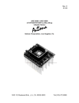
ANC-1055 IBM Pc/XT/AT Compatible Digital I/O Card
1.0 Overview
Providing 3-8 bit buffered TTL I/O channels, the ANC-1055 occupies a short card slot
in the IBM Pc, /XT or /AT computer. Programmable interrupt circuitry is provided to monitor
4 of the 24 channels to generate a user selectable, and software enabled, interrupt to the
IBM Pc. There are 3 separate modes of operation, all under software control, allowing
bidirectional, dedicated or strobed Input/Output operation. Additionally the ANC-1055 card
is directly pin connection compatible with the Opto 22, Crydom and Gordos lines of modular
relay boards to provide an industrial quality interface for control and monitoring applications.
Specifically, the ANC-1055 card is directly compatible with the PB16 and PB24 series units
with the appropriate interface cable (available from ANTONA as an ANC-CABL). The
designer should be aware that the pin numbers on the ANC-1055 J1 connector and the
control module numbers on the PB Series I/O Modules do not match. Refer to the technical
manual for the specific manufacturers module for input/output control signal designation.
Programming can be performed in ASSEMBLY LANGUAGE or by using English-like
INP/OUT commands in MS-DOS BASIC. The User's Manual included with the card
provides both BASIC and ASSEMBLY LANGUAGE source code which the designer may
use as a basis for develping his own device drivers.
1.1 Card Initialization
Upon system power-up the card's 8255 control register must be loaded with the
desired system configuration. A sample initialization program is included as Appendix A of
this manual.
The general procedure for initialization of the card is as follows:
1.
Initialization of the peripheral controller 8255 chip.
2.
Initialization o f the Control Latch to enable interrupt generation and data
direction flow of Port A, if used.
3.
If interrupts are used, enabling the selected bit on the 8259A interrupt
chip's mask
register located on the motherboard of the Pc to honor the
selected interrupt vector (see
IBM Technical Reference).
4.
Transfer control to start execution of user stored BASIC (or 8088
ASSEMBLY LANGUAGE program).
1643 ½ Westwood Blvd., W. Los Angeles, CA 90024 (310)473-8995 FAX (310) 473-7112
1
1.2 Interrupt Operation
The general procedure for using interrupts is as follows:
1.
Enable interrupts un der software control.
2.
When interrupt is requested, save all registers.
3.
Input status to determine source of interrupt-read 8255 to determine
interrupt source, if needed.
4.
Do interrupt service routine.
5.
Restore all registers, re-enable software interrupts and return to main
program.
The ANC-1055 can provide up to 4 interrupt inputs directed to any one of 5 user
selected interrupt vector locations. This means that the user can enable under software
control 0 to 4 individual interrupt sources, directed to a single interrupt vector location. The
user then inputs port C and port A of the 8255 and examines the proper bits to determine the
source of the interrupt. The user must set up the IBM Pc's interrupt controller chip (8259) in
addition to providing the appropriate interrupt hadling software.
1.3 I/O Port Function
The ANC-1055 has a variety of I/O modes. All of the modes can be directly
controlled under MS-DOS BASIC ir 8088 ASSEMBLY LANGUAGE. Appendix C is a
detailed specification of the 8255 Peripheral Controller Chip covering the various modes.
Basically, the user outputs a single control byte to control port D, which configures port A,B
and C to the desired mode.
There are 3 main modes of operation, allowing bidirectional I/O on port A, dedicated
I/O on ports A,B and C, with port C being capable of 4 bits each of input or output. The last
mode offers strobed Input/Output operation to latch input data and generate an interrupt or
status line to the 8088.
1.3.1 I/O Port Addressing
The following table details the address and function performed for I/O port operation.
CAR
DPO
RT
A
B
C
D
E
9 8
BIT WEIGHT
7 6 5 4 3 2 1 0
XX
XX
XX
XX
XX
XXXX
XXXX
XXXX
XXXX
XXXX
X
X
X
X
X
0
0
0
0
1
0
0
1
1
0
0
1
0
1
0
HEX VALUE
AS SHIPPED
300H
301H
302H
303H
304H
COMMENT
8-bit I/O port, LS645 buffer
8-bit I/O port, TTL sockets
8/(2-4)-bit I/O port, TTL sockets
Configuration Control Port
Interrupt Contol./Port A direction control
1643 ½ Westwood Blvd., W. Los Angeles, CA 90024 (310)473-8995 FAX (310) 473-7112
2
note that the "X"s are user selected bits set on the 8-bit switch on the ANC-1055 card.
The output/input bits are directed to the 50-pin ribbon connector located at the right
side of the ANC-1055 card, a ground and +5v connection are also provided at the
connector. See hardware connector section or schematic for pinouts.
The function of the individual bits on Port E are as follows:
Bit
Weight
0
1
2
3
4
5
6
7
Function
High level ("1") enables interrupt input on Port C, Bit 3
High level ("1") enables interrupt input on Port C, Bit 4
High level ("1") enables interrupt input on Port C, Bit 0
If jumper 2 enabled, will control direction of data flow to
LS645 on Port A - "1" for output, "0" for input.
High level ("1") enables interrupt input on Port A, Bit 7
- not used - not used Master Interrupt Enable Bit, "0" to enable, "1" to disable
This port should be set-up shortly after power-up, depending upon the user applications.
**** IMPORTANT - INTERRUPT INPUTS ARE DETECTED, DEPENDING ON HOW
THE USER INITIALIZED THE 8255, FOR LOW-GOING EDGE OR LOW-LEVEL INPUT.
THE PORT A BIT 7 INTERRUPT IS LOW-LEVEL INPUT ONLY.
2.0 Card General Hardware Information
The ANC-1055 is electrically and mechanically compatible with the IBM Pc/XT/AT.
Installation of the card within the mainframe of the Pc should be performed as detailed by
any of IBM's Inventory Checklists which explain adding circuit cards to the IBM Pc
motherboard. The procedure basically consists of:
1. Remove the power cord from the base unit.
2. Remove the screws on the back of the unit and pull forward the unit
cover.
3. Remove the metal plate at any unused card slot location.
4. Install the ANC-1055 Card (set card address before insertion).
5. Replace cover, screws and power cord last. Connect mating 50-pin
female ribbon cable connector to ANC-1055 at rear of unit.
1643 ½ Westwood Blvd., W. Los Angeles, CA 90024 (310)473-8995 FAX (310) 473-7112
3
2.1 Card Hardware Options
The following sections detail the use and changes of the strap options of the ANC1055. To properly identify the pin locations, place the card component side up with the
card's gold connector pointed towards you. The "common connection" designates where
one end of the jumper should always be connected to the desired card action or operation.
Some jumpers merely enable functions (like interrupt vector), while others allow selection of
hardware modes of operation. Some of the strap options may require a circuit trace on the
solder side of the card between pads to be cut with an X-Acto Knife or Dremel Tool.
2.1.1.0 Card Address - 8-Bit Switch
The switch can be set to occupy any address on the Pc from 000H to 3F8H in
increments of 8-addresses. When shipped, the card is set to address 300H. This means
that Port A is 300H, and all other ports are referenced from 300H
Figure 2.1
2.1.1.1 PAL Type Selection (Jumper 1 and 3)
These 2 jumpers are included to disable input to pins 12 and 19 of the U2 GAL
(jumpers included to maintain compatibility with previous versions of the ANC-1055 where a
PAL16L8CN was used). These jumpers allow the user to disconnect the external interrupt
from port A bit 7 (JP1) and port C bit 0 (JP3). User should not be concerned with
disconnecting these jumpers unless a PAL (not GAL) is in the U2 socket.
2.1.1.2 Port A Direction (Jumper 2)
This 3 pin jumper allows the user to select the source of direction control for port A. If
the jumper shorts posts "W" and "Y", then bit 3 of the Port E control latch controls
direction(as shipped). Port A must be configured for input normally and set to output in
response to the state of port C bit 6 level. If "Y" and "Z" jumper posts are shorted, then the
state of Port C bit 6 will control direction. Note that if Port C is an input port, then either an
external drive signal connected to the port C bit 6 pin, or the Port E bit 3 latch can control
the direction of data flow. Lastly, the user can install jumpers in both "V" to "Z" and "W" to
1643 ½ Westwood Blvd., W. Los Angeles, CA 90024 (310)473-8995 FAX (310) 473-7112
4
"Y" so that the Port E bit 3 signal can control direction and drive the Port C bit 6 when port
C is used in input mode.
2.1.1.3 Interrupt Vector Select (Jumper 4)
There are 5 vectors that can be chosen for the card to jump to when an interrupt is
generated. The schematic and the table below show what interrupt is generated.
VECTOR
PIN # (REV. B)
PIN # (REV. A)
IRQ2
IRQ3
IRQ4
IRQ5
IRQ7
2
3
4
5
7
5
2
1
3
4
The version B silk-screen artwork for the ANC-1055 has been changed so that the
single digit associated with the interrupt pin identifies the IRQ line on the Pc's bus.
1643 ½ Westwood Blvd., W. Los Angeles, CA 90024 (310)473-8995 FAX (310) 473-7112
5
2.1.1.4 Ribbon Cable Connections (J1)
The 50-pin I/O ribbon cable connector located on the ANC-1055 provides output
connection for all 24 lines. There is a ground line provided between each signal line, and a
+5v output line for signal pull-up, if required. The figure below details the port and bit
assigned to each pin.
Port A, Bit 0 -- 1
Port A, Bit 1 -- 3
Port A, Bit 2 -- 5
Port A, Bit 3 -- 7
Port A, Bit 4 -- 9
Port A, Bit 5 --11
Port A, Bit 6 --13
Port A, Bit 7 --15
Port C, Bit 0 --17
Port C, Bit 1 --19
Port C, Bit 2 --21
Port C, Bit 3 --23
Port C, Bit 4 --25
Port C, Bit 5 --27
Port C, Bit 6 --29
Port C, Bit 7 --31
Port B, Bit 0 --33
Port B, Bit 1 --35
Port B, Bit 2 --37
Port B, Bit 3 --39
Port B, Bit 4 --41
Port B, Bit 5 --43
Port B, Bit 6 --45
Port B, Bit 7 --47
+5 Volts(fused)-49
||
||
||
||
||
||
||
||
||
||
||
||
||
||
||
||
||
||
||
||
||
||
||
||
=========
o o || 2-o o || 4-o o || 6-o o || 8-o o || 10-o o || 12-o o || 14-o o || 16-o o || 18-o o || 20-o o || 22-o o || 24-o o || 26-o o || 28-o o || 30-o o || 32-o o || 34-o o || 36-o o || 38-o o || 40-o o || 42-o o || 44-o o || 46-o o || 48-o o || 50-=========
Ground
Ground
Ground
Ground
Ground
Ground
Ground
Ground
Ground
Ground
Ground
Ground
Ground
Ground
Ground
Ground
Ground
Ground
Ground
Ground
Ground
Ground
Ground
Ground
Ground
Figure 2.1
J1 50-pin ribbon cable I/O connector (viewed looking into connector)
1643 ½ Westwood Blvd., W. Los Angeles, CA 90024 (310)473-8995 FAX (310) 473-7112
6
2.1.1.5. User Selected Port Buffers/Terminators
There are 4 sockets located near the 50-pin connector which may be populated with
a variety of TTL compatible drivers or resister termination networks. When shipped, the
card is populated with 74S32 buffers - but note that any 74xx series part may be put into
these sockets for output buffering (i.e. 74S125 for tri-state, 74S00 for inverted output,
74S38 for open-collector buffering, etc.). Port A has an on-board LS245/LS645, to provide
input or output buffering. The chip is socketed so that the user may replace this part with a
74LS640 through 74LS644 for open collector, tri-state or inverted output/input. If any of the
three 8-bit ports requires a passive pull-up or pull down, a resister pack site is provided for
each port (RP2 for port A, RP3 for port C and RP4 for port B). The user may select the
resister value as appropriate to the application. Pin 1 of each resister pack site is connected
to +5 volts, and pin 10 is connected to ground (note RP4 pin 1 is located nearest the F1 fuse
and is fused through F1 See schematic ).
For input operation of ports B and C, the user may use 14-pin component headers a
provide a 1K resister pulled-up to +5v either installed in the resister packs or soldered onto
the component headers. For long line termination with a 220 ohm resister to +5v and a 330
ohm resister to ground. Note that because port C is programmable for 4-bits input/output,
that a buffer may be needed for 1 socket while a terminator header may be needed for the
input socket site.
The port bits are associated with the following sockets:
Port
B
B
Bits
0-3
4-7
14-Pin Socket
U8
U9
Comment
PT B LWR
PT B UPR
C
C
0-3
4-7
U6
U4
PT C LWR
PT C UPR
3.0 Software Description
The ANC-1055 may be controlled under MS-DOS BASIC or 80X86 Assembly
Language. The most common use is probably with BASIC, but in applications where speed
of operation is critical, Assembly Language may be the only choice. Note that a user may
write driver software that is "CALLed" from BASIC, or is completely interrupt driven and
operates as a background task or serviced when the attached device to the ANC-1055
signals through one of 4 interrupt lines.
Driver software may be divided into 3 basic tasks, initialization, reading and writing to
the card. Initialization should be performed as soon after power up as possible as the 8255
controller chip on the ANC-1055 will be configured a 3 input ports. The designer should
consider this factor if the ANC-1055 is intended for control application where drive signals
could be applied with the card uninitialized. A common practice is to have one output bit
assigned as a low enabled "system enable". In this way only after the card has been
initialized and the enable bit set low, will the control signals to the peripheral device under
control be honored. An alternate method is to use logic such that only when the ANC-1055
1643 ½ Westwood Blvd., W. Los Angeles, CA 90024 (310)473-8995 FAX (310) 473-7112
7
outputs a low signal on any of the port lines will the peripheral go into operation - called
"negative true logic". In all cases the designer is responsible for handling powerfail or other
computer problems. Once the digital input/output card is initialized, the user need only
format the 8-bit data to output and write it to the port for the write operation. Reading is
performed by inputting from the ports configured for input operation. This process may
sound complicated, but really is not. Examine the sample BASIC and Assembly Language
software drivers in Appendix A to get a better feel for the whole operation. Note that for AT
operation the user should not initialize and then read/write to a port in Assembly Language.
This is because at AT speeds the 8255 requires more time to configure itself then the
hardware can handle before the next command arrives. Solution - place a 'NOP'
instruction between initialization commands and reading/writing to the 8255.
1643 ½ Westwood Blvd., W. Los Angeles, CA 90024 (310)473-8995 FAX (310) 473-7112
8
Appendix A - Sample Card Programs
The following BASIC listing provides a sample software driver for card initialization,
reading and writing - it is a sample only and is not intended for resale by the purchaser or
end-user nor is it supported in any way by the Antona Corporation. It is supplied only as a
basis for the purchaser of the ANC-1055 to get an idea of the capabilities and features of
the card.
10 REM
20 REM
SET ANC-1055 UP FOR 24 OUTPUT BITS,
30 REM
THEN OUTPUT ALL POSSIBLE BITS PATTERNS
40 REM
TO EACH PORT A,B AND C
50 REM
CARD SET TO ADDR 300H (AS SHIPPED)
55 REM
60 A=&H300: B=A+1: C=A+2: D=A+3: E=A+4
70 REM
80 REM
SET PORTS TO OUTPUT, BUFFER ON PORT A TO OUTPUT
90 REM
100 OUT D,&HBC: OUT E,0
110 REM
120 REM
DO BINARY UP COUNT AND OUTPUT TO EACH PORT
130 REM
140 FOR X= 0 TO 255
150 OUT A,X: OUT B,X: OUT C,X
160 NEXT X
170 GOTO 140
180 END
-----------------------------------------------------------1000 REM
1010 REM A N T O N A CORPORATION
REV.1.1
1020 REM
1030 REM SAMPLE ANC-1055 INITIALIZATION,READ AND WRITE
1040 REM SUBROUTINES
1050 REM THE FOLLOWING MS-DOS BASIC PROGRAM LISTING
1060 REM PROVIDES 3 SIMPLE PROGRAMS WHICH READ IN AND
1070 REM WRITE OUT THE SAME BUFFER OF 1024 BYTES, THESE
1080 REM ROUTINES MAY BE USED AS SUBROUTINES FROM A MAIN
1090 REM PROGRAM WHICH INTERFACES WITH THE ANC-1055 CARD.
1100 REM
2000 DIM BUF%(1024)
2010 REM
2020 REM INITIALIZE ANC-1055 CARD
2030 REM
2040 A=&H300: B=A+1: C=A+2: D=A+3: E=A+4
2050 OUT D,&HBC: OUT E,0
2060 DUM=INP(A)
2070 RETURN
2080 REM
2090 REM READ IN A BUFFER OF 1024 CHARACTERS
2100 REM
2110 FOR X=0 TO 1023 2120 IF INP(C) AND &H20 THEN GOTO 2130 ELSE 2120
2130 BUF%(X)=INP(A)
1643 ½ Westwood Blvd., W. Los Angeles, CA 90024 (310)473-8995 FAX (310) 473-7112
9
2140 NEXT X
2150 RETURN
2160 REM
2170 REM WRITE OUT A BUFFER OF 1024 CHARACTERS
2180 REM
2190 FOR X=0 TO 1023
2200 OUT B,(BUF%(X) AND &HFF)
2210 IF INP(C) AND &H4 THEN GOTO 2210
2220 NEXT X
2230 RETURN
------------------------------------------------------------
Assembly Language Programs
The ANC-1055 may be driven directly by ASSEMBLY LANGUAGE with an increase
of operational speed up to 400:1 compared to a similar BASIC routine (as above). The
following programs detail how the ANC-1055 may be used to read/write to a data buffer
1024 characters long. The user will note that other functions would need to be performed in
order for these routines to be useful (i.e. loading buffer, setting up whatever peripheral is
being communicated with, etc.).
;
;EQUATES (BASED ON ANC-1055 CARD BASE ADDR OF 300H,AS SHIPPED)
;
PORTA
EQU
300H
;8 BIT PORT A (CHANGE AS APPROP)
PORTB
EQU
PORTA+1
;8 BIT PORT B
PORTC
EQU
PORTB+1
;8 BIT PORT C
CNTL
EQU
PORTC+1
;CONFIGURATION REG. OF 8255
PORTE
EQU
CNTL+1
;INTR. ENABLE/ PORT A DIRC.
;
; DATA BUFFER AREA
;
BUFFER
SEGMENT AT xxH ;BUFFER LOCATION DEFINED BY USER
DB
1024
;RESERVE 1024 LOCATIONS
;
; INITIALIZE ANC-1055 CARD
;
; WILL MAKE USE OF THE MODE 1 'HANDSHAKING' OPERATION OF THE 8255
; FOR INPUT.
;
INIT
MOV DX,CNTL
;SET UP CONTROL REG. ON 8255
MOV AL,0BCH
;SETS UP PORT A FOR INPUT, B FOR OUTPUT
OUT DX,AL
;(SEE APPENDIX C, P.10-180)
MOV
MOV
OUT
MOV
IN
DX,PORTE
AL,0
DX,AL
DX,PORTA
AL,DX
;SET LATCH FOR PORT A INPUT OPERATION
;AND DISABLE ALL INTERRUPT INPUT PINS
;(SEE P.4 OF MANUAL - PORT E)
;DO A DUMMY READ TO FLUSH CHARACTER ON
;POWER-UP
1643 ½ Westwood Blvd., W. Los Angeles, CA 90024 (310)473-8995 FAX (310) 473-7112
10
RET
;
; READ IN A BUFFER OF 1024 CHARACTERS
;
RD1055
PUSH AX
PUSH BX
PUSH CX
;SAVE ALL REGISTERS
PUSH DX
MOV BX,BUFFER ;BEGINNING OF WHERE DATA IS STORED
MOV CX,1024
;# OF CHARACTERS TO READ-IN
LOP1
MOV
IN
AND
JZ
DX,PORTC
AL,DX
AL,20H
LOP1
;USE TO SIGNAL WHEN DATA IS PRESENT
;READ IN STATUS BYTE
;JUST LOOK AT BIT
;NEXT CHARACTER HERE YET?
MOV
IN
MOV
DX,PORTA
AL,DX
[BX],AL
;SET UP TO READ PORT A
;GET BYTE
;STORE IN COMPUTER'S BUFFER
INC
DEC
JNZ
JMP
BX
CX
LOP1
EXIT
;INCREMENT BUFFER ADDRESS
;DECREMENT LOOP COUNTER
;GET NEXT BYTE, OR EXIT
;ALL DONE
;
; WRITE OUT A BUFFER OF 1024 CHARACTERS
;
WR1055
PUSH AX
PUSH BX
PUSH CX
;SAVE ALL REGISTERS
PUSH DX
MOV BX,BUFFER ;BEGINNING OF WHERE DATA IS STORED
MOV CX,1024
;# OF CHARACTERS TO READ-IN
LOP2
MOV
MOV
OUT
DX,PORTB
AL,[BX]
DX,AL
;SET UP TO WRITE PORT B
;GET BYTE FROM COMPUTER'S BUFFER
;WRITE BYTE TO PORT B
LOP3
MOV
IN
AND
JNZ
INC
DEC
JNZ
DX,PORTC
AL,DX
AL,04H
LOP3
BX
CX
LOP2
;USE TO SIGNAL WHEN DATA IS PRESENT
;READ IN STATUS BYTE
;JUST LOOK AT BIT
;DATA ACCEPTED YET?
;INCREMENT BUFFER ADDRESS
;DECREMENT LOOP COUNTER
;GET NEXT BYTE, OR EXIT
EXIT
POP
POP
POP
POP
RET
DX
CX
BX
AX
;RESTORE REGISTERS
;ALL DONE - EXIT TO CALLER
1643 ½ Westwood Blvd., W. Los Angeles, CA 90024 (310)473-8995 FAX (310) 473-7112
11
Appendix B - Opto 22 Pin Outputs
ANC-1055
J1
1
3
5
7
9
11
13
15
17
19
21
23
25
27
29
31
33
35
37
39
41
43
45
47
49
NOTE: 1.
OPTO-22
PB-24
1
3
5
7
9
11
13
15
17
19
21
23
25
27
29
31
33
35
37
39
41
43
45
47
49
OPTO-22
PB-16
OPTO-22
PB-8
17
19
21
23
25
27
29
31
33
35
37
39
41
43
45
47
49
33
35
37
39
41
43
45
47
49
RELAY
POSITIONS
23
22
21
20
19
18
17
16
15
14
13
12
11
10
9
8
7
6
5
4
3
2
1
0
+5VDC
PINS 2-50 ARE GROUND
1643 ½ Westwood Blvd., W. Los Angeles, CA 90024 (310)473-8995 FAX (310) 473-7112
12
Appendix C - 8255 Peripheral Controller Chip
The following pages provide an overview of the 8255 chip operation. Note that the
operation options, limitations, register definitions and input/output modes are all covered.
The IBM TECHNICAL REFERENCE (#6025005) is also an excellent source of information
on the 8259 Controller Chip. Of particular use are the pages showing I/O configurations
when the appropriate initialization word is output to the 8255.
NOTE: This Appendix is included with purchase of product.
1643 ½ Westwood Blvd., W. Los Angeles, CA 90024 (310)473-8995 FAX (310) 473-7112
13