1
Course Introduction
Purpose:
• The intent of this course is to give you a brief overview of the Freescale’s S08
Slave LIN Interface Controller (SLIC) module, including normal LIN operations
and special features such as high speed LIN mode and byte transfer mode.
Objectives:
• Describe basic LIN/SAE J2602 communications
• Describe how to connect the SLIC to the LIN bus
• Describe the SLIC modes of operation
• Describe how to use the SLIC to:
•
•
•
•
•
Handle LIN message transmissions & receptions
Use LIN synchronization data to re-trim local oscillators
Handle high speed LIN communications
Operate in low-power modes
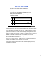
Content
51 pages
4 questions
•
Learning Time
75 minutes
TM
Freescale™ and the Freescale logo are trademarks of Freescale Semiconductor, Inc. All other product
or service names are the property of their respective owners. © Freescale Semiconductor, Inc. 2005.
The purpose of this course is to give you an overview of Freescale's S08 Slave LIN interface controller module -- also known
as the "SLIC Module." It will help you understand how to run normal LIN operations on the SLIC as well as special features
such as high-speed LIN mode and byte-transfer mode.
By the end of this course, you will be able to describe basic LIN and SAE J2602 communications, describe how to connect a
microcontroller with a SLIC module to a LIN bus, describe the SLIC modes of operation and describe how to use the SLIC to
handle LIN message transmissions and receptions, use LIN synchronization data to re-trim your local oscillators, handle
high-speed LIN communications and operate in low-power modes.
1
S08 SLIC features
• Full LIN message buffering of identifier and 8 data bytes
• Automatic bit rate and LIN message frame synchronization:
•
•
•
•
•
•
•
•
•
•
•
•
•
•
No prior programming of bit rate required, 1–20 kbps LIN bus speed
operation
All LIN messages will be received (no loss in synch process)
Input clock tolerance as high as ±50%, allowing internal oscillator to
remain untrimmed
Incoming break symbols always allowed to be 10 or more bit times
without message loss
Supports automatic software trimming of internal oscillator using LIN
synchronization data
Auto processing & verification of LIN SYNCH BREAK & BYTE
Auto checksum calculation & verification with error reporting
Enhanced checksum (includes ID) generation & verification
Maximum of 2 interrupts per LIN message frame
Full LIN error checking & reporting
High-speed LIN capability up to 83.33 kbps to 120.00 kbps
Configurable digital receive filter removes noise from the bus
Streamlined interrupt servicing with patented state vector register
Optional UART-like byte transfer mode (BTM) for non-LIN use
TM
Freescale™ and the Freescale logo are trademarks of Freescale Semiconductor, Inc. All other product
or service names are the property of their respective owners. © Freescale Semiconductor, Inc. 2005.
The SLIC module is a very powerful module with a great number of features. It contains full LIN message buffering
of the identifier and up to 8 data bytes at a time. It also handles LIN message-frame synchronization and
automatic bit-rate synchronization. It does not require pre-programming of the Baud rate for LIN-bus operation.
The SLIC handles all LIN messages including those during the synchronization process with no messages lost
due to the synchronization. It can handle input clock tolerances as great as plus or minus 50%, which allows you
to run off an internal oscillator and not even trim that oscillator, if that is so desired.
Incoming break symbols are allowed to be 10 or more bit times without the risk of message loss. The SLIC also
supports software trimming of the internal oscillator, if you so desire, based on synchronization data from the LIN
messages.
The synch break & byte are automatically processed by the SLIC and verified as valid. Checks on calculations are
done automatically and verified and if there's an error found, those are reported. The SLIC also supports
enhanced checksums which include the identifier that were introduced in LIN 1.3 and newer specifications. The
SLIC only interrupts the CPU two times for any LIN message frame -- always.
The SLIC also has full LIN error-checking and reporting. It's also capable of high-speed operation up to 120.00
kbps, which is six times faster than LIN specifies, but can be useful for programming in a factory environment.
On the receive pin, there's a digital receive filter that actually removes noise from the bus, rather than simply
flagging it for the software to decide what to do, which provides more robust noise suppression. Interrupt serviceroutine handling is streamlined through a patented state vector register to make interrupt service routines operate
more quickly. And, finally, there is a UART-like byte transfer mode for use primarily in non-LIN applications.
2
The LIN Short Story
• Targeted to be a lower performance (up to 20 kBit/s)
•
•
•
•
•
more cost effective solution than CAN
LIN is based on SCI / UART to help minimize system cost.
Communication rates up to 20kbps
Up to 15 slave-LIN nodes per Master
Can significantly reduce wiring cost & weight
Wiring = 3 Wires (Power + Ground + LIN data)
• Freescale is the only semiconductor company to be
a founding member of the LIN consortium
• Freescale products available TODAY:
>
>
>
>
>
Specific LIN Microcontroller Family
Master and Slave MCU’s.
Software drivers for HC12/08/05/S12
LIN physical Interface device (MC33661)
System Basis Chip with LIN Transceiver
(SBC LIN 33689 & SBC LIN Lite 33741)
> MCU + LIN + Smart power (MM908A62x products)
TM
Freescale™ and the Freescale logo are trademarks of Freescale Semiconductor, Inc. All other product
or service names are the property of their respective owners. © Freescale Semiconductor, Inc. 2005.
LIN was designed to be a low-performance, low-cost network -- lower cost than CAN networks and lower speed and lower
performance than CAN. It's based around a standard SCI or UART hardware to help minimize the costs.
Communications are 20kbps or slower and up to 15 slave nodes can be on any given LIN network with one single master.
LIN can help significantly reduce the wiring costs and weight. A single wire is used for the LIN communications, combined with a
battery level voltage supply and ground wire pair.
Freescale is the only semiconductor company that is part of the founding membership of LIN. Consequently, we have the ability to
vote on, and participate in, the design of the specifications. Freescale also has a wide variety of products available to create LIN
nodes: Everything from microcontrollers to physical layers, including system-basis chips and integrated products.
3
LIN / SAE J2602 Message Frame
Message Header
synch break
≥ 13 bit
Message Response
synch field identifier
FrameSynchronization
1 to 8 data bytes
Message
Descriptor
Bit-time
Synchronization
TM
checksum
Data Integrity
Message
Contents
Freescale™ and the Freescale logo are trademarks of Freescale Semiconductor, Inc. All other product
or service names are the property of their respective owners. © Freescale Semiconductor, Inc. 2005.
Let's begin by reviewing how LIN communicates, starting with the LIN message frame.
The synchronization-break character begins every LIN message frame. It provides frame synchronization so that when the bus is
idle, slave nodes can determine when a message frame begins. In LIN and J2602, it is required to be 13 or more bit times. This
guarantees that with oscillators that are less accurate at the slave nodes -- which are allowed to be plus or minus 14% -- those slave
nodes are guaranteed to see this as a valid break symbol.
The synch field – which provides bit-time synchronization - follows the synch break. The synch field is a FIVE-FIVE data character
which provides the greatest number of falling edges in a single character and it allows every slave the ability to dial in the bit rate of
the LIN message.
The identifier field, is next. It is a single byte that describes what the message frame means. These three symbols comprise the
message header which is transmitted from the master at all times. This is how the master is able to control communications on the
bus.
Next come the message contents. This is anywhere between 1 and 8 data bytes. This may come from a single slave or it may
come from the master and be sent to multiple slaves, solely as a checksum byte.
This checksum byte is calculated based on the data bytes and, in the case of the enhanced checksum, is also calculated based on
the identifier.
4
LIN / SAE J2602 Message Header
message header
synch break
≥ 13 bit
synch field identifier
• The Identifier logically describes the meaning of the message.
• The Identifier is protected with 2 Parity bits.
• There are up to 64 different Identifiers in a LIN system.
60 are freely available to a system designer. (0x00 – 0x3B)
4 are reserved for special purposes.
(0x3C – 0x3F)
• The master always sends this header, controlling when
messages appear on the bus.
TM
Freescale™ and the Freescale logo are trademarks of Freescale Semiconductor, Inc. All other product
or service names are the property of their respective owners. © Freescale Semiconductor, Inc. 2005.
The message header is sent by the master. The identifier byte is actually protected with a couple of parity bits at the end.
There are up to 64 possible identifiers in a LIN system because the first six bits in the identifier are selectable and the final two bits
are parity bits. Sixty of the 64 possible identifiers are available for general use. Four are reserved for special purposes; these are
3C, 3D, 3E, and 3F.
The master always sends this header information which allows you to have stable clocks and allows the master to control
communications on the bus.
5
Synchronization Break Field
Message Header
Message Response
break field
break TSYNBRK
syncdelimiter
TSYNDEL
sync field
Bit Time
TM
Freescale™ and the Freescale logo are trademarks of Freescale Semiconductor, Inc. All other product
or service names are the property of their respective owners. © Freescale Semiconductor, Inc. 2005.
Here is some of the terminology used in the LIN specification of the synchronization break field. There are some references to the
symbols and how they are measured in the LIN specification. Again, the synch break is actually part of the break field, which is
comprised of a synch break and a synch delimiter.
6
Synchronization Field
Message Header
Message Response
identifier
sync field
Start
Bit
0
TM
1
2
3
4
5
6
7
Stop
Bit
Freescale™ and the Freescale logo are trademarks of Freescale Semiconductor, Inc. All other product
or service names are the property of their respective owners. © Freescale Semiconductor, Inc. 2005.
The next character is the synchronization field. The synchronization field is critical in terms of determining the timing of the LIN
message frame. Again, it's a FIVE-FIVE data character which is sent out least-significant bit first. So you have five falling edges in
one character. This allows all slave nodes to measure the distance between these transitions, thus determining the LIN bus rate.
This combination of the break symbol and synchronization field is unique to LIN.
7
Identifier Field
Message Header
Message Response
identifier field
Start
Bit
ID0
ID1
ID2
ID3
ID4
ID5
P0
P1
0
1
2
3
4
5
6
7
Identifier Bits
TM
Stop
bit
Parity Bits
Freescale™ and the Freescale logo are trademarks of Freescale Semiconductor, Inc. All other product
or service names are the property of their respective owners. © Freescale Semiconductor, Inc. 2005.
The identifier field describes the message content and tells you what the message means. It is comprised of six identifier bits and
two parity bits. These parity bits help ensure the data integrity of the identifier.
8
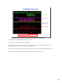
LIN Introduction
LIN Msg Header
LIN Data field
13bit Break Symbol
(w/ delimiter)
0x55
Synch
Symbol
Break /Synch same on all LIN msgs
TM
Msg ID byte
(0xC1)
ID defines
Msg
Freescale™ and the Freescale logo are trademarks of Freescale Semiconductor, Inc. All other product
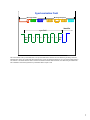
or service names are the property of their respective owners. © Freescale Semiconductor, Inc. 2005.
In these screen shots from an oscilloscope you can see the locations of the LIN message header and the data
field.
Here, the blue traces are the receive pin and the pink trace is the transmit pin of a LIN slave.
In the screen capture on the right, you can see a close-up of the header showing the break symbol, the
synchronization symbol, and the ID, which, in this case, is Value C1.
9
Data Field
Message Header
Message Response
Message Response
(data field)
In-Frame
Response
Space
Data
Byte 0
Data
Byte 1
…
Data
Byte n
Checksum InterField
Frame
Space
Interbyte Space
TM
Freescale™ and the Freescale logo are trademarks of Freescale Semiconductor, Inc. All other product
or service names are the property of their respective owners. © Freescale Semiconductor, Inc. 2005.
After the master has sent the message header, the message response field begins. The data contained in the message-response
field could be from a single slave or it could be from the master out to one or more slaves. This is simply UART-encoded 10-bit data
bytes: 8 bits with a start-bit and a stop-bit, as you will see in the next page.
10
Data Byte
Message Header
Message Response
data field
byte field
Start 0
Bit LSB
1
2
3
4
5
6
7 Stop
MSB Bit
8 Data Bits
TM
Freescale™ and the Freescale logo are trademarks of Freescale Semiconductor, Inc. All other product
or service names are the property of their respective owners. © Freescale Semiconductor, Inc. 2005.
Here you see how all data bytes are encoded as standard UART-data bytes. They are sent out least-significant bit first and are
preceded by a start-bit and ended with a stop-bit.
11
Checksum Field
Message Header
Message Response
checksum field
Start 0
Bit LSB
1
2
3
4
5
6
7 Stop
MSB Bit
8 Checksum Bits
TM
Freescale™ and the Freescale logo are trademarks of Freescale Semiconductor, Inc. All other product
or service names are the property of their respective owners. © Freescale Semiconductor, Inc. 2005.
Finally, the checksum is encoded in the same way. It begins with a start-bit, sent out least-significant bit first and ends with a stopbit. The checksum field ensures the data integrity of the message data and, in the case of the enhanced checksum, to ensure that
the message data matches the identifier.
12
Question
Which of the following statements about the LIN message frame
are accurate? Select all that apply and then click Done.
A. The synchronization field allows all slave nodes to measure
the bit rate of the LIN bus.
B. The identifier field is comprised of eight identifier bits and four
parity bits.
C The data contained in the message-response field of one LIN
message can only come from a slave device.
A. In the case of an enhanced checksum, the checksum field is
calculated based on the message data and the identifier.
Done
TM
Freescale™ and the Freescale logo are trademarks of Freescale Semiconductor, Inc. All other product
or service names are the property of their respective owners. © Freescale Semiconductor, Inc. 2005.
Take a moment to answer this question about the LIN message frame .
Correct.
The synchronization field allows all slave nodes to determine the LIN bus rate. The identifier field is comprised of six identifier
bits and two parity bits. The data contained in the message-response field could be from a single slave or it could be from the
master out to one or more slaves. The checksum field ensures the data integrity of the message data and, in the case of the
enhanced checksum, includes the identifier in the calculation to ensure proper pairing of the data and identifier.
13
MASTER & SLAVE Communications
(Master sends Data to one Slave)
Slave Node
Master Node
identifier
synch field
synch break
LIN Master
ID NOT recognized
quartz
Ignores data
(transmitting)
Slave Node
checksum
data byte
data byte
ID Recognized
Receives data
TM
Freescale™ and the Freescale logo are trademarks of Freescale Semiconductor, Inc. All other product
or service names are the property of their respective owners. © Freescale Semiconductor, Inc. 2005.
Now that we've looked at the details of one message frame, let's look at how message frames are used to pass
information around the LIN network
In this example, a LIN master is sending data to one slave. When header is sent out the top slave ignores it
because it does not recognize the ID. However, the bottom slave recognizes the identifier as a command
message and begins setting up to receive the data from the master.
The master then proceeds to send the data field and checksum, which are ignored. The bottom slave receives the
data and processes it.
14
MASTER & SLAVE Communications
(Sending multicast messages)
Slave Node
Master Node
identifier
synch field
synch break
LIN Master
ID Recognized
quartz
Receives data
(transmitting)
Slave Node
checksum
data byte
data byte
ID Recognized
Receives data
TM
Freescale™ and the Freescale logo are trademarks of Freescale Semiconductor, Inc. All other product
or service names are the property of their respective owners. © Freescale Semiconductor, Inc. 2005.
This is a similar example, however in this case the master is now communicating to multiple slaves.
The master sends out the header as before but, in this case, both slaves are programmed to understand and
receive that identifier. Thus, both slaves are set up to receive the data that's about to be sent by the master.
The master then sends out the message response containing data and checksum. Both slaves receive that data
and act accordingly.
15
SLAVE & MASTER Communications
(Polling SLAVES for data)
Slave Node
Master Node
identifier
synch field
synch break
LIN Master
data byte
checksum
quartz
data byte
• ID Recognized
NOT
• Slave
responds
Recognized
accordingly
• No
response
Slave Node
• ID Recognized
NOT
• Recognized
Slave responds
• No
accordingly
response
(receiving)
data byte
TM
data byte
checksum
Freescale™ and the Freescale logo are trademarks of Freescale Semiconductor, Inc. All other product
or service names are the property of their respective owners. © Freescale Semiconductor, Inc. 2005.
Here's an example of how a master would receive data from a slave. Again, the master sends out the header. In
this case, the top slave recognizes the identifier as one it will need to process.
The top slave responds because it recognizes the identifier as a request for data from that slave and sends back
data and a checksum. The bottom slave recognizes the identifier as an "Ignore" and does not respond.
Then when the master chooses to request data from the bottom slave, it sends out a header with a different
identifier. The bottom slave now recognizes this identifier and sends back a response; the top slave ignores this
second ID.
Two LIN slaves cannot respond at the same time during normal operations in a LIN system.
16
Automotive LIN Applications
•
•
•
•
HVAC actuators
Door systems
Lighting systems
Signal Indicators
TM
• Windshield wiper motors
• Headlight leveling motors
• Rainsensors
Freescale™ and the Freescale logo are trademarks of Freescale Semiconductor, Inc. All other product
or service names are the property of their respective owners. © Freescale Semiconductor, Inc. 2005.
Here are a couple of examples of where you might see LIN networks in an automotive application.
HVAC systems, with lots of actuators and dampers, as well as fan and temperature controls, are good examples.
These include car door systems containing window-lift motors, locks, switches, lighting systems, turn-signal
indications, full featured power mirrors, and so on.
You might also see LIN in power seats, windshield wiper motors, headlight leveling, rain sensors and a myriad of
other applications. These are primarily in the cabin of the vehicle where lower-speed networks are acceptable.
17
Non-Automotive LIN Applications
• Sensor & Actuator nodes for:
Distributed motor control
Remote switch panels
Paper and materials handling equipment
White goods (washing machines, dryers,
dishwashers, refrigerators)
TM
Freescale™ and the Freescale logo are trademarks of Freescale Semiconductor, Inc. All other product
or service names are the property of their respective owners. © Freescale Semiconductor, Inc. 2005.
LIN can also be used in non-automotive applications. Examples include anywhere you want to network a sensor
or an actuator for distributed motor controls, such as remote-switch panels, paper-handling equipment, and white
goods like washers, dryers, and refrigerators. Any machine where you might have a network of sensors and
actuators that could operate at lower speeds are suitable applications for LIN.
18
Connecting a LIN Slave to the bus
Analog/Power
MCU
PCB
VBatt
Vdd
Power
Conditioning
LIN Bus
Gnd
MC33661
Connector
LIN Physical
Interface
LIN
Gnd
9S08EL32
Tx
Rx
SLIC
Load
Driver
Device(s)
Load
Connector
Vdd
RESET and
IRQ
Gnd
TM
Freescale™ and the Freescale logo are trademarks of Freescale Semiconductor, Inc. All other product
or service names are the property of their respective owners. © Freescale Semiconductor, Inc. 2005.
The basic elements required to connect a LIN slave to a network are very simple. You need some sort of a
microcontroller or logic device that can communicate the LIN protocol. You also need some sort of powerconditioning circuitry to provide correct voltage and power protection to that device. The vehicle battery voltage
supply level is generally 8 to 18 volts, which is also the same maximum voltage level for the LIN bus according to
the LIN specification. You may also need load driver and interfacing devices to connect to sensors or actuators.
Most importantly, the transmit-and-receive pins of your logic device need to go through a LIN physical interface in
order to convert the electrical signals to a valid LIN bus signal.
19
Connecting a LIN Slave to the bus
Analog/Power
MCU
VBatt
PCB
LIN Bus
MC33689
Vdd
Power
Conditioning
Gnd
Gnd
Connector
LIN
LIN Physical
Interface
9S08EL32
Tx
Rx SLIC
Load
Driver
Device(s)
Load
Connector
RESET and
IRQ
LIN System Basis Chip
TM
Freescale™ and the Freescale logo are trademarks of Freescale Semiconductor, Inc. All other product
or service names are the property of their respective owners. © Freescale Semiconductor, Inc. 2005.
This is an example of how those analog circuits can actually be condensed into a single device such as, the LIN
System Basis Chip from Freescale. This combines the power-conditioning circuitry, external re-set controls and
various other switches and inputs with the LIN physical interface, to provide a much more integrated solution for
power-conditioning and interfacing to a logic device or microcontroller.
20
Question
True or false? A LIN system can have two LIN slaves responding
at the same time during normal operations.
Select your answer and then click Done.
A. True
B. False
Done
TM
Freescale™ and the Freescale logo are trademarks of Freescale Semiconductor, Inc. All other product
or service names are the property of their respective owners. © Freescale Semiconductor, Inc. 2005.
Answer this question about the LIN communications.
Correct.
Two LIN slaves cannot respond at the same time during normal operations in a LIN system. There is an exceptional case,
called out in the LIN specifications as “Event Triggered Frames”, which are unlikely to be used in most normal LIN systems.
21
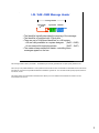
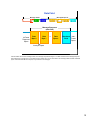
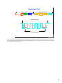
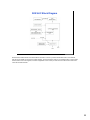
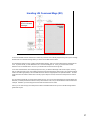
S08 SLIC Block Diagram
TM
Freescale™ and the Freescale logo are trademarks of Freescale Semiconductor, Inc. All other product
or service names are the property of their respective owners. © Freescale Semiconductor, Inc. 2005.
Now that we've looked at basic LIN communications and how to connect up a microcontroller with SLIC to a LIN network,
let's get into the details of how the SLIC module operates. The SLIC module is made up of a message buffer, a protocol state
machine, status-and-control registers, as well as a digital filter on the receive pin which removes noise from the LIN bus as it
comes into the state machine.
22
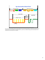
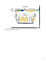
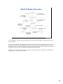
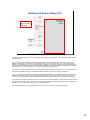
S08 SLIC Modes of Operation
TM
Freescale™ and the Freescale logo are trademarks of Freescale Semiconductor, Inc. All other product
or service names are the property of their respective owners. © Freescale Semiconductor, Inc. 2005.
The SLIC operates in a number of modes but primarily in its run state and low-power states. Let's take a quick look at the
modes of operation.
On most microcontrollers the SLIC module will come up in the SLIC re-set state. If the device is powered down, of course, it
goes into power-off state. Once the initialization routines are run on the SLIC module, it is taken from its reset state to its
disabled state, then to its enabled state by setting the SLIC enable bit. This is where it lives most of its life, communicating on
the LIN bus in the SLIC-run state. The details of each register will be discussed shortly.
Depending on the desired operation in low power, the SLIC can also be put into a stop or a wait state, to be awakened by
network activity or a re-set of the microcontroller.
23
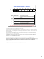
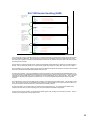
SLIC Register Overview
SLCC1
R
Bit7
Bit6
0
0
R
WAKETX
TXABRT
/ Configuration
Bit1
Bit0
IMSG
SLCIE
0
R
0
BT14
R
BT7
W
SLCS
Bit2
0
W
SLCBTL
Bit3
(Set it and forgetRXFP
it for most applications…some
exceptions)
SLCWCM
BTM
SLCE
W
SLCBTH
Bit4
INITREQ
BEDD
Initialization
W
SLCC2
Bit5
R
OptionalBT12
Status BT11
Information
BT13
BT10
BT9
(for re-trimming internal oscillator in LIN systems
BT6or controlling
BT5
BT4 rate in
BT3
BT2
BT1
bit
BTM operation)
0
SLCACT
0
0
0
BT8
BT0
0
INITACK
SLCF
W
SLCSV
R
0
0
I3
I2
I1
I0
0
0
TXGO
CHKMOD
DLC5
DLC4
DLC3
DLC2
DLC1
DLC0
R0
W
SLCDLC
Interrupt Status & Control Information
R
W
SLCID
SLCD0SLCD7
R
R7
R6
R5
R4
R3
R2
R1
W
T7
T6
T5
T4
T3
T2
T1
T0
R
R7
R6
R5
R1
R0
T6
T5
T1
T0
W
TM
T7
Message
Buffer
R4
R3
R2
T4
T3
Freescale™ and the Freescale logo are trademarks of Freescale Semiconductor, Inc. All other product
or service names are the property of their respective owners. © Freescale Semiconductor, Inc. 2005.
T2
There are seven registers in the SLIC module that control activity, with an additional nine registers for message buffering.
The first two registers are SLIC control registers and are primarily for initialization and configuration. These are largely setand-forget for most applications. There are a few exceptions on a few bits. We'll look at those in a minute.
The next two registers are the bit-time registers. These are optional status registers that are useful in LIN operations for retrimming your internal oscillator but are not required for normal LIN operations. They are used to control the bit-rate in bytetransfer mode operation.
Next are the status, state vector and data-length control registers. These are the heart of your interrupt service routines and
the heart of controlling the SLIC module. They give important status information as to the source of SLIC interrupts, as well
as controlling how message buffers are read.
And, finally, the last nine bytes are the SLIC message buffer, which is a single-byte buffer for the identifier and, then, eight
bytes for the data field.
24
SLIC Control Register 1 (SLCC1)
SLCC1
R
Bit7
Bit6
0
0
Bit5
Bit4
Bit3
Bit2
Bit1
Bit0
INITREQ
BEDD
WAKETX
TXABRT
IMSG
SLCIE
W
INITREQ
Initialization Request
Request initialization mode immediately
BEDD
Bit Error Detection Disable
Turns off bit error detect circuitry for BTM mode and high-speed LIN
operations.
WAKETX
Transmit Wakeup Symbol
Set this to send a wakeup signal pulse on the bus.
TXABRT
Transmit Abort Message
Aborts current transmission at next byte boundary.
IMSG
SLIC Ignore Message Bit
Once the LIN header is processed, and software decodes the ID,
you can set this bit to ignore the data field and prevent the second
interrupt for the end of the LIN message frame.
SLCIE
SLIC Interrupt Enable
enables interrupts based on SLCF flag.
Refer to S08 SLIC chapter of the device user manual for exact bit descriptions and details.
TM
Freescale™ and the Freescale logo are trademarks of Freescale Semiconductor, Inc. All other product
or service names are the property of their respective owners. © Freescale Semiconductor, Inc. 2005.
So let's look at the status-and-control registers for the SLIC module.
The first control register has an initialization request bit. This bit places the SLIC module into its re-set state or allows it to
leave its re-set state. An acknowledge bit is in the status register. We'll look at this in a moment. This bit is a mirror of the
initialization request bit.
There is a bit to control bit-error detection circuitry. To be able to turn that circuitry on or off, that's very useful for bytetransfer mode as well as high-speed LIN operations.
The WAKETX bit allows you to send a wake-up signal on the bus. This is the only symbol that the SLIC is allowed to
transmit on a LIN bus without first receiving a header.
There is also a transmit-abort bit which allows you to abort a current transmission on the next byte boundary.
Next is the "Ignore Message" bit which allows you to ignore the data field of a LIN message frame. As we saw before, once
the header is received from the master, the ID byte determines what the message frame means. The slave can then choose
whether or not that identifier is important to it and, if not, the IMSG-bit can be used to ignore the data field and the
subsequent interrupts.
Finally is the interrupt-enable bit that enables the interrupt for the SLIC module.
25
SLIC Control Register 2 (SLCC2)
Bit7
SLCC2
R
Bit6
Bit5
Bit4
Bit3
Bit2
0
Bit1
Bit0
0
RXFP
SLCWCM
BTM
SLCE
W
RXFP
Receive Filter Prescaler
These are used to set the clock speed (thus the size of the digital
filter) for the receive pin. These should be adjusted for high-speed
LIN operation and BTM operation and may need to be set for
normal LIN operations.
SLCWCM
SLIC Wait Clock Mode
This bit controls whether or not the clocks continue to run in the
SLIC when the CPU goes into wait mode.
BTM
UART Byte Transfer Mode
This bit switches the SLIC between BTM and LIN modes. BTM
mode is useful when individual byte transfers are required in nonLIN systems.
SLCE
SLIC Module Enable
The bit turns the SLIC on and off.
Refer to S08 SLIC chapter of the device user manual for exact bit descriptions and details.
TM
Freescale™ and the Freescale logo are trademarks of Freescale Semiconductor, Inc. All other product
or service names are the property of their respective owners. © Freescale Semiconductor, Inc. 2005.
The second control register has controls for the digital-receive filter. These bits allow you to control the filter delay of the
digital-receive filter which allow you to control the width of the noise pulse that is blocked by this filter.
A wait-clock mode bit controls whether or not clocks are allowed to run in the SLIC module when the CPU goes into its wait
mode.
The BTM-bit is in the second control register to allow you to switch back and forth between BTM mode and LIN-operation
mode.
Finally, the SLIC-enable bit turns the SLIC module on or off.
26
SLIC Bit Time Registers (SLCBTH-L)
Bit7
SLCBTH
R
Bit6
Bit5
Bit4
Bit3
Bit2
Bit1
Bit0
BT14
BT13
BT12
BT11
BT10
BT9
BT8
BT6
BT5
BT4
BT3
BT2
BT1
BT0
0
W
SLCBTL
R
BT7
W
BT[14:0]
Bit Time Value
In LIN mode, this 15 bit number is updated every time a LIN header
is successfully processed. The value is the number of SLIC clock
cycles counted in a single bit time as measured in the LIN synch
byte. This count can be used to measure if the SLIC clock when
compared to an expected count. The internal oscillator can then be
adjusted accordingly (if applicable) to compensate for any
frequency changes.
In BTM mode, this number is updated by user software and controls
the number of SLIC clocks that make up a single bit, thus setting
the BTM bit rate.
Refer to S08 SLIC chapter of the device user manual for exact bit descriptions and details.
TM
Freescale™ and the Freescale logo are trademarks of Freescale Semiconductor, Inc. All other product
or service names are the property of their respective owners. © Freescale Semiconductor, Inc. 2005.
The bit-time registers are located after the control registers. They allow you to understand how many SLIC clock-cycles are
measured per bit-time in a valid LIN header. This information can be used to re-trim your local oscillator if you are running in
LIN mode.
27
SLIC Status Register (SLCS)
Bit7
SLCS
R
Bit6
Bit5
0
SLCACT
Bit4
Bit3
Bit2
Bit1
0
0
0
0
INITACK
Bit0
SLCF
W
SLCACT
SLIC Active
(Oscillator Trim Blocking
Semaphore)
This flag helps the user to understand if a LIN message header is
currently being processed, when oscillator trimming may affect
communications with the LIN bus. It can remain set at times other
than during processing of a LIN header.
INITACK
Initialization Mode
Acknowledge
This is the acknowledgement flag for the INITREQ bit in SLCC1.
SLCF
SLIC Interrupt Flag
This is the interrupt flag for the SLIC module. It indicates that an
interrupt request is pending, and the details of the source of that
request can be found by reading the SLCSV register.
Refer to S08 SLIC chapter of the device user manual for exact bit descriptions and details.
TM
Freescale™ and the Freescale logo are trademarks of Freescale Semiconductor, Inc. All other product
or service names are the property of their respective owners. © Freescale Semiconductor, Inc. 2005.
The SLIC-status register contains a few important status bits and the interrupt flag.
The SLIC-active bit is useful if you're doing local trimming of your oscillator. It'll help you to understand if that message
header is currently being processed or not so that you can decide whether it's safe to re-trim your oscillator. If you were to retrim your oscillator while receiving a LIN message header, it's possible that you could corrupt the reception of that header
with substantial changes to your local time base.
As mentioned previously, the initialization mode acknowledge bit is located here. This is just a mirror for the initializationrequest bit to let you know that initialization mode has been entered or exited.
Finally, the SLIC-interrupt flag is located in this register. This flag has to be cleared in order to finish an interrupt-service
routine and clear any pending interrupts. Once cleared, the SLIC State Vector register might be updated if any additional
interrupt sources are pending. We’ll look more at the SLIC State register on the next few pages.
28
SLIC State Vector Register SLCSV
SLCSV
R
Bit7
Bit6
Bit5
Bit4
Bit3
Bit2
Bit1
Bit0
0
0
I3
I2
I1
I0
0
0
W
This register tells the user software the source of the SLIC interrupt.
The sources are presented to the user in priority order, if multiple
interrupts are pending.
I [3:0]
Interrupt State Vector
The patented arrangement of this register allows the user to build
an efficient jump table to service the interrupts and begin servicing
all interrupt sources in equal execution time.
In LIN mode, there are 13 possible interrupt sources.
In BTM mode, there are 8 possible interrupt sources.
Refer to S08 SLIC chapter of the device user manual for exact bit descriptions and details.
TM
Freescale™ and the Freescale logo are trademarks of Freescale Semiconductor, Inc. All other product
or service names are the property of their respective owners. © Freescale Semiconductor, Inc. 2005.
The SLIC-state vector register is the next register in the memory map. This is one of the most important registers for the
SLIC module. It's set up with a patented arrangement of bits to encode the source of your interrupt and prioritizes these
sources for you. Every time this register is read, the most important, highest priority interrupt source is presented to the
software. We'll look at why this register is set up the way it is in just a moment. In LIN mode, you have up to 13 possible
interrupt sources. In BTM mode, there are eight possible interrupt sources.
29
SLCSV Register – LIN Mode
SLCSV
Bit7
Bit6
Bit5
Bit4
Bit3
Bit2
Bit1
Bit0
0
0
I3
I2
I1
I0
0
0
R
W
SLCSV
I3
I2
I1
I0
Interrupt Source
Priority
0x00
0
0
0
0
No Interrupts Pending
0 (Lowest)
0x04
0
0
0
1
No-Bus-Activity
1
0x08
0
0
1
0
TX Message Buffer Empty
Checksum Transmitted
2
0x0C
0
0
1
1
TX Message Buffer Empty
3
0x10
0
1
0
0
RX Message Buffer Full
Checksum OK
4
0x14
0
1
0
1
RX Data Buffer Full
No Errors
5
0x18
0
1
1
0
Bit-Error
6
0x1C
0
1
1
1
Receiver Buffer Overrun
7
0x20
1
0
0
0
Reserved
8
0x24
1
0
0
1
Checksum Error
9
0x28
1
0
1
0
Byte Framing Error
10
0x2C
1
0
1
1
Identifier Received Successfully
11
0x30
1
1
0
0
Identifier Parity Error
12
0x34
1
1
0
1
Reserved
13
0x38
1
1
1
0
Reserved
14
0x3C
1
1
1
1
Wakeup
15 (Highest)
Normally this is the 2nd interrupt in handling a LIN master
request message. (SLIC was transmitting data in a LIN frame)
Normally this is the 2nd interrupt in handling a LIN master
command message. (SLIC was receiving data in a LIN frame)
Normally this is the 1st interrupt in handling a LIN message.
Refer to S08 SLIC chapter of the device user manual for exact bit descriptions and details.
TM
Freescale™ and the Freescale logo are trademarks of Freescale Semiconductor, Inc. All other product
or service names are the property of their respective owners. © Freescale Semiconductor, Inc. 2005.
Let's take a quick look at LIN operations with the SLIC-state vector register.
The SLIC-state vector register interrupt-encoding bits are located in Bits 2 through 5. The reason for this will become
obvious in just a moment. These bits encode the 13 possible interrupt sources in LIN operations. In most LIN messageframe processing, you'll see three primary interrupts sources. If you look in this table, you'll see value 2C is the interrupt
source that indicates you've successfully received an identifier. This means you've received a complete LIN message
header and the ID parity bits are valid.
At this point, you can determine what to do with the rest of the message frame based on the value in the SLIC ID register. If
you're receiving data, then you will proceed to set up to receive that data. The next interrupt you see will be Value ONE
ZERO. It tells you that the LIN message receive buffer is full and the incoming checksum was valid.
If you read the identifier and the message is to be transmitted, you'll load up the transmission buffer and proceed to transmit
the data. The second interrupt you receive in a properly-transmitted message will be Value ZERO EIGHT. This tells you that
the buffer has been sent and a checksum has been transmitted.
30
SLIC Data Length Code Reg SLCDLC
SLCDLC
R
Bit7
Bit6
Bit5
Bit4
Bit3
Bit2
Bit1
Bit0
TXGO
CHKMOD
DLC5
DLC4
DLC3
DLC2
DLC1
DLC0
W
TXGO
SLIC Transmit Go
This bit tells the SLIC start transmitting the contents of the message
buffer. It gets set after the buffers are loaded by user software and
sends out the number of bytes indicated by the DLC bits.
LIN 1.3 and newer allows for 2 different checksum calculations on
any message frame.
CHKMOD
LIN Checksum Mode
This bit controls whether the ID byte is included in the checksum
calculation or not, corresponding to the enhanced or classic
checksum calculations.
These bits tell the SLIC how many bytes to transmit (for LIN master
request messages) or how many bytes to expect to receive (for LIN
master command messages).
DLC[5:0]
Data Length Control Bits
The SLIC allows this length to exceed the LIN normal message limit
and be set up to 64 bytes to allow extended frame messages to be
processed while only interrupting the CPU every 8 bytes.
Refer to S08 SLIC chapter of the device user manual for exact bit descriptions and details.
TM
Freescale™ and the Freescale logo are trademarks of Freescale Semiconductor, Inc. All other product
or service names are the property of their respective owners. © Freescale Semiconductor, Inc. 2005.
Once you've received a LIN header, you have to look at the ID and determine whether you're transmitting or receiving data.
That data is contained in the message buffers, but the information on how to interpret the message-buffer data is contained
in the data-length code register.
The data-length code register is broken down into three components: The transmit-go bit allows you to immediately initiate
transmitting the data in the message buffers. In the case of reception of data, the TX-GO bit will be written as a ZERO.
The checksum-mode bit tells you which checksum calculation to use: the one that does include the identifier or the one that
does not include the identifier.
Finally, the data-length control bit tells the SLIC how many bytes of data in the message buffers are expected to be received
or should be sent. In normal LIN-message frames this will be a value from 1 to 8. However, there are enough bits in the
data-length control to encode up to 64 bytes to handle extended message frames.
31
SLIC Identifier & Data Registers
SLCID
SLCD0SLCD7
SLCID
Bit7
Bit6
Bit5
Bit4
Bit3
Bit2
Bit1
Bit0
R
R7
R6
R5
R4
R3
R2
R1
R0
W
T7
T6
T5
T4
T3
T2
T1
T0
R
R7
R6
R5
R4
R3
R2
R1
R0
W
T7
T6
T5
T4
T3
T2
T1
T0
SLIC Identifier Register
In LIN mode, this register is updated automatically with the value of
the identifier contained in the received LIN message header. This
ID value is then generally used on the second LIN message
interrupt also, to determine how to process a received message or
handle the completion of transmitted message.
In BTM mode, this register is used as a transmit and as a receive
buffer.
This is the data buffer for SLIC. The number of valid bytes for any
given message is determined by the DLC bits in the SLCDLC
register. Checksum bytes are not recorded in the data registers.
SLCD0-7
SLIC Data Registers
This buffer receives data bytes from the LIN bus for LIN master
command messages.
It is loaded by user software with data to be transmitted in LIN
master request messages.
Refer to S08 SLIC chapter of the device user manual for exact bit descriptions and details.
TM
Freescale™ and the Freescale logo are trademarks of Freescale Semiconductor, Inc. All other product
or service names are the property of their respective owners. © Freescale Semiconductor, Inc. 2005.
Finally, in the registers for the SLIC module, you will see the message-buffer registers. This is a SLIC-ID register as well as
the data registers, 0 through 7.
The ID register in LIN mode contains the ID of a valid received LIN header. This is used to make decisions based upon the
value of the ID as to how to process the subsequent interrupts. In BTM mode, the ID register is used as the primary sendand-receive buffer for each byte.
The SLIC-data registers contain the LIN message data and only the number of bytes encoded in the previous register, the
DLC register, are valid in the data registers at any given time.
32
Initializing the SLIC– LIN Mode
The steps for SLIC Initialization for LIN operation are:
1. Write SLCC1 to clear INITREQ
2. When INITACK = 0, write SLCC1 & SLCC2 with desired values for:
a) BEDD – Use to disable bit error detect in high speed LIN mode
b) SLCWCM - Wait clock mode
c) RXFP - Digital receive filter clock prescaler
3. Enable the SLIC module by writing SLCC2:
a) SLCE = 1 to place SLIC module into run mode
b) BTM = 0 to disable byte transfer mode
4. Write SLCC1 to enable SLIC interrupts (if desired)
TM
Freescale™ and the Freescale logo are trademarks of Freescale Semiconductor, Inc. All other product
or service names are the property of their respective owners. © Freescale Semiconductor, Inc. 2005.
So now that we've looked at the registers for the SLIC module, let's take a look at how you set the SLIC module up for LIN
operation.
First, you clear the initialization-request bit. Once the corresponding acknowledge bit is cleared you know that the module
has left re-set mode.
You then need to write values into the control registers with your desired settings for bit-error detection disable, wait-clock
mode, and the prescaler for the digital-receive filter.
Finally, enable the SLIC module by writing the SLIC-enable bit to move the SLIC module into its run mode.
And, if interrupts are desired, you'll want to set the interrupt-enable bit in Control Register 1.
33
8-byte LIN Message Interrupts
Bit-Banged LIN Slave (~100-120)
TM
UART LIN Slave
(12)
SLIC LIN Slave
(2)
Freescale™ and the Freescale logo are trademarks of Freescale Semiconductor, Inc. All other product
or service names are the property of their respective owners. © Freescale Semiconductor, Inc. 2005.
So let's take a quick look at an 8-byte LIN request message and compare how interrupts are handled in various types of LIN
slave devices.
On the top line, Trace 1, you can see a typical LIN message. In this case, it's an 8-byte LIN request message. So the data
is being provided by the LIN slave.
The first line you see below the LIN message frame is a bit-banged LIN slave. Notice how many interrupts are being
serviced here. Depending on how the bit-banged LIN slave is written, you may have upwards of 100 to 120 interrupts permessage frame. This depends on whether the bit-banged LIN slave is operating based on edges or based on every-bit time.
Nevertheless, it's a lot of interrupts for one message.
So, comparing that to a normal UART operation for this 8-byte LIN message, you see a drastic reduction in interrupts using
just a UART. You get down to 12 interrupts, basically one for every symbol in the message. You have a 3-symbol header,
followed by up to 8 data bytes and a checksum byte.
But if you take a look at comparing that to how the SLIC operates, you can see that the SLIC only has two interrupts to
process. Essentially, there is one for the header and one for the message field. This is true regardless of message content,
unless you invoke the Ignore message feature, where only one interrupt occurs.
34
Basic SLIC Interrupts – LIN Operation
For messages of interest:
1st Interrupt – Already synchronized
Perform ID decode
Load TX data and send (if TX)
LIN Header
LIN Data field
2nd Interrupt – Data & Checksum TX complete
RX Data Ready (if RX)
LIN Header
Data
For messages to be ignored:
1st Interrupt – Automatically synchronized
Perform ID decode
Ignore rest of message
No interrupts until new frame
TM
Freescale™ and the Freescale logo are trademarks of Freescale Semiconductor, Inc. All other product
or service names are the property of their respective owners. © Freescale Semiconductor, Inc. 2005.
Let’s look at those two interrupts in a little bit more detail. Here you see the receive line is in the center and the transmit line is in the
bottom because these are relative to the slave. Because the transmit line is active, you can see that this LIN slave is providing the
data on the bus. The top line shows the interrupts for the SLIC module. So after the master node has sent the LIN header, you
receive your first interrupt.
This interrupt tells you that the SLIC module has already synchronized to the message frame and, then, to the bit rate. It has received
the identifier and checked its parity bits. If the slave node desires to send data, which, in this case, it does, this data is then loaded
into the transmit buffers and then the TX go-bit is set.
The data field is next. Notice that the SLIC module is transmitting data out on to the bus. At the end of that data transmission comes
the second interrupt. This interrupt tells you that the data and the checksum transmission are complete. If this was a reception of
data, this interrupt would tell you that the data has been received properly and the checksum is verified properly.
Let’s return to the previous discussion of "ignored" messages. Messages to be ignored can be processed with only one interrupt.
Once the header arrives you receive this interrupt.
This means that the header has been properly processed, which means the identifier has correct parity. However, once the slave
performs a software look-up on this identifier and determines that it does not need to respond to this message, the IMSG-bit is set.
The data that comes in after that header is completely ignored and no second interrupt occurs.
35
Handling LIN Message Headers
Typical ISR
flow for LIN
header.
ISR flow for ignored messages.
TM
Freescale™ and the Freescale logo are trademarks of Freescale Semiconductor, Inc. All other product
or service names are the property of their respective owners. © Freescale Semiconductor, Inc. 2005.
Let's look a little bit more in detail on how these interrupts are actually processed.
Again, the first interrupt is designed to handle a LIN message header. This assumes, of course, LIN operation. Here is a flow
diagram that illustrates the basic flow of the first interrupt in processing a LIN message.
The typical flow of the interrupt service routine is straight down the flow chart. The header is received, is determined to be
valid, the SLIC updates to the bit-time registers, and the ID arrives. Then you receive the interrupt. You read the statevector register, you clear the flag, and you determine that this is not an error-interrupt source. Then, you read the identifier
and decide whether or not this identifier is appropriate for this node to deal with. If it is, you proceed to process that ID. If it's
not, you set the "ignore message" bit and then exit the interrupt service routine.
The other cases shown here are dealing with error conditions that may arise during different stages of communication such
as byte-framing errors or parity errors in the identifier. And it's up the user of the software to determine how to handle each
of these error conditions.
36
Handling LIN Command Msgs (RX)
Typical ISR
flow for command
messages.
TM
ISR flow for
extended
frames
Freescale™ and the Freescale logo are trademarks of Freescale Semiconductor, Inc. All other product
or service names are the property of their respective owners. © Freescale Semiconductor, Inc. 2005.
So once the identifier has been determined, it needs to be processed. We’ve already stepped through the “ignore” message.
Now let’s look at a command message where you need to receive data from the master.
This flow diagram shows this case, including extended frame handling. Again, the typical interrupt flow is straight down the
chart. To process the ID, you must determine if is it a command message or not. If it is, you proceed down and then
determine if it is an extended frame. If so, then you handle it with the flow chart to the right side.
If it is not an extended frame, which will frequently be the case, you write the data-length code for this reception, ensuring
that you write TX Go-bit to a zero, thus indicating to the SLIC that it should expect to receive bytes. The checksum-mode bit
needs to be written appropriately to accommodate whichever checksum is appropriate to this particular identifier. The datalength bits need to be written to tell the SLIC how many bytes to expect to receive, and then the interrupt-service routine is
exited.
The next interrupt should tell you that the receive buffers are full. If an error is encountered before the message buffers are
filled, then you would proceed to the left where it says "Process Error Code," and you would determine how to handle those
interrupts. Otherwise, you would empty the receive buffer and exit the service routine.
And as you can see to the right, the interrupt-service flow for extended frames shows you how to handle message frames
greater than 8 bytes.
37
Handling LIN Request Msgs (TX)
ISR flow for
extended
frames
Typical ISR
flow for request
messages.
TM
Freescale™ and the Freescale logo are trademarks of Freescale Semiconductor, Inc. All other product
or service names are the property of their respective owners. © Freescale Semiconductor, Inc. 2005.
Let's say, for example, that you're not receiving data but you're going to transmit data. A very similar flow diagram exists for
the transmit case.
Again, you can see the typical flow of the interrupt-service routine is down the center. Once you begin to process the
request message, again, you determine, is it an extended frame. If not, you clear the flag. And, in this case, in the first
interrupt, you're loading the data into your message buffer. As before, you write the data-length code register to have the
appropriate number of bytes, to set the correct checksum calculation mode, and then, initiate the transmission by writing a 1
to the TX-go-bit. This can be performed in one single-byte write to the SLCDLC register.
It's imperative to make sure that all writes to the data-length code are handled properly. Failure to do so may result in extra
bytes being transmitted on the bus or too few bytes being transmitted on the bus with incorrect checksums.
Once you've written the data-length code register and initiated the transmission, you exit the service routine. The SLIC will
proceed to transmit the number of bytes you specified along with the corresponding checksum. Then, the final interrupt
should tell you in a proper case that the bytes have been transmitted and the checksum was transmitted with those bytes.
It's possible you'll encounter a byte-framing error or a checksum error while transmitting. You may also see a bit-error, which
is unique to the transmitting case. Again, if you're operating with the bit-error detection disabled you will not see the bit-error
detection, even if a bit error was incurred on the bus during transmission.
The interrupt-service flow for extended frames is shown on the right. We’ll look at extended frames shortly.
38
SLIC ISR Header Handling (ASM)
1.
pshh
clrh
ldx SLCSV
; Load SLCSV value into index register
jmp jmptab,x
; SLCSV used as offsetinto jump table
jmptab:jmp no_int_pending
; No interrupts pending
nop
...
jmp id_rx_ok
;ID Received Successfully -parity OK
nop
...
3.
Jump directly to
appropriate service
handler.
jmp wakeup
Jump Table
Jump to entry in jump
table for interrupt source
in SLCSV.
; Push H onto stack
; Clear H to ensure proper addressing
ENTRY
2.
slic_isr:
Enter ISR and load
SLCSV into index
register.
; Wakeup
nop
...
Service the interrupt source
as needed.
NOTE: Regardless of
location of this code, it
always takes 2 jmp
instructions to begin
executing.
id_rx_ok:
;ID Received Successfully - parity OK - ser
; Performing ID lookup to determine message
lda SLCID
;Load up ID ofincoming message
cmp LINID
;Isitthe ID we're looking for?
bne next_id_1
;If not, check next for next ID
...
Service Handler
4.
jmp exit_isr
...
5.
TM
exit_isr:
lda SLCS
ora #mSLCF
sta SLCS
pulh
; Load mask for SLCF bit
;Clear SLCF bit
EXIT
When finished, jump to
common exit code which
clears the interrupt flag.
This saves ROM space.
If desired, this code can
be included at the end of
each service handler.
;restore from stack
Freescale™ r
and
of Freescale
Inc. All other product
ti the Freescale logo are;trademarks
return from
interSemiconductor,
rupt
or service names are the property of their respective owners. © Freescale Semiconductor, Inc. 2005.
In the next couple of pages, we'll take a quick look at a typical flow through an interrupt-service routine for the SLIC module.
The first example is in assembly. The important thing to notice is the jump-table structure of the interrupt-service routine.
The state-vector register is encoded in a patented method to allow this very efficient coding technique to be used to handle
the interrupt-service routine.
The first step is to enter the interrupt-service routine and immediately load the state-vector register into the index register of
the part. The next instruction allows you to use that index register as an offset into a jump table, which you see in Step 2.
The jump table in step 2 is simply a series of jump instructions interleaved with NO-OP instructions to take you from the table
down into a handler that will handle that particular interrupt source.
From the jump instruction, you jump immediately to wherever the label is in the jump table that will immediately take you to
your service handler. This guarantees that all interrupt sources will execute in the same execution time. You have one jump
instruction into the jump table, then a jump instruction from the jump table directly to your service handler. This is why the
information in the state-vector register is encoded the way it is. It allows the efficient implementation of this jump-table
structure.
This example takes you into the jump table for the processing of an ID-received successfully source. This would be a value
of 2C. Once in the jump table, you immediately have jumped to an offset that takes you to a jump instruction to take you to
the service handler for the ID-received OK, (or ID-received-successfully) interrupt.
From the jump table, you proceed to Step 4 to handle that ID-received-OK source. You would then load that ID value,
compare it to some value you were expecting to find, and proceed with that identifier as appropriate.
At the end of each service handler, you would load the status register, clear the flag, and exit the service routine. This isn't
necessary, but it might prove for more efficient code.
39
SLIC ISR Request Handler ( C )
Enter ISR and load
SLCSV into temporary
variable.
void SLIC_ISR(void)
...
temp_SLCSV = SLCSV;
// Read SLCSV value
switch(temp_SLCSV)
ENTRY
1.
// switch is temporary measure
{
Traverse the switch()
cases until a match is
found.
Execution time of this
will vary depending on
how many cases have
code, what order cases
are listed in, and the
efficiency and settings of
the compiler used.
case No_Int_Pending:
//__No Interrupts Pending___
break;
case TX_Buff_Empty_CKS_Sent:
//__TX Buffer Empty - Checksum Sent__
break;
...
case Byte_Framing_Err:
//__Byte Framing Error__
break;
case ID_RX_OK:
//__ID received correctly - parity OK_
if(SLCID==LINID)
When found, execute the
code for the appropriate
service handler.
ID_found = 1;
SLCD0
SLCD1
SLCDLC
4.
= 0;
= 0xC1;
// Write DLC code to start TX - STD CHECKSU M
}
...
break;
...
}
//___ end switch temp_SLCSV
SLCS_SLCF = 1;
// Clear SLIC interrupt flag
}//_______________________________________________end_SLIC_ISR_______
Freescale™ and the Freescale logo are trademarks of Freescale Semiconductor, Inc. All other product
or service names are the property of their respective owners. © Freescale Semiconductor, Inc. 2005.
EXIT
TM
// Set ID found flag
= LINdata; // Load TX buffers
Other
cases’
‘cases’
When finished, jump to
common exit code which
clears the interrupt flag.
This saves ROM space.
If desired, this code can
be included at the end of
each service handler.
// Check ID
{
Service Handler
for current
interrupt source
...
3.
Other Service
cases’
Handler ‘cases’
2.
Here's an example of the same processing in C-coding instead of assembly. This doesn't necessarily use the same jumptable techniques, so depending on your compiler settings, it isn't necessarily as efficient. It's possible to write a C-code
example that would force the jump-table structure to be enforced but if standard execution time is not as critical to your
application, this C-example may be a little bit easier to follow.
Notice that in step 1 you always read the state-vector register one time and one time only, then all subsequent decisions
based on that value are made off of your temporary value.
Notice that in step 2 there is a switch statement which contains all of the different handlers for all of your possible interrupt
sources. This may translate differently in terms of how quickly your switch statement is executed. This depends on compiler
efficiency.
In this case, the same reception of identifier source is shown in this example. So you move down to Step 3 where the IDreceived source is located, you read the identifier, you compare it to some known value, and if it's properly matched, then
you proceed to handle that identifier appropriately.
At the end of that case, again, it jumps to a common exit routine and then clears the interrupt.
40
SLIC STOP & WAIT modes
• SLIC has 2 low-power modes: SLIC STOP and SLIC WAIT
• SLCWCM controls whether the SLIC clock runs in SLIC WAIT mode
• If CPU configured to shut down internal clocks, the LIN header that wakes
SLIC from SLIC STOP may not be properly received and other LIN error
interrupts may occur during this first frame.
• MCU may also wake up based on a pin interrupt on the RX pin, if the MCU is
so equipped and configured.
Case
WCM
Next CPU
Instruction
1
0
WAIT
2
1
3
4
Wakeup method
Resulting Interrupts
SLIC Wait
Norm SLIC ISR
Normal SLIC ISRs wake up
WAIT
SLIC STOP
WAKEUP
WAKE ISR,
Then NORM
0
STOP
SLIC STOP
WAKEUP
WAKE ISR,
Then NORM
1
STOP
SLIC STOP
WAKEUP
WAKE ISR,
Then NORM
TM
SLIC state
Freescale™ and the Freescale logo are trademarks of Freescale Semiconductor, Inc. All other product
or service names are the property of their respective owners. © Freescale Semiconductor, Inc. 2005.
Now that we've looked at the basic operations of the SLIC module in a LIN environment, let's take a look at some of the
special case operations that aren't used as often but can be useful for certain applications. Let's look first at the sleep- and
the wake-up capabilities in low-power state of the SLIC module.
The SLIC module has two low-power modes: SLIC STOP and SLIC WAIT. The wait-clock mode bit controls whether the
SLIC clock is allowed to run while it is in its wait mode. If the CPU is configured to shut down its internal clocks, it's important
to know that the header that wakes you up out of SLIC STOP may not be properly received, and other LIN error-interrupts
may still occur during this first message frame because the clocks are starting up and the timing may not be accurate.
Depending on the configuration of the microcontroller, it’s also possible that you may have a pin-interrupt on the receive pin
that will allow you to wake the MCU from STOP. That depends upon the specification of your microcontroller.
The table at the bottom of the page shows four different cases of settings of the wait-clock mode bit and the CPU instruction
that's executed after the wait-clock mode bit has been set.
If the CPU executes a wait instruction, as in the first two cases, the SLIC will enter either its wait-state or its stop-state,
depending on the state of the wait-clock mode bit. If clocks are allowed to run, then normal SLIC module interrupts occur
and operation continues basically as it did before, when you weren't in low power modes.
If you go to SLIC STOP mode, any activity on the LIN bus will cause the interrupt source to be the WAKE-UP source instead
of being a normal SLIC interrupt source. The SLIC state-vector register will indicate the WAKE-UP source, followed by
normal LIN message interrupts. It is possible that some of those will be error interrupts depending on the state of your clocks
and whether timings are accurate or not.
41
Question
Match the SLIC registers to their descriptions by dragging the letters on the left to
their appropriate locations on the right. Click Done when you are finished.
A
Bit-time registers
B
Consists of three components: the transmit-go bit, the
checksum-mode bit, and the data-length control bit.
B
Data Length Code register
D
Contains the SLIC-interrupt flag.
C
SLIC Control registers
A
Content can be used to re-trim your local oscillator
if you are running in LIN mode.
D
Status register
C second register has manages the digital-receive filter.
Done
TM
The first register has an initialization request bit. The
Reset
Show
Solution
Freescale™ and the Freescale logo are trademarks of Freescale Semiconductor, Inc. All other product
or service names are the property of their respective owners. © Freescale Semiconductor, Inc. 2005.
Now, let’s check your understanding of the SLIC registers.
Correct.
Bit-time registers contents can be used to re-trim your local oscillator if you are running in LIN mode. The Data
Length Code register consists of three components: the transmit-go bit, the checksum-mode bit, and the datalength control bit. The first SLIC control register has an initialization request bit. The second SLIC control register
manages the digital-receive filter. The status register contains the SLIC-interrupt flag.
42
Extended LIN Frames
• Extended frames < 64 bytes can be basically handled like LIN frames
• Extended frames > 64 bytes require using BTM mode to transmit or receive
data and the checksum must be handled in SW
• For extended frames < 64 bytes:
• Don’t rewrite DLC count between successive 8 byte groups
• Corrupts the checksum calculations in SLIC
• Keep SW counter to keep track of # of bytes
• On subsequent TX byte loadings, clear SLCF before reloading TX buffers
• Ensure that you write the correct DLC for number of bytes to be sent or
received.
• If DLC too large - SLIC will keep waiting for bytes and the next header
might cause byte framing errors, etc.
• If DLC too small – SLIC will likely throw checksum error (last
bytes/checksum lost as SLIC interprets as bad header)
TM
Freescale™ and the Freescale logo are trademarks of Freescale Semiconductor, Inc. All other product
or service names are the property of their respective owners. © Freescale Semiconductor, Inc. 2005.
Now let's look at how to handle extended frames, which was discussed briefly when looking at the interrupt-flow diagrams.
Here are some of the special considerations when handling extended frames.
LIN message frames are defined to be 1 to 8 data bytes, and extended frames are allowed in the LIN specifications.
Extended frames that are less than 64 bytes can easily utilize the automation of the SLIC module and can be handled
essentially like normal LIN frames.
Frames that are greater than 64 bytes will require the use of BTM mode to transmit and receive the data. The checksum
has to be handled in user software. Additionally, it's not recommended to have extended frames greater than 64 bytes,
primarily because the integrity of the data is not as easy to ensure with the simple LIN checksum calculation.
Consequently, for extended frames that are less than 64 bytes – which are handled very much like normal LIN message
frames in the SLIC module - there are some important considerations. First, when you receive the identifier and determine
that it is an extended frame, it is very important to write the DLC value one time at the very beginning of the frame when the
identifier is first decoded by your software. Do not re-write the count number in the data-length code register between groups
of bytes. We'll take a look at what those groups of bytes look like on the next page.
In order to keep track of the total byte count you should keep a separate software counter rather than update the data-length
byte count in between each successive set of 8 bytes. If you update the DLC value, it will corrupt the checksum calculation
in the SLIC module.
Another consideration for extended frames is that when you load the next group of bytes to be transmitted, you should clear
the interrupt flag before you load the next set of 8 bytes.
Finally, you should always ensure that you write the correct byte count number for the number of bytes to be sent or received
at ID decode time. This is true of all operations, but is especially true during extended frames.
If the value is too large, the SLIC will continue waiting for bytes and – with the next header that arrives - the bytes may cause
byte-framing errors.
If the value you write to the DLC is too small, the SLIC will likely throw a checksum error because extra bytes are being
transmitted and data bytes are being interpreted as checksum bytes.
43
Extended LIN Frame Interrupts
Header
First 8 Bytes
Zoomed out view
of SLIC RX pin
Last 8 Bytes
LIN Bus
SLIC Interrupts
SLIC TX Pin
First 8 Bytes
Header
•SLCSV == 0x2C (ID Received)
•Read ID (Is for 16 byte request frame)
•Load first 8 bytes into buffer
•Write DLC = 0x8E
•Clear SLCF
TM
Last 8 Bytes
•SLCSV == 0x0C (TX empty)
•Clear SLCF
•Load 8 bytes into buffer
•Write TXGO bit in DLC only
SLIC RX Pin
•SLCSV == 0x08
(TX Empty – Chksum Sent)
•Clear SLCF
Freescale™ and the Freescale logo are trademarks of Freescale Semiconductor, Inc. All other product
or service names are the property of their respective owners. © Freescale Semiconductor, Inc. 2005.
16 Byte Extended Request Frame using Classic Checksum Calculation
This is how an extended frame is handled on the bus. Notice the LIN bus the transmit-and-receive lines. In this case we're
dealing with a 16-byte extended request frame using classic checksums. The extended request frame means that the
master is requesting 16 bytes of data from the slave. In this case, it is handled as an extended frame in the SLIC module,
which is still operating in LIN mode.
On the left side of the receive trace, you can just see the end of the header and the identifier. In the top of the picture, you
can see a zoomed-out version of the SLIC receive line showing the entire LIN message frame.
First, the interrupt comes in and the state vector tells you that an ID has been received and a header has been processed.
So you read that identifier and determine that this is a 16-byte request frame. Then you load the first eight data bytes into the
buffer and you write the data-length code and clear the flag.
The SLIC proceeds to send the first 8 data bytes and you get your next interrupt. At this interrupt, it correctly indicates that
the transmit buffer is empty but no checksum has been transmitted. You clear the flag and load the next 8 data bytes that
are to be transmitted in. Then you write only the TX-Go-bit into the data-length code register. The SLIC module sends the
last 8 data bytes and you receive your last interrupt.
The third interrupt tells you that the transmit buffer is empty again. However, it's a different source that tells you now that the
checksum has also been sent. This is an indication to you that the message has been fully processed. You clear the flag
and exit the interrupt.
44
Initializing the SLIC – BTM Mode
The steps for SLIC Initialization for LIN operation are:
1. Write SLCC1 to clear INITREQ
2. When INITACK = 0, write SLCC1 & SLCC2 with desired values for:
a) BEDD = 1 Disable bit error detect (used in normal speed LIN mode only)
b) SLCWCM - Wait clock mode
3. Write SLCC2 to set up:
a) RXFP — Digital receive filter clock prescaler
4. Enable the SLIC module by writing SLCC2:
a) SLCE = 1 to place SLIC module into run mode
b) BTM = 1 to enable byte transfer mode
5. Write SLCBT value
6. Write SLCC1 to enable SLIC interrupts (if desired)
TM
Freescale™ and the Freescale logo are trademarks of Freescale Semiconductor, Inc. All other product
or service names are the property of their respective owners. © Freescale Semiconductor, Inc. 2005.
Now let's take a quick look at byte-transfer mode operation. This is particularly useful for non-LIN applications but could be
used for extended frames greater than 64 bytes. The steps for initializing the SLIC module into BTM mode are very similar to
initializing it into LIN mode, with a few notable exceptions.
Once you go to write the control registers, it's imperative that the BEDD bit be set to 1 to disable bit-error detection. Bit-error
detection is only appropriate in LIN operations in normal speeds. Also, you obviously need to enable byte transfer mode, so
when you make a write to the second control register, you'll want to make sure that you set BTM = 1.
Perhaps the most significant difference in BTM mode is that you need to ensure that you write a value into the bit-time
registers for the SLIC module. This is what sets your bit rate in BTM mode. Because you're not receiving a LIN header to
give you information on the bit-time of the network, you have to control it by writing the BT registers. These are the SLCBTH
and SLCBTL registers.
There is one other important consideration when operating in BTM mode. Because the SLIC is designed for use in LIN
systems, it presumes that there is a physical connection - external to the part - that is made between the transmit-andreceive pins. This is normally handled in the LIN system internal to the LIN transceiver. If you don't have a transceiver
connected to the SLIC module, BTM mode won't operate properly unless you have some sort of external resistive path
between transmit and receive.
45
BTM Mode Interrupts
SLIC TX Pin
SLIC RX Pin
(Scope trigger)
SLIC Interrupts
11 Byte RX in BTM
TM
11 Byte TX in BTM
Freescale™ and the Freescale logo are trademarks of Freescale Semiconductor, Inc. All other product
or service names are the property of their respective owners. © Freescale Semiconductor, Inc. 2005.
Let's look really quickly at what BTM interrupts look like on a bus.
In this trace you can see on the first trace is the transmit pin.
The second trace is the receive pin. As you can see from these two signals, the first 11 bytes are received by the SLIC
module and the second 11 bytes are transmitted by the SLIC module.
The yellow trace in the middle is simply a trigger for the oscilloscope to show you the boundaries between these two cases.
The last trace shows the actual interrupts for the SLIC module that occur on each byte boundary.
46
High Speed LIN Considerations
• LIN specifies 1-20kbps operation
• SLIC is capable of communicating LIN up to 120kbps operation provided a
few guidelines are followed:
• LIN physical layer slew rate controls must be turned off
• SLIC clock must be fast enough to ensure accurate bit sampling
• Digital Receive filter must be adjusted for new, faster (shorter) bit times
(Controlled by RXFP bits)
• Bit error detection circuitry must be disabled (BEDD=1)
TM
Freescale™ and the Freescale logo are trademarks of Freescale Semiconductor, Inc. All other product
or service names are the property of their respective owners. © Freescale Semiconductor, Inc. 2005.
Let's look at a few considerations for operating the SLIC module in a high-speed LIN operation mode.
Because LIN specifies speeds of 1-20kbps, anything over 20kbps would be considered high-speed LIN operations.
The SLIC module is capable of synchronizing to properly-formed LIN messages, up to 120kb, if you follow a few important
guidelines. The first is that any slew-rate controls that you have on your physical layer must be switched off. Otherwise, the
physical layer will attenuate the network signal and the bit rates will be too quick for the physical layer to be able to switch
properly. This will result in data corruption.
The second consideration internal to the SLIC module is that your source clock must be fast enough to ensure accurate bitsampling. If you review the details in the User Manual for your device, you will see calculations that show how fast your SLIC
clock needs to be to ensure accurate sampling. The rule of thumb is for your clock to be at least 100 times faster than
whatever bit-rate you're trying to sample. That will guarantee you at least 1% accuracy.
The next consideration is that your digital-receive filter has to be adjusted for your newer, faster bit-times, which are
considerably shorter. If you don't adjust the receive-filter and you significantly increase the LIN bus-speed, you might
actually start filtering out valid data.
Finally, the bit-error detection circuitry has to be disabled. In high-speed operation, the delay through your physical layer
between the transmit and receive pins might be significant enough that you'll start mis-sampling bits. In normal LIN
operations this is not an issue, but at high speeds the delay becomes significantly large. Thus it may be possible to missample, causing the bit-error detection circuitry to start incorrectly indicating that you have bit errors.
47
SLIC Digital Receive Filter
• Simple up/down counter that filters out short noise glitches on the RX line
• Configurable filter size to allow for different clock speeds and noise levels
• Short noise spikes (shorter than filter delay) never reach the SLIC logic
• Removes noise, unlike UART which only monitors noise
TM
Freescale™ and the Freescale logo are trademarks of Freescale Semiconductor, Inc. All other product
or service names are the property of their respective owners. © Freescale Semiconductor, Inc. 2005.
Here’s a how that digital-receive filter operates.
The digital-receive filter on the SLIC module is essentially just an up/down counter that filters out noise on the receive line.
It's configurable in size to allow you to accommodate different source clock speeds and different amounts or lengths of noise
pulses on the bus.
The use of this filter actually guarantees that short-noise spikes that occur on the receive pin won't ever reach the SLIC logic
and corrupt the data.
So, the filter actually removes noise, instead of a UART which basically will just give you three samples per bit. If there's
noise present, one or more of the samples may sample incorrectly. In the case of a UART, you get only an indication that
noise was present but no protection against that noise. In the case of the digital-receive filter, you actually are protected
from that noise and it's filtered off the bus.
48
SLIC Digital RX Filter Example
Filter Delay of
16 SLIC Clocks
Example from BTM mode operation – user incorrectly selected 30 SLIC clocks/bit
RXFP = 0 (Prescale of 1 –> 16 SLIC clocks);
TM
(Actual RX bit time here == 35 SLIC clocks)
Freescale™ and the Freescale logo are trademarks of Freescale Semiconductor, Inc. All other product
or service names are the property of their respective owners. © Freescale Semiconductor, Inc. 2005.
This example – which was taken from a BTM operation - shows the operation of the filter. In the first two lines, the unfiltered
data on the receive pin is followed by the filtered receive data. In this case, the prescalers are set to divide by 1, which is 16
SLIC clock counts. The result is a filter delay of 16 clock counts.
Subsequently, 16 clock-cycles later, you can see the filter output switches to high on the rising edge of filtered data. You can
see that a pulse that's shorter than that 16-filter clock cycle will not proceed through the filter and will be filtered out.
49
Question
Which of the following considerations should be kept in mind when
handling extended frames? Select all that apply and then click
Done.
A. Ensure that you write the correct byte count number for the number
of bytes to be sent or received at ID decode time.
B. Update the data-length byte count in between each successive set
of 8 bytes.
C. When you receive the identifier and determine that it is an extended
frame, write the DLC value one time at the very beginning of the
frame when the identifier is first decoded.
D. When you load the next group of bytes to be transmitted, clear the
interrupt flag before you load the next set of 8 bytes.
Done
TM
Freescale™ and the Freescale logo are trademarks of Freescale Semiconductor, Inc. All other product
or service names are the property of their respective owners. © Freescale Semiconductor, Inc. 2005.
Take a moment to answer this question about the extended frames.
Correct.
Ensure that you write the correct byte count number for the number of bytes to be sent or received at ID decode time. In
order to keep track of the total byte count you should keep a separate software counter. When you determine the identifier is
an extended frame, write the DLC value one time at the beginning of the frame. When you load the next group of bytes to be
transmitted, clear the interrupt flag before you load the next set of 8 bytes.
50
Course Summary
•
•
•
•
Describe basic LIN/SAE J2602 communications
Describe how to connect the SLIC to the LIN bus
Describe the SLIC modes of operation
Describe how to use the SLIC to:
•
•
•
•
Handle LIN message transmissions & receptions
Use LIN synchronization data to re-trim local oscillators
Handle high speed LIN communications
Operate in low-power modes
See the Freescale Semiconductor LIN Site for complete details on:
• Product information
• Application Notes (AN2633 is SLIC driver application note)
• Reference Designs
• Design Tools
• and more…
http://www.freescale.com/lin
TM
Freescale™ and the Freescale logo are trademarks of Freescale Semiconductor, Inc. All other product
or service names are the property of their respective owners. © Freescale Semiconductor, Inc. 2005.
This course covered the basic and extended operations of the SLIC module on the SO8 family of products.
You learned the basics about LIN/SAE J2602 communications and how to connect the SLIC to the LIN bus.
You also learned about the SLIC modes of operation.
You also learned how to use the SLIC to handle LIN message transmissions and receptions, how to use LIN synchronization
data to re-trim local oscillators, how to handle high speed LIN communications, and how to operate in low-power modes.
If you want more detailed information for individual products or application notes and reference designs, you can refer to the
Freescale Semiconductor LIN Web site at: www.freescale.com/lin. For more information on the SLIC module, read
Application Note 2633. This document goes into great detail on how to write drivers for the SLIC module. It also provides
analysis of the relative performance of bit-banged, UART based and SLIC based LIN slaves.
51