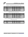
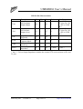
1
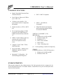
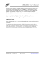
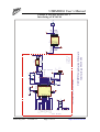
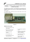
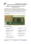
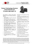
USBMOD4 User’s Manual
USBMOD4 - USB Plug and Play Parallel 8-Bit FIFO
Development Module (Second Generation)
The USBMOD4 shown in Diagram 1, is a second generation, low-cost integrated module
for transferring data to / from a peripheral and a host PC at up to 8 Million bits (1
Megabyte) per second. Based on the FTDI FT245BM USB FIFO – Fast Parallel Data
Transfer IC, it’s simple FIFO-like design makes it easy to interface to a CPU (MCU)
either by mapping the device into the memory / I/O map of the CPU, using DMA or
controlling the device via I/O ports.
The USBMOD4 offers a complete plug and play solution making it ideal for rapid
prototyping and development.
Diagram 1
MODULE FEATURES
•
•
•
•
•
Single module High-Speed USB
UART solution
•
No external passive components
required
Based on the FTDI FT245BM
USB FIFO – Fast Parallel Data
Transfer IC
•
Module powered from USB bus
in addition to supplying up to
460mA for user application
Integrated Type-B USB
Connector
•
32-pin Dual In-Line Package
(Ideal for prototyping)
•
Fits into a standard 32-pin
600mil IC Socket
On-board 6MHz Crystal
External EEPROM for USB
enumeration data
Ravar Pty Ltd
Version 1.0
Page 1 of 15
http://www.ravar.net
USBMOD4 User’s Manual
FT245BM IC FEATURES
•
Single Chip Multi-Function Data
Transfer Solution
•
Send / Receive Data over USB at
up to 1 Mb / Sec
•
384 byte receive buffer / 128
byte transmit buffer for high data
throughput
•
Simple interface to CPU or MCU
bus
•
No in-depth knowledge of USB
required as all USB Protocol is
handled automatically within the
I.C
•
FTDI’s Virtual COM port drivers
eliminate the need for USB
driver development in most
cases.
•
Compact 32 pin (7mm x 7mm)
MQFP package
•
UHCI / OHCI Compliant
•
USB 1.1 and USB 2.0
Compatible
•
USB VID, PID, Serial Number
and Product Description Strings
in external E2PROM.
VIRTUAL COM PORT (VCP)
DRIVERS for
• Windows 98, 98 SE and ME
• Windows 2000 / XP
• Windows CE **
• MAC OS-8 and OS9
• MAC OS-X
• Linux 2.40 and greater
[** = In the planning or under development]
•
Integrated 6Mhz – 48Mhz Clock
Multiplier aids FCC and CE
compliance
•
Integrated 3.3v Regulator – No
External Regulator Required
FTD2XX
(USB Direct Drivers + DLL S/W Interface)
• Windows 98, 98 SE and ME
• Windows 2000 / XP
ENHANCEMENTS
This section summarises the enhancements of the 2nd generation device compared to its
FT8U245AM predecessor. For further details, consult the device pin-out description and
functional descriptions.
Ravar Pty Ltd
Version 1.0
Page 2 of 15
http://www.ravar.net
USBMOD4 User’s Manual
• Integrated Power-On-Reset (POR)
Circuit
The device now incorporates an internal
POR function. The existing RESET# pin
(RSTI on the module) is maintained in
order to allow external logic to reset the
device where required, however for
many applications this pin can now be
either left N/C or hard wired to VCC
(+V on the module). In addition, a new
reset output pin (RSTO# or RSTO on the
module) is provided in order to allow the
new POR circuit to provide a stable reset
to external MCU and other devices.
RSTO# was the TEST pin on the
previous generation of devices.
• Integrated RCCLK Circuit
In the previous devices, an external RC
circuit was required to ensure that the
oscillator and clock multiplier PLL
frequency was stable prior to enabling
the clock internal to the device. This
circuit is now embedded on-chip – the
pin assigned to this function is now
designated as the TEST pin and should
be tied to GND for normal operation.
• Integrated Level Converter on FIFO
interface and control signals
The previous devices would drive the
FIFO and control signals at 5v CMOS
logic levels. The new device has a
separate VCC-IO (VIO on the module)
pin allowing the device to directly
interface to 3.3v and other logic families
without the need for external level
converter I.C.'s
• Power Management control for USB
Bus Powered, high current devices
A new PWREN# signal (/PEN on the
module) which can be used to directly
drive a transistor or P-Channel MOSFET
in applications where power switching
of external circuitry is required. A new
EEPROM based option makes the
Ravar Pty Ltd
Version 1.0
device pull gently down its FIFO
interface lines when the power is shut
off (PWREN# is High). In this mode,
any residual voltage on external circuitry
is bled to GND when power is removed
thus ensuring that external circuitry
controlled by PWREN# resets reliably
when power is restored. PWREN# can
also be used be external circuitry to
determine when USB is in suspend mode
(PWREN# goes high).
• Lower Suspend Current
Integration of RCCLK within the device
and internal design improvements reduce
the suspend current of the FT245BM to
under 200uA (excluding the 1.5k pull-up
on USBDP) in USB suspend mode. This
allows greater margin for peripherals to
meet the USB Suspend current limit of
500uA.
• Support for USB Isocronous
Transfers
Whilst USB Bulk transfer is usually the
best choice for data transfer, the
scheduling time of the data is not
guaranteed. For applications where
scheduling latency takes priority over
data integrity such as transferring audio
and low bandwidth video data, the new
device now offers an option of USB
Isocronous transfer via an option bit in
the EEPROM.
• Programmable FIFO TX Buffer
Timeout
In the previous device, the TX buffer
timeout used to flush remaining data
from the receive buffer was fixed at
16ms timeout. This timeout is now
programmable over USB in 1ms
increments from 1ms to 255ms thus
allowing the device to be better
optimised for protocols requiring faster
response times from short data packets.
Page 3 of 15
http://www.ravar.net
USBMOD4 User’s Manual
• Send Immediate / Wakeup (SI/WU)
signal
The new Send Immediate / WakeUp
signal combines the two functions on a
single pin. If USB is in suspend mode
(and remote wakeup is enabled in the
EEPROM), strobing this pin low will
cause the device to request a resume
from suspend (WakeUp) on the USB
Bus. Normally, this can be used to wake
up the Host PC. During normal
operation, if this pin is strobed low any
data in the device RX buffer will be sent
out over USB on the next Bulk-IN
request from the drivers regardless of the
packet size. This can be used to optimize
USB transfer speed for some
applications.
• Relaxed VCC Decoupling
The 2nd generation devices now
incorporate a level of on-chip VCC
decoupling. Though this does not
eliminate the need for external
decoupling capacitors, it significantly
improves the ease of PCB design
requirements to meet FCC, CE and other
EMI related specifications.
• Bit Bang Mode
The 2nd generation device has a new
option referred to as “Bit Bang ” mode.
In Bit Bang mode, the eight FIFO data
lines can be switched between FIFO
interface mode and an 8-bit Parallel IO
port. Data packets can be sent to the
device and they will be sequentially sent
to the interface at a rate controlled by an
internal timer (equivalent to the prescaler
of the FT232BM device). As well as
allowing the device to be used standalone as a general-purpose IO controller
for example controlling lights, relays and
switches, some other interesting
possibilities exist. For instance, it may
be possible to connect the device to an
SRAM configurable FPGA as supplied
by vendors such as Altera and Xilinx.
The FPGA device would normally be
un-configured (i.e. have no defined
function) at power-up. Application
software on the PC could use Bit Bang
Mode to download configuration data to
the FPGA, which would define its
hardware function, then after the FPGA
device is configured the FT245BM can
switch back into FIFO interface mode to
allow the programmed FPGA device to
communicate with the PC over USB.
This approach allows a customer to
create a “generic ” USB peripheral who
’s hardware function can be defined
under control of the application
software. The FPGA based hardware can
be easily upgraded or totally changed
simply by changing the FPGA
configuration data file. Application
notes, software and development
modules for this application area will be
available from FTDI and other 3rd
parties.
For further information regarding the FTDI FT245BM USB FIFO – Fast Parallel
Data Transfer IC please refer to the FT245BM Datasheet. This datasheet can be found
on the Ravar website at http://www.ravar.net
As mentioned above in module features, the USBMOD4 is in a 32-pin Dual In-Line
Package. This allows the module to fit into a standard 32-pin 600mil IC Socket which
makes the module ideal for prototyping and development work. Shown in Diagram 2
below is the pin out for the USBMOD4.
Ravar Pty Ltd
Version 1.0
Page 4 of 15
http://www.ravar.net
USBMOD4 User’s Manual
USBMOD4 PINOUT
PIN
1
PIN
32
2
31
3
30
4
29
5
28
6
27
7
26
8
25
9
24
10
23
11
22
12
21
13
20
14
19
15
18
16
17
DIAGRAM 2
On the following page is the pin out table showing what the various pins are on the
module.
Ravar Pty Ltd
Version 1.0
Page 5 of 15
http://www.ravar.net
USBMOD4 User’s Manual
USBMOD4 PINOUT TABLE
PIN
#
1
2
3
4
5
6
7
8
SIGNAL
TYPE
DESCRIPTION
G
GND
B+
+V
ECS
ECLK
EDAT
RSTI
PWR
PWR
PWR
PWR
I/O
I/O
OUT
IN
9
EP
IN
10
RSTO
OUT
11
3V3
OUT
12
VIO
PWR
13
14
+V
/PEN
PWR
OUT
Device – Ground Supply Pin
Device – Ground Supply Pin
USB Bus Power
Device - +4.4 volt to +5.25 volt Power Supply Pin
EEPROM – Chip Select
EEPROM – Clock
EEPROM – Data I/O
Can be used by external device to reset chip. If not
required tie to VCC
Enumeration Power connect to RSTO for bus powered
operation or 3V3 to instruct PC to connect to device
Output of the internal Reset Generator. Stays high
impedance for ~2ms after VCC >3.5v and the internal
clock starts up, then clamps it ’s output to the 3.3v output
of the internal regulator. Taking RESET# low will also
force RSTOUT# to go high impedance. RSTOUT# is
NOT affected by a USB Bus Reset.
3.3 volt Output from the integrated L.D.O. regulator. This
pin should be decoupled to GND using a 33nF ceramic
capacitor in close proximity to the device pin. Its prime
purpose is to provide the internal 3.3v supply to the USB
transceiver cell and the RSTO pin. A small amount of
current (<=5mA) can be drawn from this pin to power
external 3.3v logic if required.
+3.0 volt to +5.25 volt VCC to the FIFO interface pins
10..12,14..16 and 18..25. When interfacing with 3.3v
external logic connect VIO to the 3.3v supply of the
external logic, otherwise connect to +V to drive out at 5v
CMOS level.
Device - +4.4 volt to +5.25 volt Power Supply Pin
Goes Low after the device is configured via USB, then
high during USB suspend. Can be used to control power
to external logic using a P-Channel Logic Level MOSFET
switch. Enable the Interface Pull-Down Option in
EEPROM when using the /PEN pin in this way.
Ravar Pty Ltd
Version 1.0
Page 6 of 15
http://www.ravar.net
USBMOD4 User’s Manual
USBMOD4 PINOUT TABLE Continued
PIN
#
15
SIGNAL
TYPE
DESCRIPTION
SI/W
IN
16
17
GND
/RXF
PWR
OUT
18
/TXE
OUT
19
WR
IN
20
/RD
IN
21
22
23
24
25
26
27
28
29
30
31
32
D7
D6
D5
D4
D3
D2
D1
D0
GND
DD+
G
I/O
I/O
I/O
I/O
I/O
I/O
I/O
I/O
PWR
I/O
I/O
PWR
The Send Immediate /WakeUp signal combines two
functions on a single pin. If USB is in suspend mode
(/PEN=1) and remote wakeup is enabled in the EEPROM,
strobing this pin low will cause the device to request a
resume on the USB Bus. Normally, this can be used to
wake up the Host PC. During normal operation (PEN=0),
if this pin is strobed low any data in the device RX buffer
will be sent out over USB on the next Bulk-IN request
from the drivers regardless of the pending packet size.
This can be used to optimize USB transfer speed for some
applications. Tie this pin high if not used.
Device – Ground Supply Pin
When high, do not read data from FIFO. When low, there
is data available in the FIFO, which can be read by
strobing /RD low the high again.
When high, do not write data into the FIFO. When low,
data can be written into the FIFO by strobing WR high
then low.
Writes the Data Byte on D0..D7 into the Transmit FIFO
Buffer when WR goes from high to low.
Enables Current FIFO Data Byte on D0..D7 when low.
Fetches the next FIFO Data Byte (if available) from the
Receive FIFO Buffer when /RD goes from low to high.
Bi-Directional Data Bus Bit #7
Bi-Directional Data Bus Bit #6
Bi-Directional Data Bus Bit #5
Bi-Directional Data Bus Bit #4
Bi-Directional Data Bus Bit #3
Bi-Directional Data Bus Bit #2
Bi-Directional Data Bus Bit #1
Bi-Directional Data Bus Bit #0
Device – Ground Supply Pin
USB Data Signal Minus
USB Data Signal Plus
Device – Ground Supply Pin
The following page shows the schematic for the USBMOD4.
Ravar Pty Ltd
Version 1.0
Page 7 of 15
http://www.ravar.net
Version 1.0
Page 8 of 15
29
32
2
16
1
4
13
20
19
21
23
22
25
24
27
26
28
8
C2
100nF
10nF
C6
+
C4
100nF
VCC
16
15
25
24
23
22
21
20
19
18
31
4
/RD
WR
D0
D1
D2
D3
D4
D5
D6
D7
TEST
/RST
VCC
GND
GND
AGND
12
13
VCCIO
3
26
30
VCC
VCC
AVCC
R4
470
USBDP
USBDM
3V3OUT
RSTOUT#
/TXE
PWREN#
/RXF
SI/WU
EESK
EECS
EEDATA
XTIN
XTOUT
U1
FT 245B M
C3
100nF
R2
27R
1K5
C5 33nF
R6
R3
C1
10nF
30
3
7
17
15
18
14
10
11
9
31
5
20
C2
27pF
1
2
3
4
VCC
CON1
USB
+V
DATA+
DATAGND
FB1
Ferrite Bead
R5
2K2
COPYRIGHT 2002
RAVAR Pty Ltd
www. ravar.net
USB MOD4 Schematic
R1
27R
7
8
6
5
14
10
12
11
1
32
2
27
28
X1
6MHz
C3
27pF
MODULE PINS
Ravar Pty Ltd
9
17
29
VCC
6
1
2
3
4
R6
10K
CS
VCC
SK
NC
DIN
NC
DOUT GND
U2
93LC 66B
8
7
6
5
VCC
USBMOD4 User’s Manual
USBMOD4 SCHEMATIC
http://www.ravar.net
MODULE PINS
USBMOD4 User’s Manual
Driver Installation.
Your first choice when using the USBMOD4 is whether you want to use the Virtual
Com Port driver or the Direct DLL driver.
For programming simplicity the best driver is the Virtual Com Port and when installed
the USBMOD4 will appear in the System Properties / Device Manager as an USB Serial
Port (COMn) as follows.
The Com Port number will vary depending on the number of existing Com Ports on your
computer and the number of USBMOD4’s connected to your system.
To install the Virtual Com Port drivers, download the driver from our website or the
ftdichip.com website and unzip the files to a local directory. Then connect the
USBMOD4 and windows will automatically ask for the driver. Select to specify a
location and browse to the directory where you have unzipped the files. (Use the Non
Plug & Play driver for the USBMOD to avoid a delay identifying)
Ravar Pty Ltd
Version 1.0
Page 9 of 15
http://www.ravar.net
USBMOD4 User’s Manual
Once the Virtual Com Port is installed it can be programmed exactly as a regular serial
com port using the MSComm control from Visual Basic or API calls from C or other
languages. Set the com port to the same number as appears in the Device Manager, the
baud rate, stop bits, parity etc are not used as the device always runs at full speed.
The Direct DLL driver is installed in a similar manner but using the alternative download
from the website.
Programming the Direct DLL driver is by call to the DLL Library functions.
Please download the Direct DLL programmers guide from the Ravar website.
Application Notes
On the following pages there is a schematic drawing showing a sample application for the
USBMOD4.
The application shows how to interface the USBMOD4 to a micro controller. We are
using a PIC 16C84 in this application but any micro controller could be used if it has at
least 2 Input/Output ports. In this application, Port A is used for all the handshaking
while Port B is used to transmit the data between the USBMOD4 and the PIC 16C84.
Ravar Pty Ltd
Version 1.0
Page 10 of 15
http://www.ravar.net
8
Page 11 of 15
32
2
16
29
1
4
13
C2
100nF
C6
+
C4
100nF
/RD
WR
D0
D1
D2
D3
D4
D5
D6
D7
TEST
/RST
VCC
USBDP
USBDM
3V3OUT
RSTOUT#
/TXE
PWREN#
/RXF
SI/WU
EESK
EECS
EEDATA
XTIN
XTOUT
U1
FT245BM
C3
100nF
R1
27R
7
8
6
5
14
10
12
11
1
32
2
27
28
R2
27R
1K5
C5 33nF
R6
R3
C2
27pF
C1
10n F
30
3
1
2
3
4
VCC
R5
2K2
CON1
USB
+V
DATA+
DATAGND
FB1
Ferrite Bead
7
17/RXFULL
15
18/TXEMPTY
14
10
11
9
31
5
20
X1
6MHz
C3
27pF
MODULE PINS
6
1
2
3
4
8
7
6
5
COPYRIGHT 2002
RA VAR Pty L td
www. ravar.net
R6
10K
CS
VC C
SK
NC
DIN
NC
DOUT GND
U2
93LC66B
VCC
VCC
USB MOD4 Application Schematic
Interfacing a PIC16C84
The Outlined Box represents an entire USBMOD4
10nF
VCC
16
15
25
24
23
22
21
20
19
18
31
4
R4
470
3
26
30
VCC
VCC
AVCC
12
D0 28
D1 27
D2 26
D3 25
D4 24
D5 23
D6 22
D7 21
/RD 20
WR 19
MODULE PINS
13
VCCIO
Version 1.0
GND
GND
AGND
Ravar Pty Ltd
9
17
29
VCC
D0
D1
D2
D3
/TXEMPTY
/RXFULL
1
2
3
4
5
6
7
8
9
U3
PIC16C84
RA2
RA3
RTC/A4
MCLR
VSS
INT/B0
RB1
RB2
RB3
RA1
RA0
OSC1
OSC2
VDD
RB7
RB6
RB5
RB4
18
17
16
15
14
13
12
11
10
D7
D6
D5
D4
/RD
WR
VCC
X1
4Mhz
USBMOD4 User’s Manual
SAMPLE APPLICATION No. 1
Interfacing a PIC16C84
http://www.ravar.net
USBMOD4 User’s Manual
Absolute Maximum Ratings
Storage Temperature ……………………………………………..
Ambient Temperature ( Power Applied )………………………...
VCC Supply Voltage …………………………………………….
DC Input Voltage - Inputs ……………………………………….
DC Input Voltage - High Impedance Bidirectionals …………….
DC Output Current – Outputs ……………………………………
DC Output Current – Low Impedance Bidirectionals …………...
Power Dissipation ……………………………………………….
Electrostatic Discharge Voltage …………………………………
Latch Up Current (Vi < 0 or Vi > Vcc) …………………………
-65°C to + 150°C
0°C to + 70°C
-0.5v to +6.00v
-0.5v to VCC + 0.5v
-0.5v to VCC + 0.5v
24mA
24mA
500mW
+/- 2000V
100mA
DC Characteristics (Ambient Temperature = 0°C .. 70°C)
Operating Voltage and Current
Parameter
Description
+V Operating Supply
Voltage
VIO Operating
Supply Voltage
Operating Supply
Current
Operating Supply
Current
Vcc1
Vcc2
Icc1
Icc2
Min
Typ
Max
Units
Conditions
4.4
5.0
5.25
V
3.0
-
5.25
V
-
25
-
mA
Normal Operation
-
100
200
uA
USB Suspend
FIFO Data / Control Bus I/O Pin Characteristics (VIO = 5V)
Parameter
Voh
Vol
Vin
VHys
Description
Min Typ Max Units
Conditions
Output Voltage High
4.4
4.9
V
I source = 2 mA
Output Voltage Low
0.1
0.7
V
I sink = 4 mA
Input Switching
1.1
1.5
1.8
V
* Note 1
Threshold
Input Switching
200
mV
Hysteresis
* Note 1 – Inputs have an internal 200kΩ pull-up resistor to VIO
Ravar Pty Ltd
Version 1.0
Page 12 of 15
http://www.ravar.net
USBMOD4 User’s Manual
FIFO Data / Control Bus I/O Pin Characteristics (VIO = 3.3V)
Parameter
Voh
Vol
Vin
VHys
Description
Min Typ Max Units Conditions
Output Voltage High
2.7
3.2
V
I source = 2 mA
Output Voltage Low
0.1
0.7
V
I sink = 4 mA
Input Switching
1.0
1.4
1.8
V
* Note 1
Threshold
Input Switching
200
mV
Hysteresis
* Note 1 – Inputs have an internal 200kΩ pull-up resistor to VIO
RSTI, ECS, EDAT I/O Pin Characteristics
Parameter
Voh
Vol
Vin
VHys
Description
Output Voltage High
Output Voltage Low
Input Switching
Threshold
Input Switching
Hysteresis
Min
4.4
0.1
Typ
-
Max
4.9
0.7
Units
V
V
Conditions
I source = 2 mA
I sink = 4 mA
1.1
1.5
1.8
V
* Note 2
200
mV
* Note 2 – ECS and EDAT pins have an internal 200kΩ pull-up resistor to +V
RSTO Pin Characteristics
Parameter
Voh
Iol
Ravar Pty Ltd
Description
Output Voltage High
Leakage Current TriState
Version 1.0
Min
3.0
Typ
-
Max
3.6
Units
V
-
-
5
uA
Page 13 of 15
Conditions
I source = 2 mA
http://www.ravar.net
USBMOD4 User’s Manual
USB I/O Pin Characteristics
Parameter
Description
Min
Typ
Max
Units
UVoh
I/O Pins Static
Output (High)
4.4
-
4.9
V
UVol
I/O Pin Static
Output (Low)
0.1
-
0.7
V
0.8
2.0
V
0.8
2.5
V
UVse
UCom
UVDif
UDrvZ
Single Ended RX
Threshold
Differential
Common Mode
Differential Input
Sensitivity
Driver Output
Impedance
0.2
29
Conditions
Rl = 1.5kÙ to
3V3Out (D+) Rl
= 15kÙ to GND
(D+)
Rl = 1.5kÙ to
3V3Out (D+) Rl
= 15kÙ to GND
(D+)
V
44
Ù (ohm)
* Note 3
* Note 3 – Driver Output Impedance includes the external 27Ù series resistors on D+ and
D- pins.
Ravar Pty Ltd
Version 1.0
Page 14 of 15
http://www.ravar.net
USBMOD4 User’s Manual
Technical Support and Further Information
For any questions relating to the USBMOD4 please contact us by Email, Fax or Phone.
email: [email protected]
Fax: +61 755 914364
Ph: +61 755 325688
Ravar Pty Ltd
5G Jackman Center
Jackman Street, Southport
Queensland 4215
Australia
Ravar Pty Ltd
PO Box 2514
Southport
Queensland 4215
Australia
Product Use Limitations, Warranty and Quality Statement.
The USBMOD4 should not be used in any situation where it’s failure or failure of the PC
or software controlling it could cause human injury or severe damage to equipment.
This device is not designed for or intended to be used in any life critical application.
The USBMOD4 is warranted to be free from manufacture defects for a period of 12
months from the date purchase.
Subjecting the device to conditions beyond the Absolute Maximum Ratings listed above
will invalidate this warranty.
The USBMOD4 is a static sensitive device, anti static procedures should be used in the
handling of this device.
All USBMOD4 units are extensively tested at time of manufacture to be free of defects.
Ravar is committed to providing products of the highest quality. Should you experience
any product quality issues with this product please contact our quality assurance manager
at the above address.
Disclaimer.
This product and its documentation are provided as-is and no warranty is made or implied
as to their suitability for any particular purpose.
Ravar Pty Ltd will not accept any claim for damages arising from the use of this product
or documentation.
This document provides information on our products and all efforts are made to ensure
the accuracy of the information contained within. The specifications of the product are
subject to change and continual improvement.
Ravar Pty Ltd
Version 1.0
Page 15 of 15
http://www.ravar.net