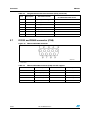
1
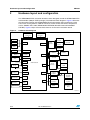
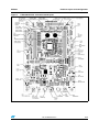
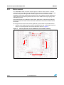
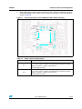
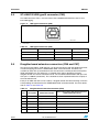
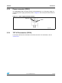
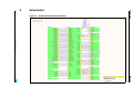
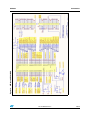
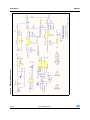
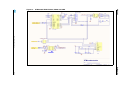
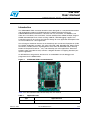
UM1567
User manual
STM32303C-EVAL evaluation board
Introduction
The STM32303C-EVAL evaluation board has been designed as a complete demonstration
and development platform for STMicroelectronic's ARM cortex-M4 core-based
STM32F303VCT6 microcontrollers. It features two I2Cs, three SPIs, five USARTs, one
CAN, four 12-bit ADCs, two 12-bit DACs, internal 40-KByte Data SRAM, 8-KByte Program
SRAM and 256-KByte Flash, Touch sensing, USB FS, JTAG debugging support. This
evaluation board can be used as the reference design for user application development but
it is not considered as a final application.
The full range of hardware features on the board help you to evaluate all peripherals (USB
FS, USART, Audio DAC and ADC, TFT color LCD, IrDA, LDR, MicroSD card, Motor control
connectors, Humidity Sensor, High Brightness LED, CAN, IR, EEPROM, Touch Sensing
Buttons & Temperature Sensor… etc.) and to develop your own applications. Extension
headers make it possible to easily connect a daughter board or a wrapping board for your
specific application.
An ST-LINK/V2 is integrated on the board as an embedded in-circuit debugger and
programmer for the STM32 MCU.
Figure 1.
STM32303C-EVAL evaluation board
Table 1 lists the evaluation tools concerned by this user manual.
Table 1.
Applicable tools
Type
Evaluation tools
February 2013
Applicable tools
STM32303C-EVAL
Doc ID 023581 Rev 2
1/58
www.st.com
Contents
UM1567
Contents
1
2
3
Overview . . . . . . . . . . . . . . . . . . . . . . . . . . . . . . . . . . . . . . . . . . . . . . . . . . 6
1.1
Features . . . . . . . . . . . . . . . . . . . . . . . . . . . . . . . . . . . . . . . . . . . . . . . . . . . 6
1.2
Demonstration software . . . . . . . . . . . . . . . . . . . . . . . . . . . . . . . . . . . . . . . 6
1.3
Order code . . . . . . . . . . . . . . . . . . . . . . . . . . . . . . . . . . . . . . . . . . . . . . . . . 6
1.4
Delivery recommendations . . . . . . . . . . . . . . . . . . . . . . . . . . . . . . . . . . . . . 7
Hardware layout and configuration . . . . . . . . . . . . . . . . . . . . . . . . . . . . . 8
2.1
Development and debug support . . . . . . . . . . . . . . . . . . . . . . . . . . . . . . . 10
2.2
Power supply . . . . . . . . . . . . . . . . . . . . . . . . . . . . . . . . . . . . . . . . . . . . . . 11
2.3
Clock source . . . . . . . . . . . . . . . . . . . . . . . . . . . . . . . . . . . . . . . . . . . . . . . 13
2.4
Reset source . . . . . . . . . . . . . . . . . . . . . . . . . . . . . . . . . . . . . . . . . . . . . . 14
2.5
Boot option . . . . . . . . . . . . . . . . . . . . . . . . . . . . . . . . . . . . . . . . . . . . . . . . 14
2.6
Audio . . . . . . . . . . . . . . . . . . . . . . . . . . . . . . . . . . . . . . . . . . . . . . . . . . . . 15
2.7
USB . . . . . . . . . . . . . . . . . . . . . . . . . . . . . . . . . . . . . . . . . . . . . . . . . . . . . 16
2.8
RS232, RS-485 and IrDA . . . . . . . . . . . . . . . . . . . . . . . . . . . . . . . . . . . . . 16
2.9
Touch-sensing buttons . . . . . . . . . . . . . . . . . . . . . . . . . . . . . . . . . . . . . . . 17
2.10
MicroSD card . . . . . . . . . . . . . . . . . . . . . . . . . . . . . . . . . . . . . . . . . . . . . . 18
2.11
Serial EEPROM . . . . . . . . . . . . . . . . . . . . . . . . . . . . . . . . . . . . . . . . . . . . 18
2.12
RF EEPROM . . . . . . . . . . . . . . . . . . . . . . . . . . . . . . . . . . . . . . . . . . . . . . 18
2.13
EEPROM . . . . . . . . . . . . . . . . . . . . . . . . . . . . . . . . . . . . . . . . . . . . . . . . . 18
2.14
CAN . . . . . . . . . . . . . . . . . . . . . . . . . . . . . . . . . . . . . . . . . . . . . . . . . . . . . 19
2.15
IR LED and IR receiver . . . . . . . . . . . . . . . . . . . . . . . . . . . . . . . . . . . . . . 19
2.16
High brightness LED . . . . . . . . . . . . . . . . . . . . . . . . . . . . . . . . . . . . . . . . 19
2.17
Humidity sensor . . . . . . . . . . . . . . . . . . . . . . . . . . . . . . . . . . . . . . . . . . . . 19
2.18
Comparator . . . . . . . . . . . . . . . . . . . . . . . . . . . . . . . . . . . . . . . . . . . . . . . 20
2.19
Temperature sensor . . . . . . . . . . . . . . . . . . . . . . . . . . . . . . . . . . . . . . . . . 20
2.20
Display and input devices . . . . . . . . . . . . . . . . . . . . . . . . . . . . . . . . . . . . . 21
2.21
Motor control . . . . . . . . . . . . . . . . . . . . . . . . . . . . . . . . . . . . . . . . . . . . . . 22
Connector . . . . . . . . . . . . . . . . . . . . . . . . . . . . . . . . . . . . . . . . . . . . . . . . 26
3.1
2/58
RF EEPROM daughter board connector (CN1) . . . . . . . . . . . . . . . . . . . . 26
Doc ID 023581 Rev 2
UM1567
4
Contents
3.2
Motor control connector (CN2) . . . . . . . . . . . . . . . . . . . . . . . . . . . . . . . . . 27
3.3
CAN D-type 9-pin male connector (CN3) . . . . . . . . . . . . . . . . . . . . . . . . . 28
3.4
Motor control connector (CN4) . . . . . . . . . . . . . . . . . . . . . . . . . . . . . . . . . 29
3.5
ST-LINK/V2 USB type-B connector (CN5) . . . . . . . . . . . . . . . . . . . . . . . . 30
3.6
Daughter board extension connectors (CN6 and CN7) . . . . . . . . . . . . . . 30
3.7
RS232 and RS485 connector (CN8) . . . . . . . . . . . . . . . . . . . . . . . . . . . . 34
3.8
ETM Trace debugging connector (CN9) . . . . . . . . . . . . . . . . . . . . . . . . . . 35
3.9
JTAG/SWD connector (CN10) . . . . . . . . . . . . . . . . . . . . . . . . . . . . . . . . . 35
3.10
Audio jack (CN11) . . . . . . . . . . . . . . . . . . . . . . . . . . . . . . . . . . . . . . . . . . 36
3.11
User USB type-B connector (CN12) . . . . . . . . . . . . . . . . . . . . . . . . . . . . . 36
3.12
ST-LINK/V2 programming connector (CN13) . . . . . . . . . . . . . . . . . . . . . . 36
3.13
Power connector (CN14) . . . . . . . . . . . . . . . . . . . . . . . . . . . . . . . . . . . . . 37
3.14
TFT LCD connector (CN15) . . . . . . . . . . . . . . . . . . . . . . . . . . . . . . . . . . . 37
3.15
MicroSD connector (CN16) . . . . . . . . . . . . . . . . . . . . . . . . . . . . . . . . . . . 38
Schematics . . . . . . . . . . . . . . . . . . . . . . . . . . . . . . . . . . . . . . . . . . . . . . . 39
Appendix A STM32303C-EVAL I/O assignment . . . . . . . . . . . . . . . . . . . . . . . . . . 53
Appendix B Mechanical dimensions. . . . . . . . . . . . . . . . . . . . . . . . . . . . . . . . . . . 56
Revision history . . . . . . . . . . . . . . . . . . . . . . . . . . . . . . . . . . . . . . . . . . . . . . . . . . . . 57
Doc ID 023581 Rev 2
3/58
List of tables
UM1567
List of tables
Table 1.
Table 2.
Table 3.
Table 4.
Table 5.
Table 6.
Table 7.
Table 8.
Table 9.
Table 10.
Table 11.
Table 12.
Table 13.
Table 14.
Table 15.
Table 16.
Table 17.
Table 18.
Table 19.
Table 20.
Table 21.
Table 22.
Table 23.
Table 24.
Table 25.
Table 26.
Table 27.
Table 28.
Table 29.
Table 30.
Table 31.
Table 32.
Table 33.
Table 34.
Table 35.
Table 36.
4/58
Applicable tools. . . . . . . . . . . . . . . . . . . . . . . . . . . . . . . . . . . . . . . . . . . . . . . . . . . . . . . . . . . 1
Third-party support of ST-LINK/V2 . . . . . . . . . . . . . . . . . . . . . . . . . . . . . . . . . . . . . . . . . . . 10
Power supply jumper settings . . . . . . . . . . . . . . . . . . . . . . . . . . . . . . . . . . . . . . . . . . . . . . . 11
Power mode related jumpers . . . . . . . . . . . . . . . . . . . . . . . . . . . . . . . . . . . . . . . . . . . . . . . 12
Low voltage limitation . . . . . . . . . . . . . . . . . . . . . . . . . . . . . . . . . . . . . . . . . . . . . . . . . . . . . 13
32 kHz crystal X1 related solder bridges . . . . . . . . . . . . . . . . . . . . . . . . . . . . . . . . . . . . . . 13
8 MHz crystal X2 related solder bridges . . . . . . . . . . . . . . . . . . . . . . . . . . . . . . . . . . . . . . . 14
Boot-related switch . . . . . . . . . . . . . . . . . . . . . . . . . . . . . . . . . . . . . . . . . . . . . . . . . . . . . . . 14
Boot0-related jumper . . . . . . . . . . . . . . . . . . . . . . . . . . . . . . . . . . . . . . . . . . . . . . . . . . . . . 15
Audio-related jumpers. . . . . . . . . . . . . . . . . . . . . . . . . . . . . . . . . . . . . . . . . . . . . . . . . . . . . 15
RS232, RS485 and IrDA related jumpers . . . . . . . . . . . . . . . . . . . . . . . . . . . . . . . . . . . . . . 16
RS485 related solder bridges . . . . . . . . . . . . . . . . . . . . . . . . . . . . . . . . . . . . . . . . . . . . . . . 17
Touch-sensing button related solder bridges . . . . . . . . . . . . . . . . . . . . . . . . . . . . . . . . . . . 17
EEPROM Related Jumpers . . . . . . . . . . . . . . . . . . . . . . . . . . . . . . . . . . . . . . . . . . . . . . . . 18
CAN related jumpers . . . . . . . . . . . . . . . . . . . . . . . . . . . . . . . . . . . . . . . . . . . . . . . . . . . . . 19
Humidity sensor related jumper . . . . . . . . . . . . . . . . . . . . . . . . . . . . . . . . . . . . . . . . . . . . . 20
Temperature sensor related jumpers . . . . . . . . . . . . . . . . . . . . . . . . . . . . . . . . . . . . . . . . . 20
LCD modules . . . . . . . . . . . . . . . . . . . . . . . . . . . . . . . . . . . . . . . . . . . . . . . . . . . . . . . . . . . 21
Motor control related jumpers . . . . . . . . . . . . . . . . . . . . . . . . . . . . . . . . . . . . . . . . . . . . . . . 23
Motor control related switches and solder bridges in OAM position . . . . . . . . . . . . . . . . . . 24
Motor control related switches and solder bridges in PGM position . . . . . . . . . . . . . . . . . . 25
RF EEPROM daughter board connector (CN1) . . . . . . . . . . . . . . . . . . . . . . . . . . . . . . . . . 26
Motor control 1 connector (CN2) . . . . . . . . . . . . . . . . . . . . . . . . . . . . . . . . . . . . . . . . . . . . 27
CAN D-type 9-pin male connector (CN3) . . . . . . . . . . . . . . . . . . . . . . . . . . . . . . . . . . . . . . 28
Motor control 2 connector (CN4) . . . . . . . . . . . . . . . . . . . . . . . . . . . . . . . . . . . . . . . . . . . . 29
USB type-B connector (CN5) . . . . . . . . . . . . . . . . . . . . . . . . . . . . . . . . . . . . . . . . . . . . . . . 30
Daughter board extension connector (CN6) . . . . . . . . . . . . . . . . . . . . . . . . . . . . . . . . . . . . 30
Daughter board extension connector (CN7) . . . . . . . . . . . . . . . . . . . . . . . . . . . . . . . . . . . . 32
RS232 and RS485 connector (CN8) with ISP support . . . . . . . . . . . . . . . . . . . . . . . . . . . . 34
ETM trace debugging connector (CN9) . . . . . . . . . . . . . . . . . . . . . . . . . . . . . . . . . . . . . . . 35
JTAG/SWD debugging connector CN10 . . . . . . . . . . . . . . . . . . . . . . . . . . . . . . . . . . . . . . 36
USB type-B connector (CN12) . . . . . . . . . . . . . . . . . . . . . . . . . . . . . . . . . . . . . . . . . . . . . . 36
MicroSD connector (CN16). . . . . . . . . . . . . . . . . . . . . . . . . . . . . . . . . . . . . . . . . . . . . . . . . 38
STM32303C-EVAL I/O assignment . . . . . . . . . . . . . . . . . . . . . . . . . . . . . . . . . . . . . . . . . . 53
Mechanical dimensions . . . . . . . . . . . . . . . . . . . . . . . . . . . . . . . . . . . . . . . . . . . . . . . . . . . 56
Document revision history . . . . . . . . . . . . . . . . . . . . . . . . . . . . . . . . . . . . . . . . . . . . . . . . . 57
Doc ID 023581 Rev 2
UM1567
List of figures
List of figures
Figure 1.
Figure 2.
Figure 3.
Figure 4.
Figure 5.
Figure 6.
Figure 7.
Figure 8.
Figure 9.
Figure 10.
Figure 11.
Figure 12.
Figure 13.
Figure 14.
Figure 15.
Figure 16.
Figure 17.
Figure 18.
Figure 19.
Figure 20.
Figure 21.
Figure 22.
Figure 23.
Figure 24.
Figure 25.
Figure 26.
Figure 27.
Figure 28.
Figure 29.
Figure 30.
Figure 31.
Figure 32.
STM32303C-EVAL evaluation board . . . . . . . . . . . . . . . . . . . . . . . . . . . . . . . . . . . . . . . . . . 1
Hardware block diagram . . . . . . . . . . . . . . . . . . . . . . . . . . . . . . . . . . . . . . . . . . . . . . . . . . . . 8
STM32303C-EVAL evaluation board layout . . . . . . . . . . . . . . . . . . . . . . . . . . . . . . . . . . . . . 9
STM32303C-EVAL comparator features . . . . . . . . . . . . . . . . . . . . . . . . . . . . . . . . . . . . . . 20
Resistor positions on the PCB board: even number removing . . . . . . . . . . . . . . . . . . . . . . 22
Resistor positions on the PCB board: odd number mounting . . . . . . . . . . . . . . . . . . . . . . . 23
RF EEPROM daughter board connector (CN1) . . . . . . . . . . . . . . . . . . . . . . . . . . . . . . . . . 26
Motor control 1 connector (CN2) . . . . . . . . . . . . . . . . . . . . . . . . . . . . . . . . . . . . . . . . . . . . 27
CAN D-type 9-pin male connector (CN3) . . . . . . . . . . . . . . . . . . . . . . . . . . . . . . . . . . . . . . 28
Motor control 2 connector (CN4) . . . . . . . . . . . . . . . . . . . . . . . . . . . . . . . . . . . . . . . . . . . . 29
USB type-B connector (CN5) . . . . . . . . . . . . . . . . . . . . . . . . . . . . . . . . . . . . . . . . . . . . . . . 30
RS232 and RS485 connector . . . . . . . . . . . . . . . . . . . . . . . . . . . . . . . . . . . . . . . . . . . . . . . 34
ETM Trace debugging connector (CN9) . . . . . . . . . . . . . . . . . . . . . . . . . . . . . . . . . . . . . . . 35
JTAG/SWD debugging connector (CN10) . . . . . . . . . . . . . . . . . . . . . . . . . . . . . . . . . . . . . 35
USB type-B connector (CN12) . . . . . . . . . . . . . . . . . . . . . . . . . . . . . . . . . . . . . . . . . . . . . . 36
Power supply connector (CN14) . . . . . . . . . . . . . . . . . . . . . . . . . . . . . . . . . . . . . . . . . . . . . 37
MicroSD connector (CN16). . . . . . . . . . . . . . . . . . . . . . . . . . . . . . . . . . . . . . . . . . . . . . . . . 38
STM32330C-EVAL board (MB1019) . . . . . . . . . . . . . . . . . . . . . . . . . . . . . . . . . . . . . . . . . 39
STM32330C-EVAL MCU . . . . . . . . . . . . . . . . . . . . . . . . . . . . . . . . . . . . . . . . . . . . . . . . . . 40
STM32330C-EVAL Power . . . . . . . . . . . . . . . . . . . . . . . . . . . . . . . . . . . . . . . . . . . . . . . . . 41
STM32330C-EVAL RS232, RS485 and IrDA . . . . . . . . . . . . . . . . . . . . . . . . . . . . . . . . . . . 42
STM32330C-EVAL Audio . . . . . . . . . . . . . . . . . . . . . . . . . . . . . . . . . . . . . . . . . . . . . . . . . 43
STM32330C-EVAL Motor control . . . . . . . . . . . . . . . . . . . . . . . . . . . . . . . . . . . . . . . . . . . . 44
STM32330C-EVAL CAN, IR, High-brightness LED and Humidity sensor . . . . . . . . . . . . . 45
STM32330C-EVAL LCD, SDCard and Flash . . . . . . . . . . . . . . . . . . . . . . . . . . . . . . . . . . . 46
STM32330C-EVAL I2C peripherals . . . . . . . . . . . . . . . . . . . . . . . . . . . . . . . . . . . . . . . . . . 47
STM32330C-EVAL peripherals . . . . . . . . . . . . . . . . . . . . . . . . . . . . . . . . . . . . . . . . . . . . . 48
STM32330C-EVAL ST-LINK (JTAG only) . . . . . . . . . . . . . . . . . . . . . . . . . . . . . . . . . . . . . 49
STM32330C-EVAL JTAG and Trace . . . . . . . . . . . . . . . . . . . . . . . . . . . . . . . . . . . . . . . . . 50
TM32330C-EVAL touch sensing . . . . . . . . . . . . . . . . . . . . . . . . . . . . . . . . . . . . . . . . . . . . 51
Color LCD daughter board (MB895) . . . . . . . . . . . . . . . . . . . . . . . . . . . . . . . . . . . . . . . . . . 52
Mechanical dimensions . . . . . . . . . . . . . . . . . . . . . . . . . . . . . . . . . . . . . . . . . . . . . . . . . . . 56
Doc ID 023581 Rev 2
5/58
Overview
UM1567
1
Overview
1.1
Features
1.2
■
Four 5 V power supply options: Power jack, ST-LINK/V2 USB connector, User USB
connector or daughter board
■
I2S Audio DAC, stereo audio jack which supports headset with microphone
■
2-Gbyte or more SPI interface MicroSD card
■
I2C compatible serial interface temperature sensor, EEPROM and RF EEPROM
■
RS232 and RS485 communication
■
IrDA transceiver
■
JTAG/SWD and ETM trace debug support, ST-LINK/V2 embedded
■
1-Mbit SPI serial Flash memory
■
240x320 TFT color LCD connected to the SPI interface
■
Joystick with 4-direction control and selector
■
Reset, Tamper or Key button
■
4-color user LEDs and high brightness LED
■
Humidity sensor
■
Extension connectors for daughter board or wrapping board
■
MCU voltage choice: 3.3 V or adjustable from 2.0 V to 3.6 V
■
USB FS connector
■
Touch-sensing buttons
■
RTC with backup battery
■
CAN2.0A/B compliant connection
■
Light-dependent resistor (LDR)
■
IR LED and receiver
■
Potentiometer
■
2 motor control connectors
Demonstration software
The demonstration software is preloaded in the board's Flash memory for an easy
demonstration of the device peripherals in standalone mode. For more information and to
download the latest version available, please refer to the STM32303C-EVAL demonstration
software available on www.st.com.
1.3
Order code
To order the STM32F303VCT6 evaluation board, use the STM32303C-EVAL order code.
6/58
Doc ID 023581 Rev 2
UM1567
1.4
Overview
Delivery recommendations
Before using the board for the first time, please verify that nothing was damaged during
shipment and that no components are unplugged or lost.
When the board is extracted from its plastic bag, please check that no component remains
in the bag.
The main components to verify are:
1.
The 8 MHz crystal (X2) which may have been removed from its socket by a shock.
2.
The MicroSD card which may have been ejected from the CN16 connector (right side
of the board).
3.
The dual-interface EEPROM board (ANT7-M24LR-A) which may have been unplugged
from the CN1 connector (top left corner of the board).
For all information concerning the version of the MCU used on the board, its specification
and possible related limitations, please visit the ST web site to download the relevant data
sheet and erratasheet.
Warning:
This equipment contains parts (principally an LCD), subject to
be damaged by electrostatic discharge (ESD). Before touching
the LCD or its connector (CN1 on MB895), use one of these
following ESD precautionary procedures:
Wear a ground strap. The function of such strap is to rapidly
and safely dissipate personnel static charge to the ground.
Touch the ground before all other nets or components on
board. The easiest way to proceed is to touch with a finger the
shield available on DB9 connectors (CN3 & CN8), USB
connector (CN5) or uSD card connector (CN16).
Doc ID 023581 Rev 2
7/58
Hardware layout and configuration
2
UM1567
Hardware layout and configuration
The STM32303C-EVAL evaluation board has been designed around the STM32F303VCT6
microcontroller (100-pin TQFP package). The hardware block diagram in Figure 2 illustrates
the connection between the STM32F303VCT6 microcontroller and its peripherals (color
LCD, touch sensing buttons, USB FS connector, motor control connectors, temperature
sensor, USART, IrDA, Audio, EEPROM,RF EEPROM, MicroSD card and embedded
ST-LINK). Figure 3 helps to locate these features on the actual evaluation board.
Figure 2.
Hardware block diagram
Motor Control
connector 1
Motor Control
connector 2
RS232
transceiver
Joystick
LEDs
GPIO
USART1
Voltage
translator
RS485
transceiver
Key
button
Photo-R
Touch Sensing
Buttons
High current
LEDs
IrDA
transceiver
Comparator
Embedded
ST -LINK/V2
TS
controller
JTAG & Trace
connector
Comparator
MicroSD
card
STM32F303VCT6
SPI2
TIM
Voltage
translator
TFT color
LCD
EEPROM
PWM
USB
connector
USB TypeB
connector
JTAG
PWM
Humidity
Sensor
RS232/RS485
connector
USB FS
Audio
Codec &
Amplifier
I2S
Headset Jack
Microphone
CAN driver
& Connector
CAN
IR LED &
IR receiver
IRTIM
PWM
Potentiometer
Comparator
EEPROM
I2C
RF EEPROM
connector
Temperature
Sensor
2.0V to 3.6V
adjustable
regulator
3.3V
regulator
Extension
connector for
GPIOs
MS30710V1
Note:
8/58
‘o’ = I/O shared with Motor Control.
Doc ID 023581 Rev 2
UM1567
Figure 3.
Hardware layout and configuration
STM32303C-EVAL evaluation board layout
..
Doc ID 023581 Rev 2
9/58
Hardware layout and configuration
2.1
UM1567
Development and debug support
Version 2 of ST-LINK, called ST-LINK/V2, is embedded on the board. This tool allows
program loading and debugging of the STM32 on board using a JTAG or SWD interface.
The third-party debug tools are also supported by the JTAG/SWD connector, CN10, or the
ETM Trace connector, CN9.
A specific driver needs to be installed on your PC for communication with embedded STLINK/V2.The install shield called ST-LINK_V2_USBdriver.exe is available at
www.st.com/stlinkv2.
Third-party toolchains, Atollic TrueSTUDIO, KEIL MDK-ARM, IAR EWARM and Tasking VXToolset support ST-LINK/V2 according to Table 2.
Table 2.
Third-party support of ST-LINK/V2
Toolchain
Third party
Version
Atollic
TrueSTUDIO
2.1
IAR
EWARM
6.20
Keil
MDK-ARM
4.20
TASKING
VX-toolset for ARM Cortex-M
4.0.1
The embedded ST-LINK/V2 is connected to the PC via a standard USB cable connected to
connector CN5.The bicolor LED LD8 (COM) advises on the status of the communication as
follows:
Note:
●
Slow blinking red/off: at power on before USB init
●
Fast blinking red/off: after the first correct communication between PC and ST-Link/V2
(enumeration)
●
Red LED on: when the initialization between PC and ST-LINK/V2 has been successful
●
Green LED on: after a successful target communication initialization
●
Blinking red/green: during communication with target
●
Red on: communication finished and OK
●
Orange on: communication failure
The board can be powered via CN5 (Embedded ST/LINK/V2 USB connector) even if an
external tool is connected to CN9 (ETM Trace connector) or CN10 (External JTAG & SWD
connector).
R111 needs to be removed when using ETM 4-bit function. In this case, the key button does
not work.
10/58
Doc ID 023581 Rev 2
UM1567
2.2
Hardware layout and configuration
Power supply
The STM32303C-EVAL evaluation board has been designed to be powered by 5 V DC
power supply and to be protected by PolyZen from wrong power plug-in event. The
evaluation board can be configured to use any of the four following sources of power supply:
●
5 V DC power adapter connected to CN14, the power jack on the board (Power supply
unit (PSU) on silkscreen of JP14). The external power supply is not provided with the
board.
●
5 V DC power with 500 mA limitation from CN5, the USB type B connector of STLINK/V2 (USB 5 V power source on silkscreen of JP14 ( STlk)).
●
5V DC power with 500mA limitation from CN12, the USB type B connector (USB 5V
power source on silkscreen of JP14 (USB)).
●
5V DC power from CN6 & CN7, the extension connectors for daughter board (daughter
board power source on silkscreen of JP14 (D5V)).
The power s4upply is configured by setting the related jumpers JP14, JP15, JP16 and JP17
as described in Table 3.
Table 3.
Jumper
Power supply jumper settings
Description
Setting
STlk
PSU
U5V
D5V
JP14 is used to select one of the four possible power supply resources.
For power supply from the daughter board connectors (CN6 and CN7) to
STM32303C-EVAL only, JP14 is set as shown to the right:
For power supply from USB (CN12) to STM32303C-EVAL only, JP14 is set as
shown to the right:
JP14
For power supply jack (CN14) to the STM32303C-EVAL only, JP14 is set as
shown to the right:
For power supply from USB connector of ST-LINK/V2 (CN5) to STM32303C EVAL only, JP14 is set as shown to the right (default setting):
For power supply from power supply jack (CN14) to both STM32303C -EVAL and
daughter board connected on CN6 and CN7, JP14 is set as shown to the right
(the daughter board must not have its own power supply connected):
Vbat is connected to the battery when JP16 is set as shown to the right:
JP16
Vbat is connected to VDD power when JP16 is set as shown to the right (default
setting):
Doc ID 023581 Rev 2
11/58
Hardware layout and configuration
Table 3.
UM1567
Power supply jumper settings (continued)
Jumper
Description
Setting
VDD is connected to fixed +3.3 V DC power when JP15 is set as shown to the
right (default setting):
JP15
VDD is connected to adjustable DC power from 2.0 V to 3.6 V when JP15 is set
as shown to the right:
VDDA power is connected to VDD when JP17 is set as shown to the right (default
setting):
JP17
VDDA power is connected to fixed +3.3 V DC power when JP17 is set as shown
to the right:
Note:
Though technically adjustable from 2.0 V to 3.6 V, VDD has been designed to adjust from
2.1 V to 3.5 V considering some peripheral component specifications.
LED LD8 is lit when the STM32303C-EVAL evaluation board is correctly powered by 5 V.
A total of three power modes are supported on the board, and can be configured by setting
the related jumpers JP15 and JP17 as described in Table 4 and the Note below.
●
Mode1: VDD and VDDA were connected together and powered by fixed 3.3 V.
●
Mode2: VDD and VDDA were connected together and powered by an adjustable
voltage from 2.0 V to 3.6 V.
●
Mode3: VDD is powered by an adjustable voltage from 2.0 V to 3.6 V while VDDA is
powered by fixed 3.3 V.
Table 4.
Power mode related jumpers
Power mode configuration
MCU IDD
measurement
Power mode
JP15
JP17
OK
Mode1
NOT allowed
12/58
Mode2
OK
Mode3
NOT allowed
Doc ID 023581 Rev 2
UM1567
Note:
Hardware layout and configuration
MCU IDD measurement can be done by the current meter which is mounted on JP12 when it
is open.
JP11 must be open (disconnect VDDA from all analog power VDD_ANA connected to the
analog circuit) for MCU IDD measurement.
Due to the characters of some peripheral components' specification, the low voltage
limitations related to the operating voltage of the peripherals (a component will not work
correctly when the power level is under the low voltage limitation) are shown in Table 5.
Table 5.
Low voltage limitation
Peripheral
Component
I/O name
Low voltage limitation
USB
CN12
USB
3V
CAN
CN3
CAN
3V
Temperature sensor
U1
I2C2
2.25V
Note:
When an external DC 5V power supply is used to power the STM32303C-EVAL, it needs to
be connected to CN14 after verifying the correct polarity as explained in Section 3.13.
Caution:
RISK OF EXPLOSION IF THE BATTERY IS REPLACED BY AN INCORRECT TYPE.
DISPOSE OF USED BATTERIES ACCORDING TO THE INSTRUCTIONS.
2.3
Clock source
Two clock sources are available on the STM32303C-EVAL evaluation board for
STM32F303VCT6 and RTC embedded:
●
X1, 32 kHz crystal for embedded RTC
●
X2, 8 MHz crystal with socket for the STM32F303VCT6 microcontroller; it can be
removed from the socket when an internal RC clock is used.
Table 6.
32 kHz crystal X1 related solder bridges
Solder bridge
Description
PC14 is connected to the 32 KHz crystal when SB12 is open (default setting).
SB12
PC14 is connected to the extension connector CN6 when SB12 is closed. In such
a case, R196 must be removed to avoid disturbance due to the 32 KHz quartz.
PC15 is connected to the 32 KHz crystal when SB13 is open (default setting).
SB13
PC15 is connected to the extension connector CN6 when SB13 is closed. In such
a case, R197 must be removed to avoid disturbance due to the 32 KHz quartz.
Doc ID 023581 Rev 2
13/58
Hardware layout and configuration
Table 7.
UM1567
8 MHz crystal X2 related solder bridges
Solder bridge
Description
PF0 is connected to the 8 MHz crystal when SB14 is open (default setting).
SB14
PF0 is connected to the extension connector CN7 when SB14 is closed. In such a
case, C51 and X2 must be removed to avoid disturbance due to the 8 MHz quartz.
PF1 is connected to the 8 MHz crystal when SB15 is open (default setting).
SB15
2.4
PF1 is connected to the extension connector CN7 when SB15 is closed. In such a
case, R205 must be removed.
Reset source
The reset signal of the STM32303C-EVAL evaluation board is low active and the reset
sources include:
●
Reset button (B1)
●
Debugging tools from JTAG/SWD connector (CN10) and ETM trace connector (CN9)
●
Daughter board from CN7
●
Embedded ST-LINK/V2
●
RS232 connector (CN8) for ISP
Note:
The JP10 jumper must be closed for RESET handled by pin8 of RS232 connector, CN8
(CTS signal).
2.5
Boot option
The STM32303C-EVAL evaluation board can boot from:
●
the embedded user Flash
●
the system memory with boot loader for ISP
●
the embedded SRAM for debugging
The boot option is configured by setting switch SW1 (BOOT0) and bit 12 of USER OPTION
BYTES (BOOT1) in Small Information block (SIF). BOOT0 can also be configured via the
RS232 connector, CN8.
Table 8.
Boot-related switch
Switch
configuration
bit 12 of USER OPTION
BYTES
0 <----> 1
SW1
X
From the user Flash when SW1 is set as
shown to the left (default setting)
0
From the embedded SRAM when SW1 and
bit12 in USER OPTION BYTES are set as
shown to the left.
1
From the system memory when SW1 and
bit12 in USER OPTION BYTES are set as
shown to the left.
0 <----> 1
SW1
0 <----> 1
SW1
14/58
STM32303C-EVAL boot
Doc ID 023581 Rev 2
UM1567
Hardware layout and configuration
Table 9.
Boot0-related jumper
Jumper
JP9
2.6
Description
Bootloader_BOOT0 is managed by pin 6 of connector CN8 (RS232 DSR
signal) when JP9 is closed. This configuration is only used for the boot
loader application.
Default Setting: Not fitted
Audio
The STM32303C-EVAL evaluation board supports stereo audio play and microphone
recording by an external headset connected on audio jack CN11. An audio DAC CS42L52 is
connected to the I2S port of the STM32F303VCT6 microcontroller. The microphone on
headset or microphone which is reserved on board (U26, default unmounted) are connected
to ADC of CS42L52. The CS42L52 can be configured via I2C2 and be driven by either
I2S_MCK at PA9 or the external I2S clock mode supported by an external PLL (U12).
Note:
Please keep VDD to 3.3 V (Power mode 1 in Section 2.2) when using external PLL CS2200.
The I2C communication depends on JP5 and JP6 jumper setting.
Table 10.
Audio-related jumpers
Jumper
Description
JP5
PA10 is used as I2C standard mode and it is connected to
I2C2_SDA signal on Audio DAC, Audio external PLL,
temperature sensor and RF EEPROM connector when JP5 is
set as shown to the right (default setting):
Setting
PA10 is used as I2C fast mode and it is connected to
I2C2_SDA_F signal on EEPROM when JP5 is set as shown to
the right:
JP6
PF6 is used as I2C standard mode and it is connected to
I2C2_SCL signal on Audio DAC, Audio external PLL,
temperature sensor and RF EEPROM connector when JP6 is
set as shown to the right (default setting):
PF6 is used as I2C fast mode and it is connected to
I2C2_SCL_F signal on EEPROM when JP6 is set as shown to
the right:
PA9 is connected to I2S_MCK signal on CS42L52 when JP18
is set as shown to the right (default setting)
JP18
PA9 is connected to IR_IN signal on TSOP34836 when JP18
is set as shown to the right:
The I2C address of CS42L52 is 0b1001010, and that of External PLL CS2200 is
0b1001110.
Doc ID 023581 Rev 2
15/58
Hardware layout and configuration
2.7
UM1567
USB
The STM32303C-EVAL evaluation board supports USB2.0 compliant full speed
communication via a USB type B connector (CN12). The evaluation board can be powered
by this USB connection at 5 V DC with 500 mA current.
A USB disconnection simulation can be implemented by controlling the 1.5 K pull-up resistor
on the USB+ line and by detecting the 5 V power on the USB connector (CN12) via a
resistor connected to PB8.
USB will work properly when VDD > 3 V.
2.8
RS232, RS-485 and IrDA
The RS232, RS-485 and IrDA communication is supported by D-type 9-pin RS232/RS-485
connectors (CN8) and IrDA transceiver (U10) which is connected to USART1 of
STM32F303VCT6 on the STM32303C-EVAL evaluation board. Bootloader_RESET &
Bootloader_BOOT0 signals are added on the RS232 connector (CN8) for ISP support.
Table 11.
RS232, RS485 and IrDA related jumpers
Jumper
Description
Setting
RS232_RX
IRDA_RX
RS485_RX
RS232_RX is connected to the RS232 transceiver
and the RS232 communication is enabled when JP13
is set as shown to the right (default setting):
JP13
RS485_RX is connected to the RS485 transceiver
and the RS485 communication is enabled when JP13
is set as shown to the right:
IrDA_RX is connected to the IrDA transceiver and the
IrDA communication is enabled when JP13 is set as
shown to the right:
The RS485 communication is supported by the RS485 transceiver, ST3485EBDR, which is
connected to pin4 and pin9 of D-type 9-pin connectors CN8 (share the same connector with
USART1).
16/58
Doc ID 023581 Rev 2
UM1567
Hardware layout and configuration
Table 12.
RS485 related solder bridges
Jumper
SB17, SB18
SB16
2.9
Description
The external failsafe biasing is enabled when solder bridges SB17 and
SB18 are closed.
Default setting: Not fitted
The bus termination is enabled when solder bridge SB16 is closed.
Default setting: Not fitted.
Touch-sensing buttons
The STM32303C-EVAL evaluation board supports two touch-sensing buttons based on the
charge transfer technology.
Table 13.
Touch-sensing button related solder bridges
Solder bridge
Description
PD13 is connected to the touch button when SB6 is open.
(Default setting)
SB6
PD13 is connected to the extension connector CN7 when SB6 is closed. In
such a case, R104 must be removed to avoid disturbance due to the touch
button.
PD15 is connected to the touch button when SB7 is open.
(Default setting)
SB7
PD15 is connected to the extension connector CN7 when SB7 is closed. In
such a case, R102 must be removed to avoid disturbance due to the touch
button.
PD12 is connected to the sampling capacitor when SB8 is open.
(Default setting)
SB8
PD12 is connected to the extension connector CN7 when SB8 is closed. In
such a case, C52 must be removed to avoid disturbance due to the
capacitor.
PB12 is connected to the shield when SB9 is open.
(Default setting)
SB9
PB12 is connected to the extension connector CN6 when SB9 is closed. In
such a case, R103 must be removed to avoid disturbance due to the
shield.
PB11 is connected to the shield charge capacitor when SB11 is open.
(Default setting)
SB11
PB11 is connected to the extension connector CN6 when SB11 is closed.
In such a case, R137 must be removed to avoid disturbance due to the
capacitor.
Doc ID 023581 Rev 2
17/58
Hardware layout and configuration
2.10
UM1567
MicroSD card
The 2 GB (or more) MicroSD card connected to the SPI2 port (Shared with color LCD and
Serial EEPROM) of STM32F303VCT6 is available on the board. The MicroSD card
detection is managed by the standard I/O port, PC6.
2.11
Serial EEPROM
A 1 Mbit (M95M01-R) serial EEPROM connected to the SPI2 port (shared with color LCD
and MicroSD card) of STM32F303VCT6, serial Flash Chip select is managed by I/O pin
PD7.
2.12
RF EEPROM
The RF EEPROM daughter board, ANT7-M24LR-A, is mounted on CN1 to
STM32F303VCT6 via the I2C2 bus.
The I2C address of RF EEPROM is 0b1010000.
The I2C communication depends on JP5 and JP6 jumper setting, as shown in Table 10.
2.13
EEPROM
To fit the fast mode requirements, a 1 Mbit EEPROM, M24M01-HR, is directly connected to
the I2C2 bus of STM32F303VCT6 by setting JP5 and JP6 jumpers, as shown in Table 10.
Table 14.
EEPROM Related Jumpers
Jumper
JP8
JP5,JP6
18/58
Description
The EEPROM is in Write protection mode when JP8 is closed.
Default setting: Not fitted
Refer to Table 10
Doc ID 023581 Rev 2
UM1567
2.14
Hardware layout and configuration
CAN
The STM32303C-EVAL evaluation board supports one channel of a CAN2.0A/B compliant
bus communication based on the 3.3V CAN transceiver. The high-speed mode, standby
mode and slope control mode are available and can be selected by setting JP4.
Table 15.
CAN related jumpers
Jumper
Description
Setting
The CAN transceiver is working in standby mode when JP4
is set as shown to the right:
JP4
The CAN transceiver is working in high-speed mode when
JP4 is set as shown to the right: (default setting)
The CAN transceiver is working in slope control mode
when JP4 is open.
JP3
The CAN terminal resistor is enabled when JP3 is fitted.
Default setting: Not fitted
CAN will work properly when VDD > 3 V.
2.15
IR LED and IR receiver
The IR receiver, TSOP34836, is connected to PA9 of STM32F303VCT6 and the IR LED is
driven by PB9 through transistors T4 and T5 on the board. The IR receiver depends on
JP18 jumper setting, as shown in Table 10.
Note:
The IR LED may be driven by PB9 directly when SB19 is closed and R281 is removed.
2.16
High brightness LED
An amber high brightness LED and its power control circuits are on the STM32303C-EVAL
board. The brightness can be adjusted by the PWM signal from STM32F303VCT6 through
PE13. The current on the LED can be monitored by the STM32F303 thanks to the voltage
measured on PD14, which corresponds to current through R261 (10 ohm).
2.17
Humidity sensor
A humidity sensor, HS1101LF, is on the STM32303C-EVAL board. The charge control signal
is connected to the timer in STM32F303VCT6 through PC8, and the measured result of
HS1101LF is connected with PB0.
Note:
Please keep VDDA =V DDIO during the measurement.
A 180 pF 1% capacitor, C121, is used to calibrate the humidity sensor by setting JP19.
Doc ID 023581 Rev 2
19/58
Hardware layout and configuration
Table 16.
UM1567
Humidity sensor related jumper
Jumper
Description
Setting
A 180 pF 1% capacitor is connected for calibration when
JP19 is set, as shown to the right:
JP19
A humidity sensor is connected to measure the humidity
when JP19 is set, as shown to the right: (default setting)
2.18
Comparator
VDD_ANA is divided by the resistor bridge of LDR VT9ON1 & 8.2K resistor and connected
to PA0 (COM7_IN+/COM1_IN-/ADC IN1). VDD_ANA is also divided by the RV2
potentiometer and connected to PC1 (COM7_IN+/ADC12).
Figure 4.
STM32303C-EVAL comparator features
VDD_ANA
GPCOMP1_IN+
ADC1
0
PA0
GPCOMP1_IN-
PC1
GPCOMP7_IN+
+
GPCOMP1
-
OUT
LDR
GND
VDD_ANA
0
ADC12
GND
GPCOMP7_IN-
+
GPCOMP7
OUT
-
MS30712V1
2.19
Temperature sensor
A temperature sensor, STTS751, is connected to the I2C2 bus of STM32F303VCT6 by
setting JP5 and JP6 jumpers, as shown in Table 10.
Table 17.
20/58
Temperature sensor related jumpers
Jumper
Description
JP1
An SMB signal connects to the temperature sensor event signal when JP1
is closed.
Default setting: Not fitted
Doc ID 023581 Rev 2
UM1567
Hardware layout and configuration
The I2C address of the temperature sensor is 0b1001000.
STTS751 will work properly when VDD > 2.25V.
Note:
The temperature result measured from PT100 would be a little higher than the ambient
temperature due to the power dissipation of components on the board.
2.20
Display and input devices
The 240x320 TFT color LCD connected to the SPI2 port of STM32F303VCT6 (shared with
the MicroSDcard and Serial EEPROM) and four general-purpose color LEDs (LD1, LD2,
LD3, LD4) are available as display devices. The 4-direction joystick (U27) with the selection
and key button (B2) are available as input devices.
The LCD can be enabled by the chip select signal PE0; this signal should be set as an
open-drain output pin in STM32F303VCT6. All joystick signals should be set as a pull-down
input pin in STM32F303VCT6.
Table 18.
LCD modules
TFT LCD CN15
Note:
Pin on CN15
Description
Pin connection
1
CS
PE0
2
SCL
PF9
3
SDI
PB15
4
RS
-
5
WR
-
6
RD
-
7
SDO
PB14
8
RESET
RESET#
9
VDD
3.3V
10
VCI
3.3V
11
GND
GND
12
GND
GND
13
BL_VDD
5V
14
BL_Control
5V
15
BL_GND
GND
16
BL_GND
GND
The bi-directional voltage translator is implemented on the SPI MOSI signal between
STM32F303VCT6 and the LCD to support the 3-wire serial interface of the
AM240320LGTNQW-01H LCD panel. The direction of this voltage translator is controlled by
the PE14 I/O (the PB15 I/O is used as a MOSI when PE14 is high, or as a MISO when PE14
is low).
Doc ID 023581 Rev 2
21/58
Hardware layout and configuration
2.21
UM1567
Motor control
The STM32303C-EVAL evaluation board supports 2 inductor motor controls via 34-pin
connectors CN2 and CN4, which provide all required control and feedback signals to and
from the motor power-driving board. Available signals on these connectors include
emergency stop, motor speed, 3-phase motor current, bus voltage, Heatsink temperature
coming from the motor driving board and 6 channels of PWM control signal going to the
motor driving circuit.
Some PCB reworks are needed for motor control applications to disconnect peripherals
which share I/Os with motor control connectors and connect these I/Os to motor control
connectors.
To configure the board for motor control application, please follow the procedure below:
1.
Remove even number resistors from R1 to R58 (R2, R4, R6….R56, R58 except R12,
R22). The resistor positions on the PCB board are shown in Figure 5:
Figure 5.
Resistor positions on the PCB board: even number removing
R50
R38
R52
R36
R58
R16
R18
R2
22/58
Doc ID 023581 Rev 2
R14
UM1567
Hardware layout and configuration
2.
Mount odd number resistors from R1 to R58 (R1, R3….R55, R57 except R11 which is
mounted by default) with a 0-ohm resistor. The resistor positions on the PCB board are
shown in Figure 6:
Figure 6.
Resistor positions on the PCB board: odd number mounting
R49
R51
R37
R35
R57
R1
R15
R13
R17
Table 19.
Motor control related jumpers
Jumper
Description
JP2
JP2 should be kept open when the encoder signal is from pin31 of the
motor control connector CN2; it should be kept closed when the analog
signal is from pin31 of CN2 for a special motor.
Default setting: Not fitted
JP7
JP7 should be kept open when the encoder signal is from pin31 of the
motor control connector CN4; it should be kept closed when the analog
signal is from pin31 of CN4 for a special motor.
Default setting: Not fitted
Doc ID 023581 Rev 2
23/58
Hardware layout and configuration
Table 20.
UM1567
Motor control related switches and solder bridges in OAM position
OAM position
Other conditions
R113, R116 mounted
SB2 open
Description
MC1_CurrentA+ connect to OPAMP1_IN+(PA1)
MC1_CurrentB+ connect to OPAMP2_IN1+(PA7)
R113, R116 unmounted
MC1_CurrentB+ connect to OPAMP1_IN+(PA1)
SB2 closed
OAM1
3SA position
MC1_CurrentC+ connect to OPAMP2_IN2+(PD14)
3SA position
MC1_CurrentC+ connect to OPAMP4_IN1+(PB11)
OAM1
-
R132, R134 mounted
SB5 open
OAM2
MC1_CurrentA+ connect to ADC12(PC2)
MC1_CurrentB+ connect to ADC12(PC3)
MC1_CurrentC+ connect to ADC12(PC0)
MC2_CurrentA+ connect to OPAMP3_IN+(PB0)
MC2_CurrentB+ connect to OPAMP4_IN2 +(PB13)
R132, R134 unmounted
MC2_CurrentB+ connect to OPAMP3_IN+(PB0)
SB5 closed
3SA position
MC2_CurrentC+ connect to OPAMP4_IN1+(PB11)
3SA position
MC2_CurrentC+ connect to OPAMP2_IN2+(PD14)
OAM2
-
24/58
MC2_CurrentA+ connect to ADC34(PD11)
MC2_CurrentB+ connect to ADC34(PD12)
MC2_CurrentC+ connect to ADC34(PD10)
Doc ID 023581 Rev 2
UM1567
Hardware layout and configuration
Table 21.
Motor control related switches and solder bridges in PGM position
PGM position
Other conditions
Description
PGM1
-
OPAMP1_IN+,OPAMP2_IN1+, OPAMP2_IN2+
pull-up source connect to +3.3V power
PG3SA position
OPAMP1_IN+, OPAMP2_IN1+, OPAMP2_IN2+
pull-up source connect to DAC_OUT1(PA4)
PGM1
PG3SA position
OPAMP1_IN+, OPAMP2_IN1+ pull-up source
connect to DAC_OUT1(PA4)
OPAMP2_IN2+ pull-up source connect to
DAC_OUT2(PA5)
PGM2
-
OPAMP4_IN+, OPAMP4_IN1+, OPAMP4_IN2+
pull-up source connect to +3.3V power
PG3SA position
OPAMP3_IN+, OPAMP4_IN1+, OPAMP4_IN2+
pull-up source connect to DAC_OUT2(PA5)
PGM2
PG3SA position
OPAMP3_IN+ , OPAMP4_IN2+ pull-up source
connect to DAC_OUT2(PA5)
OPAMP2_IN1+ pull-up source connect to
DAC_OUT1(PA4)
Doc ID 023581 Rev 2
25/58
Connector
UM1567
3
Connector
3.1
RF EEPROM daughter board connector (CN1)
Figure 7.
RF EEPROM daughter board connector (CN1)
MS30715V1
1. Front view
Table 22.
26/58
RF EEPROM daughter board connector (CN1)
Pin number
Description
Pin number
Description
1
SDA(PA10)
5
VDD
2
NC
6
NC
3
SCL(PF6)
7
GND
4
RESET(PE14)
8
NC
Doc ID 023581 Rev 2
UM1567
3.2
Connector
Motor control connector (CN2)
Figure 8.
Motor control 1 connector (CN2)
33 31 29 27 25 23 21 19 17 15 13 11 9 7 5
3
1
34 32 30 28 26 24 22 20 18 16 14 12 10 8 6
4
2
MS30716V1
1. Top view
Table 23.
Motor control 1 connector (CN2)
Pin of
STM32F303VCT6
Pin number of
CN2
Pin number of
CN2
Emergency
STOP
PE15
1
2
GND
PWM-1H
PE9
3
4
GND
PWM-1L
PE8
5
6
GND
PWM-2H
PE11
7
8
GND
PWM-2L
PE10
9
10
GND
PWM-3H
PE13
11
12
GND
PWM-3L
PE12
13
14
CURRENT A+
Table 20 for details
15
16
GND
CURRENT B+
Table 20 for details
17
18
GND
CURRENT C+
Table 20 for details
19
20
GND
ICL shut out
PE4
21
22
GND
DISSIPATIVE
BRAKE PWM
PE5
23
24
PD8
PFC Inductor
current
25
26
PF4
Heatsink
temperature
Description
+5V power
Pin of
STM32F303VCT6
PA0
Description
BUS VOLTAGE
PFC SYNC
PE2
27
28
PFC PWM
PE3
29
30
PD2
PFC Shut down
Encoder A
PD3
31
32
PD9
PFC Vac
Encoder B
PD4
33
34
PD7
Encoder Index
Doc ID 023581 Rev 2
3.3V power
27/58
Connector
3.3
UM1567
CAN D-type 9-pin male connector (CN3)
Figure 9.
CAN D-type 9-pin male connector (CN3)
MS30717V1
1. Front view
Table 24.
28/58
CAN D-type 9-pin male connector (CN3)
Pin number
Description
Pin number
Description
1, 4, 8, 9
NC
7
CANH
2
CANL
3, 5, 6
GND
Doc ID 023581 Rev 2
UM1567
3.4
Connector
Motor control connector (CN4)
Figure 10. Motor control 2 connector (CN4)
33 31 29 27 25 23 21 19 17 15 13 11 9 7 5
3
1
34 32 30 28 26 24 22 20 18 16 14 12 10 8 6
4
2
MS30718V1
1. Top view
Table 25.
Motor control 2 connector (CN4)
Description
Pin of
STM32F303V
CT6
Pin number of Pin number of
CN4
CN4
Pin of
STM32F303V
CT6
Description
Emergency STOP
PB7
1
2
GND
PWM-1H
PC6
3
4
GND
PWM-1L
PC10
5
6
GND
PWM-2H
PC7
7
8
GND
PWM-2L
PC11
9
10
GND
PWM-3H
PC8
11
12
GND
PWM-3L
PC12
13
14
CURRENT A+
Table 20 for
details
15
16
GND
CURRENT B+
Table 20 for
details
17
18
GND
CURRENT C+
Table 20 for
details
19
20
GND
ICL shut out
PD15
21
22
GND
DISSIPATIVE BRAKE
PWM
PF10
23
24
PD8
PFC Inductor
current
25
26
PF2
Heatsink
temperature
+5V power
PC1
BUS VOLTAGE
PFC SYNC
PE2
27
28
PFC PWM
PE3
29
30
PD2
PFC Shut down
Encoder A
PB6
31
32
PD9
PFC Vac
Encoder B
PD13
33
34
PB8
Encoder Index
Doc ID 023581 Rev 2
3.3V power
29/58
Connector
3.5
UM1567
ST-LINK/V2 USB type-B connector (CN5)
The USB connector, CN5, is used to connect the embedded ST-LINK/V2 to the PC for a
board debugging.
Figure 11. USB type-B connector (CN5)
MS30719V1
1. Front view
Table 26.
3.6
USB type-B connector (CN5)
Pin number
Description
Pin number
Description
1
VBUS (power)
4
GND
2
DM
5, 6
Shield
3
DP
Daughter board extension connectors (CN6 and CN7)
Two 52-pin male headers, CN6 and CN7, can be used to connect with the daughter board or
standard wrapping board to the STM32303C-EVAL evaluation board. All GPIOs are
available on them.The space between these two connectors and the position of the power,
GND and RESET pins are defined as a standard which allows developing common
daughter boards for several evaluation boards. The standard width between CN6 pin1 and
CN7 pin1 is 2700mils (68.58 mm). This standard has been implemented on the majority of
the evaluation boards.
Each pin on CN6 and CN7 can be used by a daughter board after disconnecting it from the
corresponding function block on the STM32303C-EVAL evaluation board. For more details,
refer to Table 27 and Table 28.
Table 27.
30/58
Daughter board extension connector (CN6)
How to disconnect with function block on
STM32303C-EVAL board
Pin
Description
Alternative function
1
GND
-
-
3
PC7
MC2_PWM_2H
Disconnect CN4
5
PC9
I2S_CKIN
Remove R247
7
PA10
I2C2_SDA
Keep JP5 open
9
PA11
USB_DM
Remove R266
11
PC14
OSC32_IN
Remove R196, Close SB12
Doc ID 023581 Rev 2
UM1567
Connector
Table 27.
Daughter board extension connector (CN6) (continued)
How to disconnect with function block on
STM32303C-EVAL board
Pin
Description
Alternative function
13
PA13
TMS/ SWDAT
Disconnect CN9, CN10
15
PC15
OSC32_OUT
Remove R197, Close SB13
17
PA15
JTDI
Disconnect CN9, CN10
19
GND
-
-
21
PD0
CAN_RX
Remove R124
23
PD2
MC1_MC2_PFC_SD
Remove R153, R165
25
PD4
MC1_EnB
Remove C12, Disconnect CN2
27
PD6
JOY_RIGHT
Remove R12
29
PD7
MC1_EnIndex/ E2P_CS
Remove R57, R58
31
PB4
TRST
Disconnect CN9, CN10
33
PB6
MC2_EnA
Remove C35, Keep JP7 open, Disconnect
CN4
35
PB8
MC2_EnIndex/
USB_disconnect
Remove R17, R18
37
PE0
LCD_CS
Remove R250
39
GND
-
-
41
PE3
MC1_MC2_PFCpwm/
TRACE_D0
Remove R3, R4
43
PE5
MC1_DissipativeBrake /
TRACE_D2
Remove R7, R8
45
PF9
SPI2_SCK
Remove R303
47
PF10
MC2_DissipativeBrake
Disconnect CN4
49
D5V
-
-
51
PB11
OPAMP4_IN1+/
SHIELD_CT
Remove R35, R137, Close SB11
2
PC6
MC2_PWM_1H/
SDcard_detect
Remove R47, R48
4
PC8
MC2_PWM_3H/
Hum_Out
Remove R49, R50
6
PA8
I2C2_SMB/ MCO
Remove R237, Keep JP1 open
8
PA9
I2S_MCK/ IR_IN
Keep JP18 open
10
GND
-
-
12
PA12
USB_DP
Remove R260
14
PF6
I2C2_SCL
Keep JP6 open
16
PA14
TCK /SWCLK
Disconnect CN9, CN10
18
PC10
MC2_PWM_1L/
RS485_DIR/ I2S_SCK
Remove R51, R52, R129
Doc ID 023581 Rev 2
31/58
Connector
UM1567
Table 27.
How to disconnect with function block on
STM32303C-EVAL board
Pin
Description
Alternative function
20
PC11
MC2_PWM_2L/I2S_DOU
T
Remove R53, R54
22
PC12
MC2_PWM_3L/ I2S_DIN
Remove R55, R56
24
PD1
CAN_TX
Remove R105
26
PD3
MC1_EnA
Remove C10, Keep JP2 open, Disconnect
CN2
28
PD5
JOY_DOWN
Remove R22
30
GND
-
-
32
PB3
TDO/SWO
Disconnect CN9, CN10
34
PB5
JOY_LEFT
Remove R307
36
PB7
MC2_STOP
Remove R79
38
PB9
IR_LED
Remove R262
40
PE1
USART1_RX
Keep JP13 open
42
PE2
MC1_MC2_PFCsync /
TRACE_CK
Remove R1, R2
44
PE4
MC1_ICL_SHUTOUT /
TRACE_D1
Remove R5, R6
46
PE6
TRACE_D3 / Key_Button
Remove R111, Disconnect CN9
48
+3V3
-
-
50
GND
-
-
52
PB12
OPAMP4_OUT / SHIELD
Remove R37, R103, Close SB9
Table 28.
32/58
Daughter board extension connector (CN6) (continued)
Daughter board extension connector (CN7)
Alternative function
How to disconnect with function block
on STM32303C-EVAL board
Pin
Description
1
GND
-
3
PD14
OPAMP2_IN2+ / LED_FB
Remove R45, R46
5
PD11
MC2_Ain+_ADC34
Remove R92
7
PD9
MC1_MC2_PFC_Vac
Remove R80, R146, C7, C26
9
PC13
JOY_SEL
Remove R308
11
RESET#
-
-
13
PB15
SPI2_MOSI
Remove R310
15
PB13
OPAMP4_IN2+
Remove R110
17
PE15
MC1_STOP/MicroSD_CS
Remove R33, R34
19
D5V
-
-
21
PE12
MC1_PWM_3L
Disconnect CN2
Doc ID 023581 Rev 2
UM1567
Connector
Table 28.
Daughter board extension connector (CN7) (continued)
Pin
Description
23
PF0
25
Alternative function
How to disconnect with function block
on STM32303C-EVAL board
OSC_IN
Remove X2, C51, Close SB14
PE10
MC1_PWM_2L/ LED3
Remove R27, R28
27
PE9
MC1_PWM_1H/ LED2
Remove R25, R26
29
PE7
JOY_UP
Remove R309
31
PB2
OPAMP3_IN- / 1V8_POR
Remove R21, R245
33
PB0
OPAMP3_IN+/ Hum_In
Remove R19, R20
35
PC4
USART1_TX
Remove R177
37
PA6
OPAMP2_OUT
Remove C33, R117, R118
39
GND
-
-
41
PF4
MC1_HeatsinkTemp
Remove R82, C8
43
PA2
OPAMP1_OUT
Remove C37, R115
45
PA0
MC1_BusVoltage/ LDR_OUT
Remove R9, R10
47
PC3
MC1_Bin+_ADC12
Remove R77
49
PC1
MC2_BusVoltage/ COM_IN+
Remove R13, R14
51
PC0
MC1_Cin+_ADC12
Remove R85
2
PD15
MC2_ICL_SHUTOUT/TS2
Remove R43, R102, Close SB7
4
PD13
MC2_EnB/TS1
Remove R41, R104, Close SB6
6
PD12
MC2_Bin+_ADC34/TS_CT
Remove R39, C52, Close SB8
8
PD10
MC2_Cin+_ADC34
Remove R100
10
GND
-
-
12
PD8
MC1_MC2_PFC_Ind
Remove R119, R123, C22, C23
14
PB14
SPI2_MISO
Remove R299
16
PB10
OPAMP4_IN-
Remove C21, R130, R131
18
PE14
ACP_RESET/SPI2_DIR
Remove R136, R140
20
PE13
MC1_PWM_3H / LED_DRV
Remove R31, R32
22
PE11
MC1_PWM_2H / LED4
Remove R29, R30
24
VDD
-
-
26
PF1
OSC_OUT
Remove R205, Close SB15
28
PE8
MC1_PWM_1L / LED1
Remove R23, R24
30
GND
-
-
32
PB1
OPAMP3_OUT
Remove C29, R135
34
PC5
OPAMP2_IN-
Remove C33, R117, R118
36
PA7
OPAMP2_IN1+
Remove R75
38
PA5
MC_DAC_OUT2
Set PGM2, PG3SA in default position
Doc ID 023581 Rev 2
33/58
Connector
UM1567
Table 28.
3.7
Daughter board extension connector (CN7) (continued)
How to disconnect with function block
on STM32303C-EVAL board
Pin
Description
Alternative function
40
PA4
MC_DAC_OUT1 / I2S_WS
Remove R15, R16
42
PA3
OPAMP1_IN-
Remove C37, R114, R115
44
PA1
OPAMP1_IN+
Remove R74
46
PF2
MC2_HeatsinkTemp
Remove R11
48
PC2
MC1_Ain+_ADC12
Remove R84
50
GND
-
-
52
NC
-
-
RS232 and RS485 connector (CN8)
Figure 12. RS232 and RS485 connector
MS30720V1
1. Front view
Table 29.
34/58
RS232 and RS485 connector (CN8) with ISP support
Pin number
Description
Pin number
Description
1
NC
6
Bootloader_BOOT0
2
RS232_RX (PE1)
7
NC
3
RS232_TX (PC4)
8
Bootloader_RESET
4
RS485_A
9
RS485_B
5
GND
Doc ID 023581 Rev 2
UM1567
3.8
Connector
ETM Trace debugging connector (CN9)
Figure 13. ETM Trace debugging connector (CN9)
19 17 15 13 11 9 7 5
3
1
20 18 16 14 12 10 8 6
4
2
MS30722V1
1. Top view
Table 30.
3.9
ETM trace debugging connector (CN9)
Pin number
Description
Pin number
Description
1
VDD power
2
TMS/PA13
3
GND
4
TCK/PA14
5
GND
6
TDO/PB3
7
KEY
8
TDI/PA15
9
GND
10
RESET#
11
GND
12
TraceCLK/PE2
13
GND
14
TraceD0/PE3 or SWO/PB3
15
GND
16
TraceD1/PE4 or nTRST/PB4
17
GND
18
TraceD2/PE5
19
GND
20
TraceD3/PE6
JTAG/SWD connector (CN10)
Figure 14. JTAG/SWD debugging connector (CN10)
19 17 15 13 11 9 7 5
3
1
20 18 16 14 12 10 8 6
4
2
MS30722V1
1. Top view
Doc ID 023581 Rev 2
35/58
Connector
UM1567
Table 31.
3.10
JTAG/SWD debugging connector CN10
Pin number
Description
Pin number
Description
1
VDD power
2
VDD power
3
PB4
4
GND
5
PA15
6
GND
7
PA13
8
GND
9
PA14
10
GND
11
RTCK
12
GND
13
PB3
14
GND
15
RESET#
16
GND
17
DBGRQ
18
GND
19
DBGACK
20
GND
Audio jack (CN11)
A 3.5 mm stereo audio jack, CN11, is available on the STM32303C-EVAL board to support
the headset (headphone and microphone integrated).
3.11
User USB type-B connector (CN12)
Figure 15. USB type-B connector (CN12)
MS30719V1
1. Front view
Table 32.
3.12
USB type-B connector (CN12)
Pin number
Description
Pin number
Description
1
VBUS(power)
4
GND
2
DM(PA11)
5,6
Shield
3
DP(PA12)
ST-LINK/V2 programming connector (CN13)
The CN13 connector is only used for embedded ST-LINK/V2 programming during the board
manufacturing. It is not populated by default and not for an end user.
36/58
Doc ID 023581 Rev 2
UM1567
3.13
Connector
Power connector (CN14)
The STM32303C-EVAL evaluation board can be powered from a 5 V DC power supply via
the external power supply jack (CN14) shown in Figure 16. The central pin of CN14 must be
positive.
Figure 16. Power supply connector (CN14)
DC +5V
GND
MS30721V1
1. Front view
3.14
TFT LCD connector (CN15)
A TFT color LCD board is mounted on the CN15 connector. For more details, refer to
Section 2.20.
Doc ID 023581 Rev 2
37/58
Connector
3.15
UM1567
MicroSD connector (CN16)
Figure 17. MicroSD connector (CN16)
MS30723V1
1. Top view
Table 33.
38/58
MicroSD connector (CN16)
Pin number
Description
Pin number
Description
1
NC
6
Vss/GND
2
MicroSDcard_CS (PE15)
7
MicroSDcard_DOUT (PB14)
3
MicroSDcard_DIN (PB15)
8
NC
4
+3V3
9
GND
5
MicroSDcard_CLK (PF9)
10
MicroSDcard_detect (PC6)
Doc ID 023581 Rev 2
Schematics
Figure 18. STM32330C-EVAL board (MB1019)
Schematics
39/58
4
Doc ID 023581 Rev 2
UM1567
Schematics
Figure 19. STM32330C-EVAL MCU
UM1567
Doc ID 023581 Rev 2
40/58
UM1567
Figure 20. STM32330C-EVAL Power
Schematics
41/58
Doc ID 023581 Rev 2
UM1567
Figure 21. STM32330C-EVAL RS232, RS485 and IrDA
Doc ID 023581 Rev 2
Schematics
42/58
UM1567
Figure 22. STM32330C-EVAL Audio
Schematics
43/58
Doc ID 023581 Rev 2
Schematics
Figure 23. STM32330C-EVAL Motor control
UM1567
Doc ID 023581 Rev 2
44/58
Schematics
45/58
Figure 24. STM32330C-EVAL CAN, IR, High-brightness LED and Humidity sensor
Doc ID 023581 Rev 2
UM1567
UM1567
Figure 25. STM32330C-EVAL LCD, SDCard and Flash
Doc ID 023581 Rev 2
Schematics
46/58
Schematics
47/58
Figure 26. STM32330C-EVAL I2C peripherals
Doc ID 023581 Rev 2
UM1567
Schematics
Figure 27. STM32330C-EVAL peripherals
UM1567
Doc ID 023581 Rev 2
48/58
Schematics
49/58
Figure 28. STM32330C-EVAL ST-LINK (JTAG only)
Doc ID 023581 Rev 2
UM1567
Schematics
Figure 29. STM32330C-EVAL JTAG and Trace
UM1567
Doc ID 023581 Rev 2
50/58
UM1567
Figure 30. TM32330C-EVAL touch sensing
Schematics
51/58
Doc ID 023581 Rev 2
UM1567
Figure 31. Color LCD daughter board (MB895)
Doc ID 023581 Rev 2
Schematics
52/58
UM1567
STM32303C-EVAL I/O assignment
Appendix A
Table 34.
STM32303C-EVAL I/O assignment
STM32303C-EVAL I/O assignment
Pin no.
Pin name
STM32303C-EVAL double motor
control I/O assignment
STM32303C-EVAL general purpose
features I/O assignment
1
PE2
MC1_MC2_PFC_Sync
TRACECK
2
PE3
MC1_MC2_PFC_PWM
TRACED0
3
PE4
MC1_ICL-shut-out
TRACED1
4
PE5
MC1_Dissipative_brake
TRACED2
5
PE6 - WKUP3
Key_button/TRACED3
6
VBAT
7
PC13 - TAMPER1 WKUP2
Joy_SEL
8
PC14 - OSC32_IN
OSC32_IN
9
PC15 - OSC32_OUT
OSC32_OUT
10
PF9
SPI2_SCK
11
PF10
12
PF0-OSC_IN
OSC_IN
13
PF1-OSC_OUT
OSC_OUT
14
NRST
NRST
15
PC0
MC1_Cin+_ADC12_IN6
16
PC1
MC2_BUS_VOLTAGE
17
PC2
MC1_Ain+_ADC12_IN8
18
PC3
MC1_Bin+_ADC12_IN9
19
PF2
MC2_heat_sink_temp
20
VSSadc / VREF-
21
Vref+
22
VDDadc
23
PA0 -TAMPER2WKUP1
MC1_BUS_VOLTAGE
24
PA1
OPAMP1_IN+
25
PA2
OPAMP1_OUT
26
PA3
OPAMP1_IN-
27
PF4
MC1_heatsink_temp
28
VDD4
29
PA4
MC_DAC1_OUT
30
PA5
MC_DAC2_OUT
31
PA6
OPAMP2_OUT
32
PA7
OPAMP2_IN1+
33
PC4
MC2_Dissipative_brake
Potentiometer_COMP7_INp &
ADC12_IN7
LDR_ADC1_IN1 &
COMP7_INp/COMP1_INn
I2S_WS
USART1_TX
Doc ID 023581 Rev 2
53/58
STM32303C-EVAL I/O assignment
Table 34.
UM1567
STM32303C-EVAL I/O assignment (continued)
Pin no.
Pin name
STM32303C-EVAL double motor
control I/O assignment
STM32303C-EVAL general purpose
features I/O assignment
34
PC5
OPAMP2_IN-
35
PB0
OPAMP3_IN+
36
PB1
OPAMP3_OUT
37
PB2
OPAMP3_IN-
38
PE7
39
PE8
MC1_PWM_1L
LED1
40
PE9
MC1_PWM_1H
LED2
41
PE10
MC1_PWM_2L
LED3
42
PE11
MC1_PWM_2H
LED4
43
PE12
MC1_PWM_3L
44
PE13
MC1_PWM_3H
45
PE14
46
PE15
MC1_STOP
47
PB10
OPAMP4_IN-
48
PB11
OPAMP4_IN1+
Shield_CT
Shield
Humidity_input
1.8V POR
Joy_up
Power_LED_DRIVE
ACP_RESET
uSD_CS
49
VSS2
50
VDD_2
51
PB12
OPAMP4_OUT
52
PB13
OPAMP4_IN2+
53
PB14
SPI2_MISO
54
PB15
SPI2_MOSI
55
PD8
MC1_MC2_PFC-inductor
56
PD9
MC1_MC2_PFC_VAC
57
PD10
MC2_Cin+_ADC34_IN7
58
PD11
MC2_Ain+_ADC34_IN8
59
PD12
MC2_Bin+_ADC34_IN9
TS_CT
60
PD13
MC2_Encoder_B
TS_Button1
61
PD14
OPAMP2_IN2+
Power_LED_Feedback
62
PD15
MC2_ICL-shut-out
TS_Button2
63
PC6
MC2_PWM_1H
uSD-detect
64
PC7
MC2_PWM_2H
65
PC8
MC2_PWM_3H
66
PC9
I2S_CKIN
67
PA8
I2C2_SMBAl / Audio_MCO
68
PA9
IR_IN / I2S_MCK
69
PA10
I2C2_SDA
70
PA11
USBDM
71
PA12
USBDP
72
PA13
SWDAT/JTMS
54/58
Doc ID 023581 Rev 2
Humidity_output
UM1567
Table 34.
STM32303C-EVAL I/O assignment
STM32303C-EVAL I/O assignment (continued)
STM32303C-EVAL double motor
control I/O assignment
STM32303C-EVAL general purpose
features I/O assignment
Pin no.
Pin name
73
PF6
74
VSS3
75
VDD3
76
PA14
SWCLK/JTCK
77
PA15
JTDI
78
PC10
MC2_PWM_1L
RS485_DIR / I2S_CK
79
PC11
MC2_PWM_2L
I2S_DOUT
80
PC12
MC2_PWM_3L
81
PD0
CAN_RX
82
PD1
CAN_TX
83
PD2
MC1_MC2_PFC_Shunt-Down
84
PD3
MC1_Encoder_A
85
PD4
MC1_Encoder_B
86
PD5
Joy_Down
87
PD6
Joy_right
88
PD7
89
PB3
JTDO, TRACESWO
90
PB4
NJTRST
91
PB5
Joy_left
I2C2_SCL
MC1_Encoder_Index
I2S_DIN
EEPROM_CS
92
PB6
MC2_Encoder A
93
PB7
MC2_STOP
94
BOOT0
95
PB8
96
PB9
LED_IR_OUT
97
PE0
LCD_CS
98
PE1
USART1_RX
99
VSSA - VSS1
100
VDDA - VDD1
MC2_Encoder Index
Doc ID 023581 Rev 2
USB_disconnect
55/58
Mechanical dimensions
Appendix B
UM1567
Mechanical dimensions
Figure 32. Mechanical dimensions
Table 35.
56/58
Mechanical dimensions
Symbol
Size (mm)
Symbol
Size (mm)
Symbol
Size (mm)
A
68.58
e
77.44
P1
25.4
a1
2.54
H
11
P2
111.76
a2
2.54
Lx
7.62
Q1
25.4
B
36
Ly
5.715
Q2
19.05
D
3.5
Mx
21.62
X
118.11
d
3.2
My
23.81
Y
172.72
Doc ID 023581 Rev 2
UM1567
Revision history
Revision history
Table 36.
Document revision history
Date
Revision
Changes
20-Nov-2012
1
Initial release.
04-Feb-2013
2
Updated Section 1.4: Delivery recommendations.
Doc ID 023581 Rev 2
57/58
UM1567
Please Read Carefully:
Information in this document is provided solely in connection with ST products. STMicroelectronics NV and its subsidiaries (“ST”) reserve the
right to make changes, corrections, modifications or improvements, to this document, and the products and services described herein at any
time, without notice.
All ST products are sold pursuant to ST’s terms and conditions of sale.
Purchasers are solely responsible for the choice, selection and use of the ST products and services described herein, and ST assumes no
liability whatsoever relating to the choice, selection or use of the ST products and services described herein.
No license, express or implied, by estoppel or otherwise, to any intellectual property rights is granted under this document. If any part of this
document refers to any third party products or services it shall not be deemed a license grant by ST for the use of such third party products
or services, or any intellectual property contained therein or considered as a warranty covering the use in any manner whatsoever of such
third party products or services or any intellectual property contained therein.
UNLESS OTHERWISE SET FORTH IN ST’S TERMS AND CONDITIONS OF SALE ST DISCLAIMS ANY EXPRESS OR IMPLIED
WARRANTY WITH RESPECT TO THE USE AND/OR SALE OF ST PRODUCTS INCLUDING WITHOUT LIMITATION IMPLIED
WARRANTIES OF MERCHANTABILITY, FITNESS FOR A PARTICULAR PURPOSE (AND THEIR EQUIVALENTS UNDER THE LAWS
OF ANY JURISDICTION), OR INFRINGEMENT OF ANY PATENT, COPYRIGHT OR OTHER INTELLECTUAL PROPERTY RIGHT.
UNLESS EXPRESSLY APPROVED IN WRITING BY TWO AUTHORIZED ST REPRESENTATIVES, ST PRODUCTS ARE NOT
RECOMMENDED, AUTHORIZED OR WARRANTED FOR USE IN MILITARY, AIR CRAFT, SPACE, LIFE SAVING, OR LIFE SUSTAINING
APPLICATIONS, NOR IN PRODUCTS OR SYSTEMS WHERE FAILURE OR MALFUNCTION MAY RESULT IN PERSONAL INJURY,
DEATH, OR SEVERE PROPERTY OR ENVIRONMENTAL DAMAGE. ST PRODUCTS WHICH ARE NOT SPECIFIED AS "AUTOMOTIVE
GRADE" MAY ONLY BE USED IN AUTOMOTIVE APPLICATIONS AT USER’S OWN RISK.
Resale of ST products with provisions different from the statements and/or technical features set forth in this document shall immediately void
any warranty granted by ST for the ST product or service described herein and shall not create or extend in any manner whatsoever, any
liability of ST.
ST and the ST logo are trademarks or registered trademarks of ST in various countries.
Information in this document supersedes and replaces all information previously supplied.
The ST logo is a registered trademark of STMicroelectronics. All other names are the property of their respective owners.
© 2013 STMicroelectronics - All rights reserved
STMicroelectronics group of companies
Australia - Belgium - Brazil - Canada - China - Czech Republic - Finland - France - Germany - Hong Kong - India - Israel - Italy - Japan Malaysia - Malta - Morocco - Philippines - Singapore - Spain - Sweden - Switzerland - United Kingdom - United States of America
www.st.com
58/58
Doc ID 023581 Rev 2