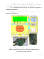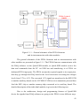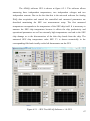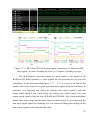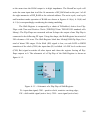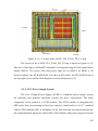
1
Graduating university: Ministry of Education and Science of the Russian Federation National Research Tomsk Polytechnic University Institute of Physics and Technology Department of Electronics and Automation of Nuclear Plants Guiding Institute: The Academy of Sciences of the Czech Republic Nuclear Physics Institute Nuclear Spectroscopy Department Digital acquisition software and hardware for SEU chip test By Vasily S. Mikhaylov A graduation work Submitted in fulfillment of the graduation work requirements for the qualification of physical engineer. Approved by: Project advisor (NPI): Dr. Vasilij Kushpil Technical consultant (TPU): Prof. S.N. Liventsov Linguistic advisor (TPU): Dr. N.G. Novikova Řež near Prague, Tomsk – 2013 Abstract Achieving the sustainability of electronics against the radiation is a very important task facing the ultra relativistic physics scientists. Single event upset effect is one of the common effects which occur during the irradiation of electronics, especially SRAMs as they consist of a huge amount of transistors sensitive to the upcoming energy particles. This problem is notably significant nowadays due to the fact that the dimensions and correspondingly supply voltages of the transistors become very small and the probability that energy of ionizing particle will be enough to cause the SEU effect highly increased. The SEU effect is a very of concern for the high energy physics detectors electronics including the ALICE detector electronics used for the ultra relativistic particle investigation with LHC in CERN. This graduation work addresses these issues related to the memory test during the charged particles irradiation. In particular, this graduation work describes simulations of SEU effect using the SPICE model of the RAM cell to predict probable level of the SEU rates. The main aim of the graduation work is to describe the hardware, the firmware and the software of digital acquisition system (DAQ) developed by Nuclear Physics Institute (NPI) Řež group used for the tests of SEU chip designed for investigation of the SEU rates and levels in electronics proposed to be used for the ALICE ITS upgrade. It is important to highlight that despite the fact that the DAQ system was developed for radiation test of SEU chip, the DAQ system is an absolutely independent complete system providing the possibility to investigate any other memory chip or other digital structure. This graduation work comprehensively describes the developed DAQ hardware and its interconnections allowing processing the high-level experiments with memories or other digital structures of modern integrated circuits. The main contribution of the graduation work author is the development of the firmware and software modules, such as “SEU Test FPGA Firmware v 1.0” module allowing fast 2 and robust FPGA operation giving the possibility to interact with SEU chip from DAQ software, the „SEU Test DAQ Software v 1.0“ providing the opportunity of both analog and digital data acquisition with the help of FPGA firmware, the “SEU Test ADAQ Software v 1.0” providing the opportunity of the analog data acquisition allowing measuring the important operating parameters of the DAQ system itself, and modernization of the additional software “MCL-2 precision positioning system module” allowing control of the MCL-2 positioning hardware module and “ALICE LVPS control v 2.0” software providing the control of the LVPS module supplying the power to the whole DAQ system. At the simulation part of the work the SPICE model of the 4T RAM cell was developed, proposed model of critical charge calculation based on additional resistor connection was discussed and expected value of critical charge resulting in the single event upset achieved for the investigated chip that is about 590pC (about 1.23*105MIP). Test measurement setup of the developed DAQ system and the test results are also described in the work. During the first measurement test we prepared the necessary background to the real SEU chip test irradiation and investigated that the beam profile has Gaussian shape quite appropriate for the SEU chip irradiation. Unfortunately, during the laboratory tests of the SEU ALICE_ITS_TJ180_TD_V1 chip we investigated it has some design issues and cannot be operated, that was confirmed by the Cagliary group when they tested their own DAQ system for the SEU chip. Here we came to the conclusion that on the one hand we need to wait for the properly designed chip to be able to acquire the data and perform next irradiation experiments with SEU chip. On the other hand we ensured that our developed DAQ system is working properly and because it is a multipurpose DAQ system we can perform the experiments with irradiation of any other memories or chips. 3 Acknowledgements I would like to express my profound gratitude to my chief Dr. Vasilij Kushpil for granting the job, giving me freedom to schedule my work time and teaching me so many things all along my work. I would also like to thank Dr. Vladimir Wagner for getting me into the Nuclear Physics Institute, resolving so many documental issues and providing much help while I was staying in foreign country. Also I want to thank Dr. Jozef Ferencei who helped me much with communication with other staff and students working in the department and for the help with solving financial and organizational issues for our project experiment. I would like to thank Josef Špalek who helped us with the measurement setup tuning and provided the LVDS board with 4m cable connection of the DAQ to SEU PCB board. I express the great gratitude to Dr. Michal Šumbera for employing me and granting the good financing source both for my personal needs and for required project equipment. I am very grateful to Dr. Svetlana Kushpil for the very nice welcome and provision of information about different facilities in Czech Republic. I am saying great thanks to the head of my department and my university supervisor Prof. Sergey N. Liventsov for additional financial support and making this internship research possible. Finally I am very thankful for everyone I worked and communicated with during this work at Nuclear Physics Institute of ASCR. Last but surely not least, I am indebted to my mother for endless care and support throughout my internship research. 4 Table of contents 1. Introduction ............................................................................................................... 6 2. SEU Effect Theory .................................................................................................. 14 2.1 Soft Error Overview .............................................................................................. 15 2.2 Soft Error Mechanism ........................................................................................... 17 2.3 Single Event Upsets in Integrated Circuits ........................................................... 20 3. SPICE RAM Cell Critical Charge Simulation ........................................................ 24 4. DAQ Hardware ....................................................................................................... 32 5. DAQ Firmware ........................................................................................................ 40 5.1. FPGA Firmware ................................................................................................ 40 5.2. MCU Firmware ................................................................................................. 48 6. DAQ Software ......................................................................................................... 55 6.1. Digital DAQ Software....................................................................................... 56 6.2. Analog DAQ Software ...................................................................................... 66 6.3. Additional Software .......................................................................................... 71 6.3.1. MCL-2 Positioning System Software ......................................................... 71 6.3.2. LVPS Control Software .............................................................................. 73 7. Measurement Setup and Memory Chip Tests ......................................................... 79 7.1. U-120M NPI Řež Cyclotron Facility ................................................................... 79 7.2. Test Measurement Setup and Beam Profile Scan at Cyclotron ........................... 81 7.3. Testing of the SEU Chip Operation ..................................................................... 88 8. Conclusion and future work .................................................................................... 93 Appendices .................................................................................................................. 97 A. Supplementary Hardware Description ................................................................... 97 A.1. ALICE_ITS_TJ180_TD_V1 Test Chip .......................................................... 97 A.2. LVP/S Power Supply System........................................................................ 102 A.3. MCL-2 Precision Positioning System ........................................................... 104 A.4. UNIDOS Dose/Rate Meter ........................................................................... 106 B. Full schematic of “SEU Test FPGA Firmware v 1.0” ......................................... 108 References ................................................................................................................. 109 5 1. Introduction This chapter describes the main reasons for soft error problem in modern chips and explains general causes why the number of soft error rate in chips grown during last decades. The chapter shortly discuss the effort of ALICE Nuclear Physics Institute (NPI) Řež group ALICE ITS upgrade and denotes the resulting reliability development of DAQ system for the tests of digital structures used in particle pixel detectors, thereby outlining the motivation behind this research. During the last thirty years the radiation influence on electronic circuits become very important task for scientific research. These studies are extremely vital due to the fact that nowadays electronics consist of very small structures such as transistors which are very susceptible even for little doses of radiation. As it is postulated by the Moore’s law the electronic chips technologies scaling decreased in quite a reasonable proportion from the end of the previous century till the beginning of current century. It especially affected the area of integrated circuits where the semiconductor technologies can be considered as a breakthrough in terms of device workability. The number of semiconductor transistors which make up the chips is doubled in each new technology generation that usually takes place in every three years. Of course, other chip operating parameters get better as well, in particular operating frequency enlarged by 44% and energy consumption used for transistor switching decreased by 65% [1Error! Reference source not found.]. Also the price per transistor on a chip has dropped dramatically since Intel was founded in 1968. Some people estimate that the price of a transistor is now about the same as that of one printed newspaper character. It looks really amazingly that nowadays average transistor gate length is about 32 nanometers while more than 60 million 32nm transistors could fit onto the head of a pin [2]. But all these advantages 6 and benefits of extremely small sized transistors usage has its down side expressed in different quality and reliability issues that can presently be very crucial. For example, sub-100 nanometer integrated circuits are very sensitive to various disturbances during the operation because of shortened sizes and decreased power supply voltage levels. These disturbances can be caused by such internal operational problems of the chip as supply voltage noise, ground-level noise, signal coupling and leakage currents, by variation in chip parameters during the production such as threshold voltage, channel length and channel width or by external sources such as ionizing radioactive high energy particles [3]. The point is that internal operational problems and production problems can be eliminated or at least reduced to some reasonable level by better grounding or advanced process control, today the most difficultly solved problem is still ionizing radiation. It is obvious that decrease of the transistors and correspondingly whole devise sizes leads to an enlarged influence of radiation effects, specifically single event radiation (SER), on the performance of science, military, space, and commercial electronics [4]. The study of radiation effects can be done in multiple ways such as analysis of total dose radiation, neutron-displacement damage, dose-rate radiation, and single event radiation. Each way assumes its own method of analysis, measurements of errors, and possibilities to elimination. While all four areas are strongly important to provide a comprehensive view of robustness of electronic devices during irradiation this work centers on the impact of single event upset (SEU) radiation. As it has already been postulated the operational problems can be caused by internal chips sources or by external sources. This statement presumes that not only the operational or process variation problems can happen as the internal chip issue but also alpha particles can be irradiated from the chip packaging material. As external sources two sources of radiation can be considered: high energy neutrons that appear with cosmic rays and any other particles coming from the human designed high energy radiation sources such as external irradiation of protons or 7 alpha particle during the ultra relativistic physics experiments [5]. However, the most noticeable effect is coming from transitions of high energy particles produced in accelerators, where the particle flux density is very high. As it was previously stated SEU research is a key reliability concern for reducing the influence of ionising radiation in digital structures used at accelerator facilities such as Large Hadron Collider (LHC) at CERN [6]. The ALICE (A Large Ion Collider Experiment) CERN Collaboration has built a dedicated heavy-ion detector to exploit the unique physics potential of nucleus-nucleus interactions at LHC energies [7]. The aim is to study the physics of strongly interacting matter at extreme energy densities, where the formation of a new phase of matter, the quarkgluon plasma, is expected. The existence of such a phase and its properties are key issues in Quantum chromodynamics for the understanding of confinement and of chiral-symmetry restoration. For this purpose, the comprehensive study of the hadrons, electrons, muons and photons produced in the collision of heavy nuclei are carried out. ALICE is also studying proton-proton collisions both as a comparison with lead-lead collisions and in physics areas where Alice is competitive with other LHC experiments. The upgrade strategy of ALICE collaboration, recently endorsed by LHC Committee, includes a new silicon tracker with greatly improved features in terms of: determination of the impact parameter (d0) to the primary vertex, tracking efficiency, and readout rate capabilities [8]. Such a new silicon tracker will allow ALICE to measure charm and beauty production in Pb-Pb collisions with sufficient statistical accuracy down to very low transverse momentum, measure charm baryons and perform exclusive measurements of beauty production. These measurements are essential in order to understand the energy loss mechanism and thermalization of heavy quarks in the Quark-Gluon Plasma state. The radiation levels expected for the High Luminosity (after the second long shutdown in 2018) phase impose stringent requirements on the radiation hardness of 8 the innermost layers of the ALICE Inner Tracker System (ITS). The yearly radiation levels expected for the innermost layer (radius=22 mm), including safety-factor of 4, are 700 krad and 1013 neq/cm2 for a collected data set corresponding to 10 nb -1 Pb-Pb and 6 nb-1 p-p collisions. About 1011 interactions should be recorded at the interaction rate of about 50 kHz [8]. The ALICE detector is modified to allow the readout of all interactions. It is crucial to ensure full functionality in terms of radiation hardness especially for the innermost layer. Figure 1.1 – Hybrid technology pixel detector during the irradiation Two general technological approaches for the new particle detectors are now considered for the ALICE ITS upgrade: new monolithic pixel technology where the CMOS chip readout system is internally combined with the detector layer itself and well known hybrid pixel technology where the readout chips are connected to detector part by metal bump bonds [9]. In both technological approaches the impact of the single upset events is a very crucial concern requiring the comprehensive 9 testing and analysis. The influence of the high energy particles can be easily illustrated using the well known hybrid technology pixel detector during the irradiation shown at figure 1.1. In this case the charged particle goes through the device starting from its sensor part and continuing in the metal bump and then in the readout electronics chip as shown by the particle track line. In the sensor part the particle goes through the depletion zone of doped silicon layer creating the cylindrical track of electron-hole pairs with a small radius less then a micrometer and a very dense concentration of charge carriers. Then due to potential difference between the bias voltage electrode and the insulator the created carriers travel to the diode implant where they are collected and transformed to regular electrical signal and go through the bump to the readout electronics chip. But if a particle after going through the sensor part still has a viable energy it can cause the single event upset described in chapter two inside the readout chip and cause the data damage. To simulate the impact of the expected radiation level influence on different memories used as readout for pixel detectors in the ALICE ITS systematic irradiation tests using protons were carried out throughout 2012 and onwards on various sensor, analog and digital test structures in order to: – study their performance, stability and annealing behavior before and after protons irradiation as the basis for a recommendation of a technology to be chosen as baseline for the development of future ITS prototype detectors; – gain experience in the operation of new ITS structures under realistic operational conditions; – provide further input for simulation studies on the expected detector performance under upgrade run conditions. To disentangle the various possible radiation-induced effects 3 types of structures are currently under investigation: basic structures (diodes and transistors), digital structures (RAM’s and Shift Registers) and full sensor structures (including analog and digital front end electronics). 10 The ALICE Nuclear Physics Institute (NPI) Řež group has been a recognized and respected member of the ALICE collaboration for 20 years already. Our group was involved in a number of different ALICE projects such as development, tests and analysis of the Silicon Drift Detectors and development low voltage power supply (LVPS) system [10]. The contribution of ALICE Nuclear Physics Institute (NPI) Řež group to this effort is development of the comprehensive and robust test system for testing of the digital structures. A chip for dedicated SEU tests has been designed and implemented in TowerJazz 0.18 µm CMOS technology (SEU TJ180) consisting of [11]: – SP_RAM Single Port RAM block containing an array of 16 single port RAM memories "1024@16 bits"; – DP_RAM Double port block containing an array of 8 dual port RAM memories "2048@16 bits"; – Shift Register block with a 16 bit 32K stages. Altogether, these structures have 81920 memory cells to test the stability and reliability of switching states during irradiation with charged particles (Figure 1.2). Figure 1.2 – Layout of the ALICE_ITS_TJ180_TD_V1 chip 11 The developed test system consists of a SEU device kit board, a FPGA board for connectivity via USB and a DAQ board for the acquisition of analog data. Test measurements using this system will be carried out using mono-energetic α-sources and proton beams from a cyclotron. Dedicated software with GUI allows a convenient operation and analysis of the test data. Objectives of the test measurements are to identify the distribution of SEU across the test structures and the evaluation of the SEU cross section as a function of proton energy. The mapping of SEU can also be measured using picosecond infrared lasers. As mentioned earlier, achieving the sustainability of electronics against the radiation is a very important task facing the ultra relativistic physics scientists. Single event upset effect is one of the common effects which occur during the irradiation of electronics, especially SRAMs as they consist of a huge amount of transistors sensitive to the upcoming energy particles. This problem is notably significant nowadays due to the fact that the dimensions and correspondingly supply voltages of the transistors become very small and the probability that energy of ionizing particle will be enough to cause the SEU effect highly increased. The SEU effect is a very of concern for the high energy physics detectors electronics including the ALICE detector electronics used for the ultra relativistic particle investigation with LHC in CERN. This graduation work addresses these issues related to a memory test during the charged particles irradiation. In particular, this work describes simulations of SEU effect using the SPICE model of the RAM cell to predict probable level of the SEU rates. The main aim of the graduation work is to describe the hardware, firmware and software of digital acquisition system (DAQ) used for the tests of SEU chip designed for investigation of the SEU rates and levels in electronics proposed to be used for the ALICE ITS upgrade. It is important to highlight that despite the fact that the DAQ system was developed for radiation test of SEU chip, the DAQ system is an absolutely independent complete system providing the possibility to investigate any other memory chip or other digital structure. 12 The graduation work is organized as follows. Chapter 2 provides an overview of SEU effect theory, the errors occurrence mechanism and main parameters affecting the errors occurrence. Chapter 3 proposes the basic SPICE model of RAM cell and characterizes the main parameters variations during the simulation of irradiation influence. Chapter 4 describes the DAQ hardware developed by Dr. Vasilij Kushpil for digital and analog data acquisition of irradiated digital structures. Chapter 5 reviews the DAQ firmware developed by Dr. Vasilij Kushpil and Vasily Mikhaylov for the correct and robust DAQ system operation. Chapter 6 describes the DAQ software developed by Vasily Mikhaylov and Dr. Svetlana Kushpil allowing the digital and analog data acquisition as well as simple online and offline data analysis. Chapter 7 proposes the laboratory test setup of DAQ system and the test measurement setup of this system at the NPI Řež cyclotron facility. Chapter 8 summarizes the contributions of this work and research and gives the conclusions. 13 2. SEU Effect Theory This chapter describes the main concerns considering the soft error effect in nanoscale chips, particularly in transistors which are used in RAMs. The chapter characterizes history and mechanism of soft errors occurrence, states the general causes why number of soft error rate in chips grew during the last decades, and identifies the main parameters substantial for SEU description. As it was described in the previous chapter the single upset event can occur when a high energy particle goes through the semiconductor electronic device. There the particle creates a dense track of electron-hole pairs along the particle track and thus produces a voltage transient at the corresponding node that collects the charge as shown at figure 2.1 [12]. This effect is also called a single event transient (SET). Reverse-biased p-n junction in transistor is the part that is most sensitive to such effects because of it is collecting charge very rapidly. It can happen that an amount of charge collected this way is enough to cause the SET which leads to a data damage in the form of flipping the logic state from high level state to low level state or other way round at the corresponding node. If such an effect occurs in one of transistors of the memory cell this event is called a single event upset (SEU). SEU effect itself does not lead to physical damage of the device and that is why it is also called “soft error”. Figure 2.1 – Simplistic view of alpha particle strike on a transistor and the resulting transient on the drain voltage [13] 14 Despite the fact that a “soft error” does not corrupt the chip physically, it still can cause an error for the proper chip operation and corresponding data loss. Due to the fact that energy enough for the “soft error” is much less then for the “hard error” when chip physically breaks the “soft error” rates (SER) can reach much higher limits comparing to the “hard error” rates. In a usual case hard error rates can reach 200 FIT (FIT means Failure In Time – one error per 4.54 days of chip operation) while the SER can reach up to 50.000 FIT per chip [14]. It is obvious that in radiation conditions this number increases in multiple times, so description and elimination of “soft errors” electronic chips produced with nanoscale technology is a very important point for the radiation tests and experiments. 2.1 Soft Error Overview The history of single event effects starts from the occurrence in electronics during ground nuclear experiments in 1954-1957 and space electronics tests during the 1960s [15], [16]. The first evidence of soft errors from α-particles in packaging materials was reported for dynamic random access memory in 1978 [17]. Nevertheless, the soft errors did not nave any really serious influence during aforementioned times because of the big dimensions and higher power supplying voltages of electronic elements used there and provided additional protection against single event upsets such as bigger capacitance of sensitive nodes and larger noise margin. But as it was already declared, during the time technology was scaling multiple times, while power supply voltage and capacitance of the nodes decreased by about 30% in every technology generation [18]. The decreasing of these parameters caused the decreasing in the signal charge responsible for a logic voltage level by factor two [19]. The charge which should have an ionized particle decreased because of this fact as well as because of the reduction of the chips dimensions that increased the probability of striking the node by the particle. Nevertheless the first 15 effect is more significant quantitatively and that is why the SER is increasing with technology scaling [20], [21]. Figure 2.1 – Soft error rate prediction for the semiconductors [22] Figure 2.1 shows the SER in semiconductor products as a function of technology process dimensions, where the data were collected by AMD, Intel, and Compaq. It is obvious from Figure 2.1 that semiconductor systems in sub-100nm technologies are very sensitive to soft errors. This results in the fact that modern microprocessor systems are developed with addition of soft error robust circuits [23], [24]. In fact, soft errors have always been a key reliability concern for missioncritical applications where a single error can lead to catastrophic failures in one case, and for severe environment applications where the heavy particle fluence lead to extremely high SER in another case. Example for the first case can be space-borne electronics or implantable medical equipment (e.g., cardiac defibrillators) while the prominent example of the second case applications is the reduction of the influence of ionising radiation in digital structures used at accelerator facilities such as Large Hadron Collider (LHC) at CERN. 16 2.2 Soft Error Mechanism The aforementioned SEU mechanism itself can consists of three general phases: (a) start of the event, (b) charge drift and (c) charge diffusion [14]. As shown at figure 2.2, in phase (a) the charged particle goes through the depletion zone of doped silicon layer creating the cylindrical track of electron-hole pairs with a small radius les then a micrometer and a very dense concentration of charge carriers. The particle’s linear energy transfer (LET) indicates the energy deposited per unit path length as a particle goes through the material and defines the amount of the charge created by the particle. Figure 2.2 – a-c) Charged particle hit causing loss of charge in reverse-biased p-n junction, d) the transient of current at corresponding node due to the particle hit [14] Generally, LET is defined by the energy deposition per unit length and calculated in MeV/cm and depends on the target material properties, but it can also be recalculated in the form where it becomes independent from the material properties, especially from its density with the help of dividing by the density ρ in mg/cm3 (for silicon ρ = 2.33 g/cm3) and presented in the MeV-cm2/mg [12]. It is possible to get the particle’s charge loss per unit path length from the particle’s LET, for example an LET of 97 MeV-cm2/mg is equal to a charge loss of 1 pC/μm in silicon. Accordingly, 17 the energy deposition value can be calculated from the known LET using the following formula in MeV [25]: Edep [MeV]=LET[MeV cm2 /mg] [mg/cm3 ] smax [cm] 2 2 2 In this formula s is a path length smax [cm]= 2L +c [cm] for device dimensions width and length a=b=L and c – device depth as shown at figure 2.3. Of course if particle hits material at an angle its past is upgraded corresponding to the cosine law divided by cosine of corresponding angle cos(Θ) and so forth. Figure 2.3 – Simplistic 3D view of the device hit by charged particle. In phase (b), electron-hole pairs generated during the particle penetration of silicon are quickly collected on the corresponding sides of the p-n junction because of the intensive electric field inside of depletion region [13]. Accordingly, holes travel to p-substrate that has the low potential while electrons travel to n-diffusion that has the high potential during the tens of picoseconds. Generated negative charged particles are increasing the depletion region during this phase as shown at figure 2.2(b) to the cone shape extending the charge collection volume where the size of the cone shape is inversely proportional to the substrate doping. In the last phase (c) the depletion region returns to the normal size and the residual charged carriers continue travelling to the corresponding nodes of p-n junction due to the regular diffusion mechanism. This process runs on until all the remained particles are collected or recombined with each other and can take up to few nanoseconds. 18 At figure 2.3(d) the transient of current at corresponding node due to the particle hit is represented. The amount of charge that is collected during the current transient and called collected charge Qcoll can be approximately calculated by the following formula [25]: Qcoll [C]= Edep [eV] q[C] WEHP [eV] In this formula q is the initial charge of the penetrating particle, for example for electron qe = 1.6022x10⁻¹⁹ C, and WEHP is the energy required for the electronhole pair creation, for example for Silicon WEHP = 3.6eV. Actually, the collected charge Qcoll cannot be calculated so simply and depends on multiple factors, such as device’s dimensions, structure of substrate and doping, variation of nodes biasing, type, energy and trajectory of the particle, the point where particle penetrated the device and the state of the device before the penetration. Of course, the Qcoll value is inversely dependent on the distance between the node and the point where the particle started the device penetration. Also, it should be taken into account that nodes in modern cells are placed quite near to each other, so when the particle hits one of the nodes it can also touch the another nearest one and result in formation of temporary bipolar transistor between nodes that will cause the increased probability of big charge collection. Correspondingly, the bigger the collected charge is for the investigated p-n junction, the bigger is the probability of soft error happening and if the charge is ever much bigger even the hard error damaging the device can occur. The fact that the cell collected some Qcoll charge lead to a single error upset event only if it outreaches a critical charge Qcrit, that is correspondingly defined as the minimum collected charge leading to the change of the cell state (“1” to “0” or vise versa) [12]. But if the collected charge is smaller than the critical charge calculated for this cell, the single event will not happen and the cell will remain its data properly. Accordingly, the critical charge can be considered as the main quantitative 19 parameter describing the ability to withstand the radiation flow for the certain investigated memory cell. For example, for the device with L x L dimensions, the critical charge causing the flip of the data state depends on the squared feature size (Qcrit ~ L2) and can be calculated by the following empirical formula [26]: Qcrit [C]=0.023[pC/ m2 ] L2 [ m2 ] Thus, using the aforementioned formulas we can get the formula that describes the possible value of the threshold LETthr for the irradiating particles that the investigated cell can withstand: LETthr [ Qcrit [C] WEHP [eV] eV ]= 2 mg cm q[C] [mg/cm3 ] smax [cm] For example, for the APEX FPGA the LETthr ≈ 100 keV/mg/cm2 while the LET during irradiation by the 30 MeV protons in Silicon = 15 keV/mg/cm 2 [27]. However, the critical charge and correspondingly LED are not constant during the different tests and for the different cells of the device because the way how the device reacts to the particle hit is described by the transient pulse form, and depends not only on the magnitude but on the temporal characteristics of the pulse as well [14], [19]. Accordingly, it is quite difficult to make the precise calculation or model of the critical charge Qcrit because it depends on the node capacitance and supplying voltage as well as on the restoration functions of corresponding nodes. 2.3 Single Event Upsets in Integrated Circuits Due to the fact, that different types of integrated circuits can be influenced by the irradiation we will shortly review how the simple logic circuits and various memories are influenced by the ionized particles causing the single event upsets. Memories can be both dynamic random access memory DRAM and static random 20 access memory SRAM. It is obvious, that logic circuits, DRAMs and SRAMs have different structure and that is why they should withstand irradiation differently. Charged particles can hit the combinational logic elements and can be latched by some of them. But usually the ionizing particle hit does not cause the single event upset because of three so called masking effects: logical masking, electrical masking, and latching window masking, which unavoidably exist in sequential logic circuits [19]. The elements of logic circuits (latches or register cells) are generally less influenced by the single events in comparison with SRAM, because the transistors used in these elements are much bigger then transistors used in SRAMs and correspondingly the capacitance and operating voltage is higher for them, that leads to the higher Qcrit required for the soft error occurrence. As it was stated, both DRAM and SRAM memories are more susceptible to soft errors, in comparison to logic circuits, because they have tighter packing density that mean smaller transistors and smaller required critical charge to cause the event, and also memories do not have masking mechanisms like for the logic circuits. It means that when a charged particle penetrate the cell or number of cells are situated nearby, it will change the state of the cells with relatively high probability and this corrupted data will remain until the moment when it is rewritten. Nowadays in DRAM signal charge is stored in 3D trench capacitors with the smaller junction volume and quite the same corresponding node capacitance comparing to the SRAM. Also it is important to note that the DRAM cells are quite frequently refreshed that works like a simple built-in error correction mechanism. This fact means that the system built on the DRAMs soft error rate is kept on almost the same level through the DRAM generations because the reduction of the SER is increased with approximately the same speed as memories packing density increases. The SRAM cell is constructed by two cross-coupled inverters and stores the written data as long as the power supplying voltage is on, so it does not need any 21 refreshing and does not have any built-in error-correction mechanism in comparison with the DRAM cell as shown at figure 2.4. Figure 2.4 – Two cross-coupled inverters comprising the simple memory cell The SRAM memory is named static RAM exactly because the inverters each consisting of one NMOS and one PMOS transistor are driving each other and keep the written data bit for all the operational time until they are rewritten. The SRAM memory cell represented at figure 2.5 consist of four transistors in the center used for the data storing and the two transistors on the left and on the right used to provide the access to the cell. Due to the fact that only two transistors from the four central ones are turned ON during the operation, corresponding to the stored value, the two transistors which are OFF are very sensitive to the particle hits and thus to single event upset, particularly at their p-n junction regions. Figure 2.5 –Six-transistor SRAM cell electronic schematic and layout. WL: word line, BL: bit line, BLB: complementary bit line. 22 Actually, SRAM nowadays can be easily integrated with logic circuits, it does not require any special refreshing mechanisms and has quite a rapid operating, that is why it becomes the mainly used element for the embedded memory construction, that fill the most of the die area in Systems on Chip (SoC) as it is shown at figure 2.6(a) [13]. Moreover, the area of the die used for the embedded memory placement continues increasing to provide the better performance as shown at figure 2.6(b). Figure 2.6 – a) Intel’s 65nm Xeon processor die; b) forecast for the memory area trend on SoC die (Semico Research Corp.). Summarizing the aforementioned information, we can say that nowadays SRAM single event upset sustainability is considered as the most important parameter for the whole System on Chip due to the fact that SRAM occupies the most of the die area and is the most sensitive element of SoC from the SEU sustainability point of view. Due to this fact the task of investigation of SRAM used for the particle detectors readout systems sustainability against the ionizing radiation in hard radiation conditions such as the ultra-relativistic particle physics experiments become very important today. 23 3. SPICE RAM Cell Critical Charge Simulation This chapter presents the brief review of SPICE simulation system, comprehensively describes the SPICE model of the 4T RAM cell and represents the results of simulation. The simulations of the critical charge is very important nowadays for all the memory chips used in radiation conditions. For example, the advent of circuit simulators, including PREDICT, ECAP, NET-1, CIRCUS, SPICE, and SCEPTRE, was directed, at least in part, by the need to model radiation effects in circuits [28], [29]. Micro-Cap 10 is an integrated schematic editor and mixed analog/digital simulator that provides an interactive sketch and simulate the environment for electronics engineers. Micro-Cap 10 blends a modern, intuitive interface with robust numerical algorithms to produce unparalleled levels of simulation power and ease of use. Familiar SPICE models are easy to be applied with the Micro-Cap 10 [30]. SPICE is a general-purpose circuit simulation program for nonlinear dc, nonlinear transient, and linear ac analysis. Circuits may contain resistors, capacitors, inductors, mutual inductors, independent voltage and current sources, four types of dependent sources, lossless and lossy transmission lines (two separate implementations), switches, uniform distributed RC lines, and the five most common semiconductor devices: diodes, BJTs, JFETs, MESFETs, and MOSFETs [31]. This system of the cell construction and simulation was chosen due to the fact that it allows easy and robust development and edition of the electronic circuits as well as descriptive and adjustable transient and dc analysis of the developed circuit. The first step of the 4T cell model development and simulations is to achieve the parameterized model of the single NMOS and PMOS transistors which should agree with the transistors used in the SEU chip. The Schichman-Hodges Model for the n-channel metal–oxide–semiconductor field-effect transistor (MOSFET) or 24 NMOS was used because it fully satisfies the requirements for the needed characteristics of transistors used in SEU chip. Using the NMOS with the chosen model the following schematic was developed to obtain the parameter-depended transistor characteristics shown at figure 3.1. In scheme the Gate terminal is connected to the voltage source Vgs to form the opening voltage for the transistor Q3. The Drain terminal is connected to the voltage source Vds to from the current going through the transistor from the Drain terminal to the Source terminal. Figure 3.1 – Schematic of the NMOS connected to two voltage sources The main parameterized function for NMOS model characterizing its properties is dependence of the drain-source current Ids on the drain-source voltage Vds with different constant gate-source voltages Vgs. In the Schichman-Hodges Model the function of Ids depends on multiple transistor parameters according to the following formula divided into three regions of Vds: I ds 0.0 ,Vgs Vth ; I ds KP Weff I ds KP Weff Leff Leff (1 Vds ) (Vgs Vth Vds ) Vds ,Vds Vgs Vth ; 2 (1 Vds ) (Vgs Vth )2 ,Vds Vgs Vth where KP [A/V2] is intrinsic transconductance parameter, Weff [µm] is effective gate width, Leff [µm] – is effective gate length, λ [V-1] – channel-length modulation, Vth – zero-bias threshold voltage. 25 Value of KP is calculated by the following formula: KP UO Cox , Cox ox Tox KP UO ox Tox where UO [cm2/(V∙s)] is surface carrier mobility, Cox [F/cm2] is oxide capacitance per unit gate area, εox [F/cm] – is oxide permittivity, Tox [cm] – gate oxide thickness. For both regions of Vds the values of parameters used for the Ids calculation were tuned to achieve the required form of Ids(Vds) function given by producer’s measurements [32]. The following values and parameter variation range were determined in the producer’s presentation: Weff = 0.22µm, Leff = 0.18µm, constant Vgs = 0.4V; 1.1V and variation of Vds in range from 0.0V to 2.1V [32]. The rest parameters were tuned in order to satisfy the producer’s requirements as follows: λ = 0.35 V-1, Vth = 0.36 V, UO = 90 cm2/(V∙s), εox (SiO2) = 3.9∙εox = 3.9∙8.854∙10-14 = 3.45∙10-13 F/cm, Tox = 3∙10-7 cm, KP = 1.03∙10-4 A/V2. Figure 3.2 – Comparison results of the simulated and measured Ids(Vds) dependences 26 The direct current (DC) analysis was performed for the developed scheme shown at figure 3.1 with implemented NMOS with parameterized model based on in the afore calculated parameters. The comparison results of the simulated and measured Ids(Vds) dependences are shown at figure 3.2. It is clear that the achieved simulated functional dependence of Ids on Vds quite adequately represents the Ids(Vds) dependence measured by the chip producers. The dependences for PMOS transistor are quite similar, so they are not presented here to avoid redundancy. The second step of the 4T cell model development and simulations is creation of model of the 4T RAM cell operated by two impulse voltage sources in Micro-Cap 10 software. 4T RAM cell is compiled by 2 NMOS transistors Q1 and Q4 and two PMOS transistors Q3 and Q5 connected as an inverter. All four transistors employ afore described parameterized MOSFET model.VDD voltage source is used as high level voltage source supplying the regular 1V. Impulse voltage source V2 is used as access elements which enables read and write access to cell and provides isolation when the cell is not accessed. Impulse voltage source V1 is used as a writing element which writes the data bit to the cell. The schematic of the developed 4T RAM cell is presented at figure 3.3. Figure 3.3 – Schematic of 4T RAM cell operated by two impulse voltage sources 27 The V1 impulse voltage source has 10MHz frequency, V2 impulse voltage source has 286kHz frequency, and they are combined in the way that the value stored in cell switches with frequency 286kHz. The time diagram of the cell switching operation achieved by transient analysis is shown at figure 3.4. This figure is the evidence that the developed 4T cell model is working correctly. Figure 3.4 – Time diagram of the cell switching operation achieved by transient analysis. V(4) – stored bit value, V(5) – inverted stored bit value, V(V1) – value of impulse voltage source V1, V(V2) – value of impulse voltage source V2 The final step of the 4T cell model development and simulations is to simulate afore described and developed 4T RAM cell model combined with the resistance used for the SEU critical charge estimation. The main idea is that if we connect an additional resistor between the drain and source nodes of one transistor, the total resistance of this triggering element will be changed as shown at figure 3.5. Using this model we can find the resistance value which forces the transistor to switch its state and therefore to switch the value stored in the cell. 28 Figure 3.5 – Parallel MOSFET and resistor connection changing the summary resistance In this case the critical charge can be calculated using the following equations: R L W x xON , 1 L Nd , e Nd e R W x L , W RON where μ – electron mobility for Si, ρ – resistivity of channel, Nd – donor concentration, R – resistance of channel, W, L, x – parameters of MOSFET. The developed model of RAM cell combined with the resistor to provide the critical value of channel resistance calculation is shown at figure 3.6. 29 Figure 3.6 – Model of RAM cell combined with the resistor to provide the critical value of channel resistance calculation In this model the “.NODESET V(B)=0” function is used to define the circuit initial conditions: voltage at point B V(B)=0V and voltage at point A V(A)=1V correspondingly, due to the fact that these voltages are related inversely. With help of Transient analysis simulation we found that at the resistance R=9.8Ohm the cell switches its state to V(B)=1V, V(A)=0V. It means that at R=9.8Ohm the charge in channel of transistor Q1 becomes critical. The investigated LVMOS transistor has the following parameters: µ=500 cm2/(V*s), Nd=9.298*1015cm-3, ROFF=150KOhm, RON=0.5Ohm, W=0.22µm, L=0.18µm. The value of critical charge calculated with the help of afore presented equations for 300µm Si is about 590pC that is equal to about 1.23*105MIP (minimum ionizing particles). This value is less than for the real process because a part of charge will recharge the output capacitance of MOSFET. We should expect the better result 30 from real measurement of the test structure. This method can be applied to investigate random switching of MOSFET under irradiation if MOSFET is biasing to the OFF state. Summarizing the aforementioned information, in this chapter we have overviewed the developed SPICE model of the 4T RAM cell, discussed the proposed model of critical charge calculation based on additional resistor connection and achieved the expected value of critical charge resulting in the single event upset event for the investigated chip that is about 590pC (about 1.23*105MIP). It is important to note that this value is less than for the real process because a part of charge will recharge the output capacitance of MOSFET. 31 4. DAQ Hardware This chapter presents the detailed description of hardware devices and modules used for the research. Methods and possibilities of hardware programming and controlling are discussed as well. Due to the complex measurement setup has been developed for the research purposes the distinctive features of individual devices should be considered to provide reliable and robust interconnection. Accordingly, in this chapter we discuss the main features and performance capabilities of the hardware used, design issues of the measurement setup integrally and operational conditions suitable for performing an experiment. Digital and Analog Data acquisition system (DAQ) is a system, developed for the acquisition the data and controlling of the SEU chip. The system can also be used for connection to addition devices such as MCL-2 precision positioning system via RS-232 interface (see appendix A.3 for more information). Figure 4.1 – Mechanical construction of DAQ The DAQ is composed of three individual parts as shown at figure 4.1: – Digital DAQ (DDAQ) board based on Quick-USB2 FPGA Developing Kit board (QUSB) to provide digital signals delivery to SEU chip with the help of USB interface; 32 – Analog DAQ and power supply board (ADAQ) for controlling power supply voltages and currents as well as temperature of the SEU chip; – SEU chip connecting board (SEUPCB) for chip package placement by standard bounding method. The DAQ system and interconnection scheme with reference to real modules photos is shown at figure 4.2. Figure 4.2 – Digital and Analog Data acquisition system scheme and its particular parts: Quick-USB2 FPGA Developing Kit board on the left and Analog DAQ board on the right. 33 The DDAQ is based on the QuickUSB Developing Kit that includes QuickUSB Cyclone II Evaluation Board and QuickUSB Module [33]. The QuickUSB module is used for the easy and reliable USB connection implementation for the DAQ system. The Cyclone II Evaluation Board has a QuickUSB module site and 0.1" headers that bring all the signals out. Altera EP2C20F256C7 Cyclone II FPGA on board contains over 1 Mbit of RAM available without reducing available logic and connects to nearly every pin of the QuickUSB module and extra I/O pins go to 0.1" headers [34]. Since the FPGA is an Altera Cyclone II, Quartus II Web Edition is used to design digital circuitry [35]. The FPGA is configured using QuickUSB libraries functions implemented inside the DAQ software described in chapter 6.1. The Starter Kit receives its power from the standard USB bus power supply as well as from power jack 5V/2A power supply on board. In addition, the I/O connectors for the QuickUSB module supply unregulated 5V and the I/O connectors for the FPGA supply regulated 3.3V. The Altera FPGA can get its clock from either the QuickUSB module (48MHz/30MHz), from a clock oscillator socket on board, and/or from a clock signal connected to the clock pin headers. All the digital I/O and control signals for SEU chip are formed at the FPGA board. The signals are going from the FPGA external pins to QUSB–ADAQ connector pins and then to ADAQ–SEUPCB connector pins. The Cyclone II FPGA contains four integrated PLLs and one of them is used to generate 10MHz clock for the SEU chip. The same PLL is also used to provide the communication of the DDAQ board and PC in so called Full Handshake mode to synchronize the SEU chip and USB interface for operation at 10MHz. Due to the fact that regular operation frequency of USB interface is 48MHz, we need to decrease this frequency to 10MHz that can be done by Full Handshake mode operation. In this mode each cycle of data transfer via USB connection is processed when the confirmation signal appears at the corresponding Quick-USB board READY pin. So, the synchronization in our case is done by sending the 10MHz signal shifted to the 50 degrees due to the timing 34 requirements to the READY pin (timing requirements are described at Quick-USB user guide [33]). The QUSB board also contains another popular serial interfaces such as I2C, SPI, RS-232 to provide external connections. In our case two RS-232 interface connectors provide auxiliary option to control the ADAQ board and/or MCL-2 precision positioning system. The control libraries are available for Windows, Linux and Mac PC operating systems [36]. ADAQ is a custom board developed in the NPI by Dr. Vasilij Kushpil to provide power supply to SEU chip, power supply parameters control such as voltages/currents and temperature control of the SEU chip itself. ADAQ consist of multiple electronic components to provide the described features. The seven TXB0108 8-Bit Bidirectional voltage-level translators with auto-direction sensing are used to convert 3.3V digital signals from FPGA to 1.8V digital signals feeding SEU chip I/O pins. The main processing element of the board providing the control of the above described parameters as well as connection via RS-232 interface with DAQ software on PC is Microcontroller Unit ATmega32 (MCU). ATmega32 is a high-performance, low-power AVR® 8-bit Microcontroller with various components and features such as advanced RISC architecture, nonvolatile program and data memories (32kB Flash, 1024B EEPROM, 2kB SRAM), JTAG and USART interfaces, internal calibrated RC oscillator, on-chip analog comparator, 32 programmable I/O lines, etc [37]. The MCU handle all the analog signals going from ADAQ analog elements and deliver them to DAQ software via RS-232 interface and vise versa. The power supply system is one of the most important parts of the ADAQ board. The setting of the SEU chip power supply can be implemented in two ways. The first and the best way is to use the digital-to-analog converter (DAC) paired with voltage regulators to precisely set the required voltage values from DAQ software. But there is a second “reserve” way to set the voltages values manually using 35 trimming resistors mounted on the board. One analog-to-digital converter (ADC) is used to provide measurement of voltages and currents of SEU chip power supply lines to ensure the proper and secure power supply. Moreover this power supply system allows estimating probable dependencies of SEU chip operation on varying the supply voltages values. Another ADC is used as safety feature paired with two resistance thermometers to ensure the secure operation of power supply of voltage stabilizers themselves concerning their temperatures. The aforementioned ADC paired with Pt-100 Platinum resistance temperature sensor with a temperature range of -200°C to 850°C is also used to control the SEU chip temperature [38]. During tests overheat can be crucial for the chip operation and PT-100 can be used to estimate probable dependences of single events accumulation on temperature. Normally 10MHz clock signal for SEU chip operation is provided by one of three external FPGA outputs connected to the chip clock input. But as an auxiliary feature ADAQ board comprises its own separate internal 10MHz oscillator to provide independent clock source for the chip. ADAQ board has two separated power supply lines of +5V and +3V for its own analog elements power supply and for SEU chip power supply correspondingly to avoid possible ground fault currents, leakage currents and other conditions that interfere the proper functioning of the system. The power is supplied to the ADAQ board from the LVPS module (for more information see appendix A.2). The SEUPCB is a simple small printed circuit board for connection of the chip to DAQ system without package placement by standard wire bounding method. The board is auxiliary PCB with 53x50mm dimensions and width of 1mm. The SEU chip board with all the placed elements and bonded SEU chip is shown at figure 2.2.3. The bonding of the SEU chip to SEUPCP board was done at the DESY Zeuthen bonding center with many help of Josef Ferencei [39]. The main feature of development of separate board for SEU chip placement is the possibility to place it to testing environment (proton beam) while the main DAQ system is situated in secure 36 place out of irradiation to ensure stable operation of its digital and analog elements. This is very crucial concern for cyclotron test because it is possible to maintain shielding versus proton beam but it is almost impossible to shield against neutron gas that exists all over the testing environment during the cyclotron operation (accumulated dose measured by dosimetry department staff is around 10mSv/h, see chapter 7.2 for more details). (a) (b) Figure 4.3 – Photo of the SEUPCB chip board with all the placed elements and bonded SEU chip: a) Bottom side view; b) Top side view. There are several options of implementation of data acquisition and control for SEU chip. The first option is the so called “slow test operation” when all the data to/from SEU chip is transferred through the developed DAQ system to the PC via USB interface. In this case all the data is processed within the DAQ software running on PC as well as the data comparison and estimation if single event happened or not. On the one hand this is the easiest option, on the other it limits the data exchange speed due to the USB speed exchange limitation. The second option is a so called “fast test operation” when general data exchange is proceeded between the SEU chip and FPGA. In this case the simple data processing algorithm is implemented inside 37 the FPGA. This algorithm allow the FPGA firmware to decide if single event occurred at any data cell and if so the information about corrupted data cell is transfer to the GUI running on the PC via USB interface. This option provides better data acquisition speed but requires more accurate testing and revision. The first option is already implemented to ensure the reliability of the system as a whole and the second option can be implemented to increase the data acquisition rate in future. (a) (b) Figure 4.4 – General flowchart of hardware operation in: a) data acquisition of single events accumulation; b) SEU chip operational status and power supply control. The embedded software and firmware is designed in the way to obtain two independent real time processes: first one to control SEU chip single events 38 accumulation and corresponding data exchange, second one to control the SEU chip operational status and power supply control. The flowchart of data acquisition of single events accumulation is shown at figure 2.2.4(a) and the flowchart of the SEU chip operational status and power supply control is shown at figure 2.2.4(b). The whole DAQ system setup connected with MCL-2 precision position stepping motors is shown at figure 2.2.5. Figure 4.5 – Digital and Analog Data acquisition system setup connected with MCL-2 precision position stepping motors Summarizing the aforementioned information, in this chapter we have presented an overview of all the main hardware developed for the SEU chip test measurement setup. All the other hardware used in the measurement setup is shortly reviewed in appendix A. We described the DAQ system providing and delivering digital signals and power supply for the SEU chip allowing reading and writing data in/out the chip in details. Thus, this chapter has provided the necessary background on hardware and its interconnections and states the necessity of usage of all the devices, paving the way for the following chapters. 39 5. DAQ Firmware This chapter provides the comprehensive description of developed DAQ firmware operation principles. The chapter discusses in details two independent firmware modules developed for this purposes, expounds the connection of firmware with DAQ software and reveals the hardware signal connections inside the DAQ board. Due to the fact that two independent channels for digital and analog data acquisition are used, two firmware modules were developed to operate these channels. The first firmware module „SEU Test FPGA Firmware v 1.0“ is designed to operate the digital data acquisition driving the FPGA module while the second firmware module “SEU Test MCU Firmware v 1.0” is designed to operate the analog data acquisition driving the microcontroller. The both modules are independent program components not relying on each other, but in complex allowing the trustworthy regular DAQ system operation. 5.1. FPGA Firmware The “SEU Test FPGA Firmware v 1.0” module was designed to be implemented with FPGA of QuickUSB board reviewed in chapter 4. The module was developed in the Altera Quartus II Web Edition software as a Block Diagram with multiple VHDL* block functions because this is the primary supported software by Altera company for all the Cyclone devices family. The reason for choosing the Block Diagram structure is the possibility of development of complex modifiable firmware that is perfectly suitable for SEU test and can be easily modified for other purposes. This firmware is one of the main contributions of this graduation work author to the SEU measurement setup which means that it was developed by Vasily Mikhaylov. *VHDL (very-high-speed integrated circuits hardware description language) is a hardware description language used in electronic design automation to describe digital and mixed-signal systems such as and integrated circuits [40]. 40 Figure 5.1.1 – General schematic of the FPGA firmware and its interconnection with other modules The general schematic of the FPGA firmware and its interconnection with other modules are presented at figure 5.1.1. The FPGA firmware communicates with the DAQ software via the Quick-USB module, so Quick-SUB module receive the data and commands from the PC via USB bus and transferring it to FPGA via dedicated FPGA input pins. The FPGA returns the required signals to its output pins, then they go through the DAQ board to the Level converters converting the voltages levels from 3.3V to 1.8V. The converted 1.8V signals are transferred to the SEU PCB or another auxiliary board via the LVCMOS LVDS receiver-transmitter pair and then feed the SEU chip or another memory/chip connected at its auxiliary board. The detailed description of the individual modules is given in the following text. Due to the architecture, design and programming features of QuickUSB device the signals from DAQ software are going to the FPGA in two different ways. 41 General data transfer signals such as clock, write enable, read enable, 9bit address and 16bit data signals have they own dedicated pins and simply pass to the FPGA internal pins from the QuickUSB board. Other signals important for the FPGA operation but not having dedicated pins are transported by special so called “command line” used for transferring user defined commands to FPGA. In fact, the commands are transferred to FPGA using the same general data line when cmd_data signal is HIGH. Accordingly, regular data transfer is processed when cmd_data signal is LOW. The usage of programming features allowing described data transfer with the help of DAQ software is presented in chapter 6.1. Figure 5.1.2 – The “Addrincr” function block schematic As it was described in chapter 4 SEU chip has 16bit data line, 15bit address line and control signals: CLK, SHIFT, BCAST, SEL and RESET required for proper operation. The 10MHz clock signal CLK for the SEU chip is generated in the FPGA’s PLL from the 48 MHz QuickUSB board clock and is directly feeding the SEU chip input. This PLL is also used to form another 10MHz clock phase shifted from first one to 51 degrees due to usage of Full Handshake QuickUSB operation mode requirements described in chapter 4.1. The schematic of “altpll” function block generated from ALT_PLL megafunction to operate the FPGA’s PLL is shown at figure 5.1.2. The 16bit data line of SEU chip is directly connected to external 16 bit bidirectional data line of FPGA using the parameterized tri-state buffer generated 42 from lpm_bustri Megafunction. But there is another situation regarding the address line of SEU chip due to the dimensions of address lines are different: the QuickUSB address line consists of 9bits and SEU address line consists of 15 bits, so they can not be directly connected to each other. This problem is solved by increasing 9 bit address line with the help of command data line in VHDL-module “Addrincr”. The 9 less significant bits are transferred by the general QuickUSB address line while rest 6 bits are transferred via command line then all the address bits are added together inside the “Addrincr” to form the required 15 bit address line (addrseu[14..0])feeding the SEU chip (memnum[3..0] + page[1..0] + addr9[8..0]). This function is currently used to form the 13 bits address (addr13[12..0]) for virtual RAM which consists of 10 less significant bits (page[1..0] + addr9[8..0]) to simulate address of one RAM block and 2 rest bits (sel[1..0]) to choose between virtual SP_RAM and DP_RAM. The schematic of “Addrincr” function block working on 10MHz clock from PLL to ensure the synchronous operation with virtual and SEU chip RAMs is shown at figure 5.1.3. Figure 5.1.3 – The “Addrincr” function block schematic Another important VHDL-function developed for the realization of connection between the DAQ software and FPGA firmware using general and command data transfer is the “Comminterpreter” function used for the interpretation of commands sent from DAQ software on PC to FPGA firmware. This function exploits standard “Case” structure to distinguish different commands using the general address bits as comparison parameter and the general data bits as the 43 transferred value. Each command has its unique 9 bit address defined in the “Comminterpreter” function as well as in DAQ software to avoid any command interpreting mistakes. This function is processed using the 48MHz USB clock for the command processing speed increasing and only when write enable (wen) and cmd_data signals are HIGH to ensure the fact of working with command line. In particular, such parameters as SHIFT (shiftseu), BCAST (bcastseu), SEL (selseu[1..0]) and RESET (resseu) assigned to the SEU chip input parameters as well as additional MEMSEU[3..0], PAGE[1..0] and DEVICE designed for internal FPGA usage are transferred via command line using “Comminterpreter” function. The SEU chip input parameters are described in appendix A.1 while MEMSEU and PAGE signals are used to form the RAM address and DEVICE command signal is used to switch between the virtual and the SEU chip RAM. The schematic of “Comminterpreter” function block is shown at figure 5.1.4. Figure 5.1.4 – The “Comminterpreter” function block schematic The developed firmware can operate in two principally different regimes – Internal RAM Simulator and External RAM Connection. The Internal RAM Simulator regime allows user to read/write data of the virtual RAM internally simulated in the FPGA module. This virtual internal RAM is absolutely identical in terms of addressing and data storage to the RAM of the SEU chip described in appendix A.1. General purpose of virtual RAM is to provide the opportunity of online test of measurement setup to ensure its operability in case of bad responses from 44 SEU chip as well as off-line test of measurement setup while the SEU chip is not connected. Virtual RAM can also be used in the following Firmware version upgrade as one of the parts providing the “fast test operation” described in chapter 4.2. The External RAM Connection regime is used when the SEU chip is connected allowing the direct manipulations with its memories. In this regime all the data goes from DAQ software on PC through the FPGA to the SEU chip input pins bypassing any internal FPGA usage or conversions. The switching between the virtual RAM and SEU chip RAM is done by multiplexing of the data flows from the RAMs to DAQ software by multiplexor connected to the DEVICE regime switching signal sent from the GUI. The multiplexing of the data flows going to the RAMs is done just by multiplying of DEVICE signal to the write enable signal of the corresponding memory (it is also important to mention that the cmd_data signal is multiplied to write enable and output enable signals going to both memories to ensure that they are not accessed during command transfer). Figure 5.1.5 – Schematics of the “LPM_RAM_IO” function block with I/O driven by “lpm_bustri0” function block The virtual RAM module of firmware is based on standard parameterized RAM with a single I/O port generated from Altera LPM_RAM_IO Megafunction with data bus width (LPM_WIDTH) parameter equal to 16 and address bus width (LPM_WIDTHAD) parameter equal to 13. The single I/O port is driven by 45 parameterized tri-state buffer generated from lpm_bustri Megafunction. Data-enable inputs of buffer are connected to the corresponding write enable and output enable signals from QuickUSB board as shown at figure 5.1.5. The LPM_RAM_IO RAM function block is used to simulate one memory block for SP_RAM and one memory block for DP_RAM in Internal RAM Simulator regime. This is realized by paging the virtual memory into two independent memory areas for SP_RAM and DP_RAM correspondingly. The two most significant bits of address input bus generated by “Addrincr” function block are used for the paging mechanism. Inclock input is fed by SEU chip 10MHz input clock, write enable (we) and output enable (outenab) input are fed by corresponding signals from the QuickUSB board and memory enable (memenab) input is fed by inverted cmd_data signal to ensure that RAM is not accessed during command transfer phases. Due to the fact that both internal and external 16 bit data bus pins are bidirectional the parameterized tri-state buffers generated from lpm_bustri megafunction are used to drive them. Data-enable inputs of both buffers are connected to the corresponding write enable and output enable signals from QuickUSB board in a similar way to the shown at figure 5.1.5. Following the requirements of the SEU chip operation write enable and output enable signal going to chip are inverted. All other control signals for the SEU chip are initially generated inside the “Comminterpreter” function block in the required form described in appendix A.1. Despite the fact that the operation of the FPGA internal virtual memory was already proven by the real data acquisition with help of DAQ system, the results of the simulation of its operation are done with help of standard Quartus 2 Simulator and presented at figure 5.1.6. There clock signal stands for 10MHz clock important for the memory block operation which form is defined in the simulation settings file, but the proper operation with 48MHz clock from USB bus was also proved in normal (not Full Handshake) Quick-USB operation mode. Address signal stands for the regular 10bits address bus which values are defined in the simulation settings file. 46 Datain signal stands for the input data feeding the internal memory which values are defined in the simulation settings file, while dataout signal stands for the output data from the internal memory which values are calculated during the simulation. Ren signal stands for read (output) enable signal, allowing the memory to be read out, wen signal stands for write enable signal, allowing the memory to be written in – both signals are defined in the simulation settings file. (a) (b) Figure 5.1.6 – Simulation results for internal FPGA memory: (a) – writing process; (b) – reading process. One can see from the afore presented figures, the data written to the memory during the reading process is successfully reproduced at the memory output during the reading process with exactly the same values that means that designed internal FPGA virtual memory is working properly. Summarizing the aforementioned information, in this chapter we discussed the „SEU Test FPGA Firmware v 1.0“ which downloaded to the FPGA module gives the possibility to interact with SEU chip from DAQ software. Two data transfer modes are used for it: the general data transfer allowing transferring the data to/from the memory and the command data transfer allowing transferring control commands intended for internal FPGA usage or for SEU chip operation. The two regimes of 47 firmware operation are implemented: the Internal RAM Simulator allowing testing the measurement setup while SEU chip is not presented using internal FPGA RAM and External RAM Connection allowing data exchange with SEU chip itself. The full schematic of developed firmware is presented in appendix B. Hereby the developed firmware allows operating the Digital DAQ FPGA module independently of SEU chip presence and provides the full range of features to communicate with SEU chip during the experiments. 5.2 MCU Firmware The “SEU Test Atmega32 Firmware v 0.06” (ADAQ firmware) module was designed to be implemented with microcontroller unit (MCU) Atmega32 of DAQ board described in chapter 4.2. The module was developed in the BasCom software as compiled code designed in Basic programming language. The reason for choosing the BasCom compiler is that it provides the possibility of easy and robust development of the firmware for microcontrollers based on basic. This firmware is very important for the SEU measurement setup and it was developed by Dr. Vasilij Kushpil. The developed firmware is designed to provide the possibility of analog data acquisition using ADAQ module. It fully promotes already declared feature of total separation of digital and analog data acquisition processes. ADAQ firmware provides easy and robust access to all the electronic modules of MCU itself and modules which are directly connected to and controlled by MCU. To provide the fast access to ADAQ module the communication via RS-232 interface is done at a 9600 baud rate. Due to the fact that MCU is connected with PC via RS-232 interface, all the used controlling commands are written in a simplified way, so the user can easily use any simple terminal software to achieve access to MCU module. For regular ADAQ operation and visual control of important parameters it is possible to use the general 48 DAQ or specialized ADAQ software described in chapter 6.1 and 6.2 correspondingly. Detailed schematic of ADAQ firmware is presented at figure 5.2.1. (-55 +125±0.5)oC (-55 +125±0.5)oC DS18B20 DT1 DS18B20 DT2 !tread:2 !tread:1 1.2 5.0V±0.013 0 1.0A±0.015 VA CH0 IA CH1 VB CH2 IB CH3 MCP3204 CS ADC1 12bit ATMEGA32 QFP44 WIRE CS0 … CS5 MCU CH0 … CH4 ADC0 … ADC4 5 !rdadc:0..4 DS1302 SPI RTC !vread:a/b !iread:a/b !mread:0..20000 CS !gdata:param !sdata:param 3 1.2 5.0V±1bit (-200 +500±0.3)oC MAX5400 CS VA MCP3550 DPOT1 8bit CS ADC2 22bit Pt100 to !vactrl:0/1 !vaset: 0..255 !tread:0 1.2 5.0V±1bit MAX5400 CS VB DPOT2 8bit !vbctrl:0/1 !vbset: 0..255 CS MCP4822 CH0 DAC3 10bit CH1 VX VY !sdac:x/y 0..1024 Figure 5.2.1 – Schematics of the ADAQ functional modules connection with MCU, corresponding commands and parameters limitations Each module controlled by the MCU has its own purpose and operating command defined in the ADAQ firmware. Every command starts with “!” symbol that indicates that MCU should consider the transferred data as a command. All the 49 commands have simple and intuitive spelling to provide easy usage. To provide the easier operation with developed firmware the “!help:” command prints all the used commands with the short description. The “!vers:” command or simple pressing the spacebar key shows the current firmware version. The “!msave:” and “!mload:” commands allow to save the other commands parameters such as desired voltages values to EEPROM memory inside the MCU and load them from it after the next connection procedure. The result of processing the “!help:” command is represented at figure 5.2.2. Figure 5.2.2 – The result of processing of “!help” command using the terminal “PUTTY” for the connection The 12bit analog digital converter ADC1 module (MCP3204 chip) provides the possibility to measure general power supply parameters, such as voltage in channel A (VA), voltage in channel B (VB), current in channel A (IA) and current in channel B (IB). These values can be measured with the help of three different 50 commands: “!vread:x”, “!iread:x” and “!mread:x”. The “!vread:x” command allows to process single measurement of the voltage level in millivolts at the channel A or at channel B and in each case “x” symbol should be replaced by “a” or “b” symbol correspondingly. These voltage levels can be measured in ranges from 1.2 to 5.0V with maximal statistical error of 0.013V. The voltage range is defined by the voltage setting range of digital potentiometers DPOT1 and DPOT2 while statistical error is defined by regular voltage measuring noise. The “!iread:x” command allows to process single measurement of the current at the channel A or at channel B in milliamperes and in each case “x” symbol should be replaced by “a” or “b” symbol correspondingly. These currents can be measured in ranges from 0 to 1.0A with maximal statistical error of 0.015V. The current measuring range is defined by the possible range of power supply currents while statistical error is defined by regular current noise. The “!mread:x” command allows to process the series of measurement of the aforementioned parameters VA, VB, IA and IB in the same time. The “x” symbol can be replaced by regular integer value that defines the number of measurements in range from 0 to 20000. The 0 value of “x” corresponds to infinite cycle of measurements which can be stopped by pressing of ESC keyboard button in terminal mode. Values from 1 to 10000 correspond to regular measurements number, where the 10000 limit is internally defined in the ADAQ firmware and can be enlarged if needed. Also, to define the numbers of measurements in this mode the command “!cycle:x” can be used, where “x” is the number of measurements corresponding to the afore described rules. The “!tdely:x” command allows to set the time delay between the ongoing measurements, where x is the time delay value in milliseconds in range from 10ms to 10000ms, that is initially equal to 10ms. Two same aforementioned 8bit digital potentiometers DPOT1 and DPOT2 (MAX5400 chips) are used for setting up the power supply voltage in range from 1.2 to 5.0V due to their technical limitations. The real accuracy of these setting can be 51 measured only by measuring the voltages by ADC1 module, so the accuracy is standardly defined in terms of possible 1bit error. The commands “!vactrl:x” and “!vbctrl:x” are used to turn on/off potentiometers outputs independently, where “x” should be replaced with “1” for turning on and “0” for turning off. The “!power:x” command can be used for the same purpose, but controlling both potentiometers at the same time. The commands “!vaset:x” and “!vbset:x” are used for setting the potentiometers voltage levels independently, where “x” should be replaced by the desired voltage level value to be set. The “!vabset:x” command can be used for the same purpose, but controlling both potentiometers at the same time. The voltage level value can be chosen binary form in range from 0 to 256, where 0 corresponds to 0V voltage level and 256 corresponds to 5.0V voltage level. The example of operational commands “!vactrl:1”, “!vbctrl:1”, “!mread:0” and the ADAQ firmware answers are shown at figure 5.2.3. Figure 5.2.3 – The example of voltages setting and parameters measurement cycle The 10bit digital analog converter DAC3 (MCP4822 chip) is an auxiliary module proving the possibility to send some analog data by two channels CH0 and CH1, i.e. set some voltages levels VX and VY. To set the corresponding voltage output value the “!sdac:d f” is used, where “d” symbol should be replaced by corresponding channel name “x” or “y” and “f” symbol should be replaced by regular integer value in the range from 0 to 1024. Due to the fact that this module is not currently in use there is no available information about statistical error. 52 The 22bit analog digital converter ADC2 (MCP3550 chip) is used to provide the temperature control for the memory chip investigated during the irradiation. It is connected to Pt100 temperature sensor that is self-sufficient module providing the measured data in analog form. The module has possible measured temperature range from -200 to +500 degrees Celsius and average statistical error of 0.3 degrees Celsius. The “!tread:0” command provides the possibility to achieve the measured data with the help of MCU. Two digital temperature sensors DT1 and DT2 (DS18B20) modules allow measuring the power supply stabilizers temperatures to avoid overheating. The temperatures can be measured by “!tread:x” command, where “x” correspond to the module number corresponding to number of power stabilizer – “1” or “2”. These temperatures can be measured in range from -55 to +125 degrees Celsius with average statistical error up to 0.5 degrees Celsius according to their specifications. The real time clock RTC module (DS1302 chip) is implemented to the ADAQ system to provide the possibility of its independent online time monitoring and synchronization. The module information about current date and time can be accessed by “!gdata:x”, where “x” corresponds to the requested value in the following terms: s – seconds, m – minutes, h – hours, d – days, n – months, y – years. The “!sdata:x” command allows to set the date and time to the desired value in the similar terms as the previous command. In addition to all the described external modules connected to and controlled by MCU, MCU itself has five analog digital converters ADC0…ADC4 which can be used for any further measurement purposes. The command “rdadc:x” allows to read information from the specified ADC, where “x” is the ADC number in range from 0 to 4. Summarizing the aforementioned information, this chapter discusses the “SEU Test Atmega32 Firmware v 0.06” (ADAQ firmware) module designed to be implemented with MCU Atmega32 of DAQ board. The firmware is designed to 53 provide the possibility of analog data acquisition using ADAQ module. It fully promotes already declared feature of total separation of digital and analog data acquisition processes. ADAQ firmware provides easy and robust access to all the electronic modules of MCU itself and modules which are directly connected to and controlled by MCU. 54 6. DAQ Software This chapter gives the exhaustive description of developed DAQ software in terms of programming, modification and operation principles. The chapter discusses in details the features of developed software, ways of analog and digital data acquisition processes distinguishing and interaction with DAQ firmware. The additional developed software providing important extra features to the system are described as well. As it was already described in chapters 4 and 5 the DAQ system is divided into two independent subsystems for digital and analog data acquisition. The two different ways of such division are implemented in terms of software. The first way is to use the DAQ primary software module allowing acquiring both digital and analog data in two independent processes. The second way is to use the DAQ primary software module for digital data acquisition and the DAQ secondary software module for analog data acquisition and control. Both ways have they own pros and cons: while exploitation of the one primary software for both processes allows easier program control, the exploitation of two independent software modules allows more detailed analog data acquisition due to the widening of the data graphs and total independence of two DAQ software systems. Due to two extra software modules were modernized and implemented for the SEU Test Measurement Setup System they are shortly described in this chapter. Accordingly the modernized LVPS software module control allowing the DAQ system power supply via TCP/IP and RS-232 protocols and the modernized MCL-2 driver system control software module allowing movement of SEU chip setup across X and Y axes within the proton beam. 55 6.1. Digital DAQ Software The „SEU Test DAQ Software v 1.0“ is a general software tool providing the opportunity of the both analog and digital data acquisition but mainly concerned the digital data form DAQ. This software is one of the main contributions of this graduation work author to the SEU measurement setup and actually it was developed by Vasily Mikhaylov and Dr. Svetlana Kushpil. Figure 6.1.1 – SEU Test DAQ Software v 1.0 The software allows measuring the digital data from the memories connected to DAQ hardware: virtual memories simulated inside the QuickUSB FPGA board chip, real SEU chip memories or any other compatible memories connected to the DAQ hardware trough the external connectors. This system provides not only the possibility of data acquisition but also the possibility of simple data analysis. This analysis function can be accessed in both on-line and off-line operation modes and can be used to analyze received data during the test or to analyze already collected data in off-line mode when no DAQ hardware is presented. The system provides the 56 possibility to communicate with memory via DAQ hardware, mainly via FPGA module and an extra feature to configure the module using the same USB connection. The detailed software description is presented in the following text, while the “SEU Test DAQ Software v 1.0” graphical user interface (GUI) during the operation is shown at figure 6.1.1. All the general and command data is read and/or written via QuickUSB module using the USB interface. According to that the special functions of the QuickUSB library are used for these purposes such as QuickUsbWriteData, QuickUsbReadData, QuickUsbWriteCommand QuickUsbWritePort, QuickUsbStartFpgaConfiguration etc. These library functions are described further in chapter when they are used in program. As it was explained before in chapter 5.1 lengths of address buses of QuickUSB module and SEU chip are different. The minor 9 address bits are transferred directly from QuickUSB address bus to SEU chip address bus while the rest 6 major address bits are transferred to FPGA via command data line using the QuickUSB library function QuickUsbWriteCommand as described in chapter 5.1. These major data bits correspond to 4 bits for selection of the memory block (1 of 16 for SP_RAM or 1 of 8 for DP_RAM) and 2 address bits that we will call “paging” bits. For example, to read the 2048 bytes of one SP_RAM memory block the following 2-step procedure is done: two “paging” bits “00” are transferred via command line initiating first “page”, then the first 1024 data bytes are transferred using QuickUsbReadData library function, then the second memory “page” is chosen by command line setting “01” paging bits and second 1024 data bytes are transferred. The similar procedure is done for DP_RAM but in 4 steps. Due to the data read or written from/to the memories via QuickUSB module is presented as simple byte sequence, for each transported data block it should be converted to the array that can be easily represented in the digital graph. The transferred data encounters 1024 words ∙ 16 bit = 2048 bytes for one SP_RAM 57 memory block, 2048 words ∙ 16 bit = 4096 bytes for one DP_RAM memory block and 16 bit 32K stages = 4096 bytes for Shift Register correspondingly. So, the data sequences should be converted to 1024×16 bit array (16384 data points) for one SP_RAM block, 2048×16 bit arrays (32768 data points) for one DP_RAM block and 2048×16 bit arrays (32768 data points) for the whole Shift Register correspondingly. This conversion is done internally after data read/write procedure and the resulting 2D data points array is saved in the PC memory, until it is rewritten by the next data flow. The resulting 2D array of memory points is represented in the graph in the GUI with the help of PlotIntensity LabWindows function. Every data point is shown in the graph as a small colored line at the corresponding X-Y position where X has 16 bits length and Y has length of 1024 for SP_RAM or 2048 for DP_RAM. The color is defined in a color array corresponding to possible data point values. Regularly we are reading/writing simple bits, so white color corresponds to “0”bit and red color corresponds to “1”bit, but if we are accumulating bits in corresponding array points, other colors are used for the values representation. The scale for color representation is the number of possible data point values corresponding to different colors, it is initially set for 13 values from 0 to 12, but scale can be changed using the status bar commands in the range from 2 to 128 (for more information on using status bar see the following information is this chapter). The transferred data is shown in the right part of the GUI divided into three graphs shown at right at figure 6.1.1: the left top graph corresponds to the SP_RAM data, the right top graph corresponds to the DP_RAM data and the bottom graph corresponds to the Shift Register data. To choose which memory types should be read and/or written three radio buttons are implemented in the GUI named correspondingly “SP_RAM”, “DP_RAM” and “SH_REG” for each memory types. To provide simple online data analysis functions the developed software has the possibility of data transfer operation in five different modes: Standard NoError 58 mode, ErrorSUB mode, ErrorADD mode, DataSUB mode and DataADD mode. Every mode can be processed in cyclic regime allowing continuous data transfer and is initialized by the “CYC” radiobutton. Each cycle processed in few tenths of seconds during “slow test operation” described in chapter 4.2. The first Standard NoError operational mode provides the possibility of regular read or write cycle by pressing “Read Test” or “Write Test” buttons and the data transferred during the cycle is represented on the graph as it is. The second ErrorSUB mode gives the possibility of simple data comparison process and it is the main mode for online SEU evaluation. At first some data is written to the SEU chip memories and is saved in PC in the special memory array, then the reading procedure takes place and the read data is compared to the written data. The difference in data arrays is shown on the graph, for example if all the written data is the same as the read data, all the graph will be colored white, but if SEU error occurred in some cell of the SEU chip memory, the bit corresponding to this cell will be colored red. This mode can be run in cyclic regime, so after each new data read cycle the read data will be compared to the first-written data and the difference will be shown in the graph. The third ErrorADD mode allows accumulation of error bits in PC in special memory array and after each new data read cycle the accumulated error data is shown in the graph. Accordingly, to correctly process these two modes the user should at first process data-write cycle and then process any number of reading cycles to compare the read and written data and analyze SEU accumulation over the time. The fourth DataSUB mode is intended for simple online data subtraction, so when it is processed the data read from SEU chip is saved inside the PC memory and is shown in the graph. In the next cycle the new read data is subtracted from the previous one point by point and the result is saved inside the PC memory and shown on the graph and so on. The fifth DataADD mode is similar to DataSUB mode, but in contrast to it the new read data is added to the previous one and the result is saved inside the PC memory and is shown in the graph. These two modes are developed for 59 further usage, for example they can be useful coupled with some data counter or if the SEU accumulation will be investigated starting with the all-zero SEU chip memory setup. The online analysis includes not only the representation of SEU events on the graph, but also the calculation of general quantitative values explaining the impact of occurred SEU events. Processing the ErrorSUB or ErrorADD modes the calculation of SEU events total number is done individually for each of the memories and then summarized to represent the total number of events in the whole SEU chip. These values are shown near the data and error representation graphs in fields named “SP_RAM SEU N”, “DP_RAM SEU N”, “SHIFT REG SEU N” for each memory type correspondingly and the field named “TOTAL SEU N” in the right bottom corner of GUI represents the total number of events for the whole SEU chip. In addition to it the Cross-sections for all the calculated events numbers are calculated based on the following formula: Cross-section [cm2 ]= Total SEU events number Radiation intensity [1/(cm2 sec)] In the aforementioned formula Radiation intensity is set in the Setting window of the GUI by the user for each individual experiment. The Settings window can be called by the “Settings” button in the left bottom part of the main GUI window. In this window the user can also set numbers of COM-ports for MCL-2 positioning system and Analog DAQ connection. Two supplementary testing functions can be called from the setting window by buttons “Make Chess 2048” and “Make Chess 4096”. Both these functions provide the possibility to create the initial file for writing to the SEU chip memories consisting of zeros and ones in the so-called chessboard layout order with special mixing to ensure correct operation as shown at \figure 6.1.2 for the DP_RAM. These functions are primarily used for system operation tests and do not take part in real experiments or measurements. 60 Actually there are several ways of achieving the initial files with data to be written to the SEU chip memories. This data files can be created by the aforementioned “Make Chess 2048” and “Make Chess 4096” functions, old data files that were read can be used or data file with necessary content can be created manually in any data file editor such as Windows Notepad [41] or WinHex [42]. The write-process can be performed in two ways: automatic or manual by changing the state of the “Auto” checkbox in the left bottom of GUI. In the manual mode when user presses the “Write test” button files to write to all the selected memories should be chosen manually one by one. In automatic mode software processes writing procedure from the files that should exist in the same directory as the software and named “sp_ram_init_bin.data”, “dp_ram_init_bin.data” and “sh_reg_init_bin.data” correspondingly for each memory. Figure 6.1.2 – Initial data in chessboard layout order with special mixing to ensure correct operation When any test procedure is running the one of the LEDs “Run Read” or “Run Write” situated above the test buttons is lighted up, in other case LED “Active” is lighted up and indicates that system is ready for measurement. To stop the procedure 61 that is run in cyclic mode the user can press the “Stop” button situated near the test button or uncheck the “CYC” radio button. In the left top corner of GUI three buttons and corresponding LEDs are situated to control the hardware connection as well as some supplementary information. First from the left button and LED are presented as the single LED “Quick-USB” and are used to control the connection of the QuickUSB board. Field next to the right indicates the name of QuickUSB device if it is connected. Next field shows the date and time from the Analog DAQ that is mainly used for logging. Next button first from the top is used to control the connection of the MCL-2 positioning board and LED near it indicates if it is connected. The lower button nearby is used to control the connection of the Analog DAQ board and LED near it indicates if it is connected as well. After the software launch connection of the Quick-USB module and Analog DAQ module is inspected, the appropriate messages pop up and are stated in the status bar. Then software date and time are synchronized to the time of PC and directory “data” is created to provide the possibility of data storing. After that the previous settings are loaded from the “settings.txt” file and single measurement of Analog DAQ values is processed. After all these steps the initialization procedure is completed and user can use the software for the essential purposes. Even if no hardware is connected, the user can load any already existed data file to be represented in the graph offline and simple analysis procedures can be done for this data as well as online. All the collected data can be saved to files of binary, hexadecimal and/or MAP format. Data can be saved to files of all the formats simultaneously or just to some file of chosen formats that are implemented by radio buttons named correspondingly “BF”, “HF” and “MF”. The data is saved to the automatically created special subdirectory with the name corresponding to the data and time of experiment like “Mon Sep 17 12.48.03 2012” inside “data” directory (“data” 62 directory should exist in same directory where the software executable file is situated). The binary data is saved as the file named “data_bin_X_Y.data” where X corresponds to the memory type: 0 for SP_RAM, 1 for DP_RAM and 2 for Shift Register while Y corresponds to the number of saved file on the account. Naming for the hexadecimal or MAP format files is quite the same but files would consist of “hex” or “map” pieces instead of the “bin” piece. The difference between formats is mainly the data representation and the required disk space. For example, the MAP-array data shown at figure 6.1.3 corresponds to binary sequence “33333333333333333333333333” or to hexsequence ”33 33 33 33 33 33 33 33 33 33 33 33 33”. To take in account the data capacity, the 2048 bytes of data that correspond to one memory block of SP_RAM requires exactly 2Kb of disk space to be stored in binary format, about 12Kb of disk space to be stored in hexadecimal format and about 50Kb of disk space to be stored in MAP format. Each data format has its own pros and cons: the data stored in the MAP format can be easily opened and analyzed even in simple notepad, but binary format provides much better data compression, so the choice of format is up to the user. Figure 6.1.3 – Example of MAP-data saved to the file Choosing the memory type (internal virtual FPGA memory or external memory, i.e. SEU chip) and memory block inside SP_RAM or DP_RAM is represented in the bottom left part GUI at figure 6.1.1. For these functions special command is sent via command line to the FPGA firmware to the reserved address 63 with the help of QuickUsbWriteCommand library function. The special command “Reset” used to control the state of Shift is situated nearby and is being sent using similar mechanism. The broadcast mode of the SEU chip operation is also controlled by the binary switch “Broadcast” situated nearby and indicating if this mode is ON, i.e. all the RAMs are accessed at the time with the same data. The mechanism of FPGA configuration with the firmware described in chapter 5.1 is implemented in the software to provide fast and easy possibility to change the whole FPGA operation model. The “ConfigureFPGA” button is used for this purpose running the procedure of configuration. At the first step the user chooses the firmware configuration file in “*.rbf” format, then QuickUsbStartFpgaConfiguration library function is processed to initiate the start of configuration. The second step is writing of values required for configuration to the QuickUSB FPGA ports and port directions by library commands QuickUsbWritePort and QuickUsbWritePortDir correspondingly. The configuration procedure itself is done in five steps by dividing the firmware file binary data into five parts and downloading these parts to the FPGA by QuickUsbWriteFpgaData library command. The ring slide on the GUI indicates how many of these five steps have already been done. When all the firmware configuration data is downloaded to the FPGA the library function QuickUsbIsFpgaConfigured is processed to ensure that the FPGA has been successfully configured. If the FPGA has been configured, the small LED lights up in yellow color and the confirmation message appears in the status bar. In other case the message tells that FPGA is not configured and the user can try to configure the FPGA again or to ensure that the firmware was developed correctly. The button “FPGA” situated in the right bottom part of the GUI is used to launch QuickUsbDiagCs.exe application. This application provides a reserve mechanism for FPGA configuration as well as for fine-tuning of the QuickUSB board ports and other features. To the right of the “FPGA” button software date and time synchronized to the PC are shown. To the left of the “FPGA” button the status bar is situated where almost every action that takes place during the software run is shown. 64 The status bar can also be used for the setting of additional parameters such as color scale for the aforementioned data point representation in the graph. To set the scale the user should type the “$scale XXX” command in the status bar where XXX is the new scale number in the range from 2 to 128. If the command is triggered and the scale is successfully set the appropriate message will appear in the status bar. All the commands start with “$” symbol and it is possible to use already typed commands again using the keyboard UP and DOWN arrows. To provide the possibility of measurements counting and additional data saving the log-files consisting of supplementary data from online analysis and analog DAQ are created in addition to files consisting of the memory data from SEU chip. Logging mechanism has its own checkbox “Log” that indicates if log-files should be created and saved or not. Two different log files are saved in the same directory where the data files are saved named “seu_analog.txt” and “SEU_ log.txt”. File “SEU_ log.txt” consists of the following information: Date and time of measurement, number of the measurement (fileindex), 3 temperature values from analog DAQ, 2 voltages and two currents from analog DAQ and total number of SEU events in all the investigated memories in the following format: “Wed Aug 15 15:05:45 2012 fileindex= 1 T1=50.7 T2=69.6 T3=63.6 VDD=2.824 VCC=4.773 IDD=1.74147 ICC=0.97203 TOTAL SEU: 511”. The file “seu_analog.txt” consists of the same data excluding the number of events and it is created only if analog DAQ is connected to this software. Every measured value has its own radio button “WF” near the value at the GUI that indicates if it should be saved in the files or not. For easier usage all the main features of the software described here are described as well in the help file that can be called by pressing “?” button in the very right top corner of the GUI, near to it the “X” button intended for exit from the software is situated. 65 The possibility of analog data acquisition that can be also provided by the general “SEU Test DAQ Software v 1.0” is quite similar to the operational functions of “SEU Test ADAQ Software v1.0” described in chapter 6.2. The „SEU Test DAQ Software v 1.0“ also provides the possibility to drive the MCL-2 precision positioning system allowing to move the test chip setup through the X and Y axes. This software module is described in details in chapter 6.3. Summarizing the aforementioned information, in this chapter we discussed the developed „SEU Test DAQ Software v 1.0“ – general software tool providing the opportunity of the both analog and digital data acquisition, but mainly concerned the digital data form DAQ. The software allows measuring the digital data from the memories connected to DAQ hardware: virtual memories simulated inside the QuickUSB FPGA board chip, real SEU chip memories or any other compatible memories connected to the DAQ hardware through the external connectors. This system provides not only the possibility of data acquisition, but also the possibility of simple data analysis. This analysis function can be accessed in both on-line and offline operation modes and can be used to analyze the received data during the test or to analyze already collected data in off-line mode when no DAQ hardware is presented. 6.2. Analog DAQ Software The “SEU Test ADAQ Software v 1.0” (ADAQ software) is a supplementary software tool providing the opportunity of the analog data acquisition. The software allows measuring the analog data as well as controlling the necessary parameters of the Analog DAQ board connected to the PC COM-port via RS-232 interface. This software was designed by the author of graduation work and is based on ideas already implemented to the general SEU DAQ software described in chapter 6.1. 66 The ADAQ software GUI is shown at figure 6.2.1. The software allows measuring three independent temperatures, two independent voltages and two independent currents. Due to the fact that this is the universal software for Analog DAQ data acquisition and control the controlled and measured parameters are described mentioning the SEU test measurement setup. The first measured temperature corresponds to the temperature of the SEU chip itself. It is necessary to measure the SEU chip temperature because it affects the chip productivity and operational parameters as well as extremely high temperatures can lead to the SEU chip damage or to the disconnection of the thin chip bonds from the chip. The measured SEU chip temperature value SEU T1 is shown numerically in the corresponding field and visually on the left thermometer on the GUI. Figure 6.2.1 – SEU Test ADAQ Software v 1.0 GUI 67 Another six parameters correspond to the power supply converters used for the SEU chip power supply. Due to the fact that the chip has two independent power supply voltage sources VCC and VDD (or VCA and VCB), the proper state of every source is controlled during the system operation. It is important to control the voltages of chip power supply because chip operational properties (e.g. rate of SEU event accumulation) can vary depending on the power supply. The standard value of the supplying voltage for the SEU chip of 1.8V can be set using the ADAQ software and can be controlled by the software. The value of the voltage can be set numerically in the corresponding fields named “VDD =” or “VCC =” and is shown visually on the corresponding graph at left side of GUI with respect to the measurement number. The significance of the power supply currents measurement lies in the investigation of the supply current and therefore supply power required for the SEU chip during the different phases of operation such as write mode, read mode, shift register operational modes, etc. The measured current values IDD and ICC are shown numerically in two fields named “IDD =” and “ICC =” and visually in two corresponding graphs at the right of the GUI with respect to the measurement number. The interest in measurement temperatures of power supply converters is quite plain and mainly lies in controlling these elements because too high temperatures can lead to the wrong operation or damage to the converters and therefore to problems or even damage to the SEU chip. The measured converters temperature values T2 and T3 are shown numerically in two corresponding fields and visually on two thermometers to the right of the temperature SEU T1. All three temperature values are also shown in the graph in the right top corner of the GUI with respect to the measurement number. In addition to online monitoring the simple online analyzing algorithm is implemented to the ADAQ software allowing investigating the basic algebraic 68 parameters of monitored values. Accordingly, for all seven monitored values the values of algebraic averages (T1_av, T2_av, T3_av, VDD_av, VCC_av, IDD_av, ICC_av) and average deviations (T1_dev, T2_dev, T3_dev, VDD_dev, VCC_dev, IDD_ dev, ICC_ dev) are calculated to represent the mean statistic parameters online. The safety limit control function is represented as well allowing defining the maximum limiting values for all the 7 monitored values (T1MAX, T2 MAX, T3MAX, VDD MAX, VCC MAX, IDD MAX, ICC MAX) and if any of the parameters exceed its limit the corresponding values field will be filled with red warning color. All the control buttons and bars are situated in the left top part of the GUI. The LED “DAQ ON/OFF” allows performing the connection to Analog DAQ board via the RS-232 interface and indicates if this connection is set. The button power turns on the power supply voltage converters while LEDs “VDD” and “VCC” are indicating if corresponding converters are turned on. The button “Run” starts the measurement of all the seven controlled parameters and the LED above it indicates if the measurement is still run. This measurement can be run in continuous cyclic mode by setting the radio button “CYC”. To stop the cyclic measurement the user can press the button “Stop” or uncheck the “CYC” radio button while the LED above the “Stop” button will indicate if the measurement is stopped and the system is ready for the next measurement. To provide the possibility of measurements counting and analog data saving the log-files consisting of analog DAQ parameters values are created as well. Logging mechanism has its own checkbox “Log” that indicates if log-files should be created and saved or not. The log file is saved in the same directory where the software executable is situated and named “seu_analog.txt”. File “SEU_ log.txt” consists of the following information: Date and time of measurement, number of the measurement (fileindex), and all the seven measured parameters: 3 temperature values, 2 voltages and two currents from analog DAQ and total number of SEU 69 events in all the investigated memories in the following format: “Wed Aug 15 15:05:45 2012 fileindex= 1 T1=50.7 T2=69.6 T3=63.6 VDD=2.824 VCC=4.773 IDD=1.74147 ICC=0”. Every measured value has its own radio button “WF” near the value at the GUI that indicates if it should be saved in the files or not. Below the “Log” checkbox the “COM” numeric field is situated allowing choosing the number of COM-port for the Analog DAQ board connection. Under it two time bars are represented: the left “Sys Time” bar is synchronized with the time of the PC while the right “DAQ time” can receive the time from the Analog DAQ board. Beneath them the status bar is situated where almost every action that takes place during the software run is shown such as the hardware initialization, starting and stopping measurement, setting on the power supply, etc. All the functions providing the data transfer via RS-232 interface to/from the Analog DAQ board microprocessor are using the universal measuring/controlling commands described in the ADAQ.h include file. These commands are developed using standard LabWindows commands for reading/writing the data through the COM port such as ComWrt and ComRdTerm . The ComWrt command is a simple command that writes count bytes to the output queue of the specified COM port. But the ComRdTerm reads bytes from the COM port input queue until byte count is met in the buffer and it allows to significantly increase the data reading speed avoiding unnecessary timeout delays. For easier usage all the main features of the software described here are also described in the help file that can be called by pressing “?” button in the very right top corner of the GUI, near to it the “X” button intended for exit from the software is situated. Summarizing the aforementioned information, in this chapter we discussed the developed “SEU Test ADAQ Software v 1.0” which provides the opportunity of the analog data acquisition allowing measuring the analog data as well as controlling the necessary parameters of the Analog DAQ board connected to PC COM-port via 70 the RS-232 interface. The software allows to set the independent power supply voltages for the investigated chip. The software allows measuring three independent temperatures, two independent voltages and two independent currents important for the proper DAQ system operation. All the controlled variables are visualized in the graphs for easier process control. 6.3. Additional Software 6.3.1. MCL-2 Positioning System Software The “MCL-2 precision positioning system module” software is a part of “SEU Test DAQ Software v 1.0” allowing controlling the MCL-2 positioning hardware module as a part of the DAQ system. The software module is based on the already existing “MOVE LANG MCL-2”software developed by Dr. Vasilij Kushpil. This program was reorganized and modernized and then included into the general SEU DAQ software as a new window panel. Figure 6.3.1 – MCL-2 precision positioning system module GUI 71 The GUI of this software module is shown at figure 6.3.1. This software allows controlling the moving of SEU PCB with SEU chip connected to MCL-2 board and it is extremely useful for the investigation of proton beam profile during the cyclotron test for the further locating of the SEU chip in the appropriate part of the beam, e.g. the center of the beam. To start the module operation the module window should be called by “MCL” button and the user should ensure that correct port for the MCL-2 hardware is defined in the Settings window. Then the user should turn on the module by “OFF/ON” button and wait while the initialization and calibration processes end. The calibration process can also be called by the user by “Calibration” button allowing the software to measure the available dimensions along the horizontal and vertical axes (during normal operation both axes dimensions correspond to 110mm, but they can be manually shortened at the MCL-2 hardware positioning board). The software module allows positioning of the MCL-2 board in multiple ways providing the possibility of precise and easy board location. The first and the simplest way is to point the required position by PC mouse or other pointer device in the main graph of the module GUI that allows not very precise but very fast and easy position setting. The second and third ways are more precise, so at first step the user defines the required position and then presses the “Move” button to start the relocation. The second way allows defining the position by dragging horizontal and/or vertical position markers situated in the bottom and the right part of the module GUI or by the corresponding arrow keys. This way is very useful if it is needed to move the board along one of the axes while the position along another axis is being constant. The third way is the most precise way when the user defines the coordinates along axes numerically to the nearest hundredth of a millimeter at corresponding “Y” and “X” numerical fields situated in the right bottom corner of module GUI. While the hardware module is busy due to positioning, the “MOVE” LED in the right top corner of the GUI window is colored red, and when the module is ready 72 to use, this LED is colored yellow. If the module operation is not necessary at the current moment the GUI window can be hidden by the “Close” button situated in the right bottom corner of module GUI but the hardware will be still connected and ready to use. If it is necessary to disconnect the hardware user should press the “ON/OFF” button situated in the left top corner of module GUI. 6.3.2. LVPS Control Software “ALICE LVPS control v 2.0” software is a very important software providing the power supply to QuickUSB module, Digital DAQ board, and Analog DAQ board. The software is based on the already existing “ALICE LVPS-RS232 Control” software developed by Dr. Vasilij Kushpil. This software was modernized, the operating speed was significantly increased and the program got the opportunity to operate via TCP/IP connection interface in addition to RS-232 interface. Figure 6.3.2 – ALICE LVPS control v 2.0 software 73 The software GUI during the operation is shown at figure 6.3.2. This software allows controlling the LVPS low voltage power supply hardware module to provide the required power supply voltages to the data acquisition setup. Due to the fact that the hardware module has eight individual galvanically isolated voltage channels each of these channels can be controlled individually. The two LEDs for each channel (16 LEDs) displaying its state are located in the left top corner of the GUI: the left “ON” LEDs column corresponding to the ON/OFF state of each channel and the right “SW” LEDs column corresponding to the state of Software Regulators for each channel. These software regulators are built-in voltage regulators allowing control of the output voltage to the connected devices ensuring it is not sensitive to the voltage drop across the connecting wires. Each of these 16 LEDs functioning both as indicators and as triggering buttons providing the opportunity to switch the corresponding parameters setup. Three eight-row columns are situated to the right of the 16 aforementioned LEDs and allow both setting up and controlling necessary voltages and currents. The first “V” column allows user to set the required voltages to each of the eight channels that can be done individually by typing the desired voltage value to corresponding numerical field. Due to the fact that all the voltage settings are saved to the Settings file when the software is close and then loaded to the software at the next launch there is an additional “Set” button above the column allowing to set up all the loaded voltages. Next “V(load)” column displays the values of output voltages on the load disregarding the voltage drop on the communication cables with help of analog and software voltage regulators inside the LVPS hardware. The “I(load)” column situated to the right of the “V(load)” displays the values of output load consumption currents and also allows to set the safety current limits for each of the channels. Actual safety currents limits can be displayed at the same column by pressing the “?” button 74 situated above the column. The “Clr” button above the “V(load)” column provides the possibility to set all the “V(load)” and “I(load)” columns values to zeros. Two graphs situated in the left bottom part of GUI are implemented in the software providing the possibility to control the variation of important parameters values over the time. Due to the fact that deviations of voltages values usually do not exceed hundredths of applied voltage values, this it is not important to monitor them. But the supplied currents values can change quite rapidly in a wide range from small values when hardware is not busy to significant values when hardware is operated and the data is transferred, so these values are represented on the graphs. The lower graph displays all the eight currents values in the whole possible range from 0 A to 3 A with respect to measurement time in seconds. The upper graph displays only the values of currents for selected channels in the range corresponding to the actual values change with respect to measurement time in seconds. The channels that should be monitored in the upper graph are selected by the column of colored LEDs situated to the right of the “I(load)” column where the color of each LED corresponds to the color of the corresponding current value line in both graphs. There are also buttons “Clr” situated in the left bottom corner of each graph that allow clearing the corresponding graph if, for example, another current values should be monitored during the operation. The channels are divided in two identical blocks named “A” and “B” on the hardware side and each block is turned on independently by the corresponding buttons and the state of power output is shown by corresponding LEDs situated in the “Output ON” block below the eight-channel control block. The “T =” field situated just below it shows the temperature of LVPS hardware to avoid any overheating. The LVPS hardware has four special light bulbs “ST1”, “ST1”, “ST1” and “ST4” on its front panel displaying general information about the power supply state which are duplicated by corresponding LEDs situated below the “Output ON” block on software GUI window. The “ST1” LED indicates if any power supply module is 75 overheated or if short circuit with resistance less than 0.5 Ohm detected at any connected load. The “ST2” LED indicates if overcurrent detected that mean that the value of current in any switched-on channel exceeds the safety current limit defined for this channel. The “ST3” LED indicates if output voltage is zero and current is zero in any switched-on channel which means that no load is connected to this channel. The “ST4” LED indicates that the LVPS module is turned on and is ready for operation. As it was already stated the LVPS software has two different possibilities of hardware connection control: connection via TCP/IP interface that is done by using the RS-232/TCP-IP converted and the simple RS-232 interface connection. The desired connection type mode can be switched by binary switch situated in the top right part of the GUI. The desired COM port number in case of RS-232 connection can be chosen by “COM” numerical field situated nearby. The RS-232 connection is the simplest provided connection opportunity used basically during the LVPS hardware laboratory tests when all the control commands are transferred “as is” via the corresponding interface directly to the LVPS module. The desired IP address can be typed in popup window called by “IP” button situated near the connection binary switch on the GUI. The standard IP address predefined in the software is “147.231.100.239” and if the user enters incorrect new IP address it can always be reset to the standard one by simple opening-closing the “IP setting” dialog box. The connection via TCP/IP interface has several advantages: first of all it allows the longest connection line length about 100m while the RS-232 connection has maximum 5m length for connection line. The second important advantage is that the TCP/IP converter hardware has an additional option to control the regular 220V power source connection used for the power supply of LVDS hardware itself. It means that even if some unexpected problems occur with control and operation of LVPS hardware it is possible to stop all the DAQ board power supply by disconnecting the LVDS hardware from its 220V power supply source. The “POWER” LED button situated below the RS-232/TCP-IP binary switch on GUI 76 allows the user to turn on or turn off the power supply for the LVPS module with the help of command transferred to RS-232/TCP-IP converter module. The “POWER” LED button also indicates if the power is on or not and just to be on the safe side it is possible to make the POWER LED button invisible during the software operation to avoid accidental power supply disconnection. To start the operation of LVPS hardware module user should choose the desired connection interface and its settings then carry out the connection by “Connect” button situated in the left bottom part of GUI and the popup window should confirm that connection is established. After that in case of TCP/IP connection with additional power control the user should turn on the 220V power supply for LVPS module by “POWER” LED button and the message confirming that power is on will appear. At the next step the user sets required power supply voltages values and turns on corresponding channels and channel groups. After that the user can press the “Start” button situated in the left bottom part of GUI that processes measurement of all the numerical parameters values and checks if any error occurred. For processing the measurement continuously in cyclic mode the user can check the “CYCLE” checkbox situated nearby. In the previous paragraph the regular connection and measurement processes have been described. In addition to it, LVPS software provides possibilities of online module status check and automatic testing of the module. The “TestON” button provides possibility of the single automatic connection and measurement test of the module – in this case all the voltages levels are set automatically based on the values defined in the GUI, all the channels are turned on automatically, single measurement of all the numerical parameters and status check is done, then all the channels are turned off and the test is finished. The “TestModule” button allows processing the single test of LVPS module state. During this test the necessary information about any errors, LVPS module firmware version and module serial number is collected and represented at the GUI. 77 The “ResetAll” button allows setting all the LVPS module internal registers responsible for the on/off channel states, error states and status information to zeros providing the possibility of fast and easy turning off the power supply as well as to refresh the LVPS status to standard one. Due to the fact that the module has the rack architecture and the rack can consist of up to four eight-channel power suppliers, the number of the module which should be controlled by LVPS software can be chosen in the “ID” numerical field in range from 0 to 9. It is important to note that the status bar situated in the very left bottom part of GUI shows all the important status information collected during the operation, but some information can be also displayed as popup windows or in the console. For easier usage all the main features of the software described here are described as well in the help file that can be called by pressing “?” button in the very right top corner of the GUI, near to it the “X” button is situated intended for exit from the software. Summarizing the aforementioned information, in this chapter we discussed the additional modernized software including two modules: “MCL-2 precision positioning system module” and “ALICE LVPS control v 2.0”. The “MCL-2 precision positioning system module” software was developed as a part of “SEU Test DAQ Software v 1.0” allowing controlling the MCL-2 positioning hardware module as a part of the DAQ system. This software allows controlling moving of SEU PCB with SEU chip connected MCL-2 board and it is extremely useful for the investigation of proton beam profile during the cyclotron test for further locating of the SEU chip in the appropriate part of the beam, e.g. the center of the beam. “ALICE LVPS control v 2.0” software was developed to provide the control of the LVPS module supplying the power to the whole DAQ system. This software was modernized, the operating speed was significantly increased and the program got the opportunity to operate via TCP/IP connection interface in addition to RS-232 interface. 78 7. Measurement Setup and Memory Chip Tests This chapter provides the sketchy review about the isochronous cyclotron U120M and irradiation possibilities provided by its staff, the comprehensive description of the full developed measurement setup for the memory irradiation tests. The chapter discusses in details the results achieved during the first test run and gives the reason of absence of the next test run with SEU chip until now. 7.1. U-120M NPI Řež Cyclotron Facility Isochronous cyclotron U-120M, the basic experimental facility of the Nuclear Physics Institute (NPI), is the only cyclotron in the Czech Republic shown at figure 7.1.1. It has been operating since 1977. Due to its parameters, i.e. wide range of operating energies and quality of the beam, this cyclotron was used both for fundamental research and applications in order to meet demands and needs of experimental groups from the NPI and external Czech and Slovak customers [43]. Figure 7.1.1 – The isochronous cyclotron U-120M 79 The cyclotron can accelerate ions within the range of the mass to charge ratio A/q = 1 - 2.8. The present internal radial ion source is suitable for acceleration of H^+, D^+, 4-He^+2 and 3-He^+2. Maximum proton energy is 36 MeV, and the maximum energy for heavier ions is given by 40 q^2/A MeV . Currents of an internal beam of protons and deuterons can reach 100 µA, and for extracted beams 5 µA. Particles are extracted from the cyclotron chamber by means of a 3-section deflection electrostatic system to the entrance of the beam lines. This system transports and distributes extracted particles to experimental targets and chambers. An analyzing magnet assures a minimum energy spread of the beam which is necessary for physical experiments. The schematic view of isochronous cyclotron U-120M displacement is represented at figure 7.1.2. Figure 7.1.2 – The schematic view of isochronous cyclotron U-120M displacement 80 The cyclotron is routinely operated in positive and negative modes. Positive ions (H+, D+, 3He+2, 4He+2) are extracted from the cyclotron by means of three sections electrostatic deflection system with a magnetic kicker. Negative ions H −, D− are extracted by a stripping method using a thin carbon foil [44]. The cyclotron is equipped with a beam line system for the transport of the accelerated and extracted ions to the experimental and target facilities. This system includes also short beam line for the ions extracted from negative regimes. As a research facility, the cyclotron serves for various experiments such as nuclear astrophysics, generation of fast neutron fluxes, nuclear data measurements and production of radionuclides for research, irradiations of various samples and materials under vacuum or on the air. Funded by the Ministry of Education, Youth and Sports of the Czech Republic and Nuclear Physics Institute of the ASCR, experimental facilities are provided to the users in Open Access mode [39]. The proposals should be submitted via User Portal. 7.2. Test Measurement Setup and Beam Profile Scan at Cyclotron The irradiation of the SEU chip was intended to be made at the isochronous cyclotron U-120M in NPI Řež using external proton beam extracted from negative regime via the beam line H – short beam line for the ions extracted from negative regimes shown at figure 7.1.2 [44]. The beam energy extracted from the cyclotron was 27.845 MeV. Energy losses in the exit window must be taken into account to get the final beam energy. To get the beam profile broader to assure the dose homogeneity over the tested chip area (5 x 5 mm2) all three quadrupoles of the beam line H were off. The beam line is in 120 cm height from the concrete floor. The measurement setup (Al plate support) was placed at the distance of 115 cm from the last flange with exit window. The setup consisted of iron support frame with Al plate fixing the movable mechanism with independent x- and y- step motors (1µm step size), and 81 smaller Al plate with plastic holder for ionization chamber and exchangeable plate with SEU chip on SEUPCB board with collimator hole of 5 x 5 mm2 extending over the tested digital structures. The full range of the moving mechanism is 11 cm in both directions. Both motors can be distantly controlled from the dedicated PC via RS-232 line. For the last irradiation 3 foils (2 x Al and 1 x Au) of 2 x 2 cm size were glued at the front plate to cross-check the dose measurements as measured by UNIDOS. Accelerator control room Accelerator hall Y SEU test module SEU chip Proton beam ~ 2m RS-232 ~ 1m USB USB UNIDOS dose/rate meter Pt100 ~ 40m PC Ionization chamber DS TCP/IP LV MCL-2 step motors X Joystick ~ 2m MCL-2 control module COM ~ 4m x2 Ethernet ~ 40m ~ 1m ~ 2m Concrete floor PC RS-232 USB ~ 1m TCP/IP ~ 2m USB LVDS ~ 4m ~ 1m ~ 4m Ethernet switch Analog FPGA Analog & Digital DAQ LVDS ~ 1m USB ~ 1m USB TCP/IP Power 3/5/6 V ~40m LVP/S module 3V / 5V / 6V RS-232 ~ 2m RS-232 TCP/IP ~ 1m Room below accelerator hall (restricted access during accelerator run) Figure 7.2.1 – Schematic of the measurement setup at the cyclotron U120-M 82 The schematic of the measurement setup is shown at figure 7.2.1. All the used hardware is described as follows. 1) Devices description. 1.1) SEU test module – the module mounted in front of and being irradiated by proton beam. It consists of: 1.1.1) SEU chip board – PCB board with SEU chip bonded to it. SEU chip is the main irradiated structure. 1.1.2) Ionization chamber connected to the UNIDOS rate/dose meter for measuring the beam intensity. 1.1.3) Pt100 temperature resistor used for measuring the SEU chip temperature. 1.1.4) LVDS – low-voltage differential signaling receiver/transmitter for SEU chip – Digital DAQ communication. 1.1.5) MCL-2 step motors used to move the SEU chip test module along X and Y axes shown at figure. 1.2) MCL-2 control module – precision position control system controlling MCL-2 stepping motors. Connected to PC via RS-232 interface. 1.3) Joystick – hand controller allowing hand control of MCL-2 step motors via MCL-2 control module. It is used only for first time device-checking. 1.4) RS-232/USB converter – simple signal converting block. 1.5) USB/TCP-IP converter – signal converting device. 1.6) RS-232/TCP-IP converter – signal converting device. 1.7) Ethernet switch – networking device routing data from multiple Ethernet cables to single one. 1.8) LVP/S module – low voltage power supply module for Analog & Digital DAQ. Refer supply lines for further information. 83 1.9) Analog & Digital DAQ – data acquisition module. Analog DAQ is used for controlling the analog signals such as: SEU chip temperature, supply voltages and currents, temperatures of power supply stabilizers. Digital DAQ is used for controlling the digital signals from SEU chip using FPGA module, i.e. transferring digital data arrays to/from SEU chip. 1.10) UNIDOS rate/dose meter – used for measuring the beam intensity with ionization chamber. 2) Communication and power lines. 2.1) Green lines – RS-232 interface communication lines, each line can be extended up to 4m. 2.2) Yellow lines – USB interface communication lines, each line can be extended up to 4m. 2.3) Blue lines – Ethernet interface communication lines, each line can be extended as regular Ethernet line (up to ~100m). 2.3) Red lines – Power lines. 2.3.1) Regular ~220V power supply lines. Following devices have their own power supply ~220V lines not shown at figure: RS-232/TCP-IP converter, USB/TCPIP converter, Network switch, PC’s, MCL-2 control module, UNIDOS rate/dose meter. Each line can be extended as regular power line. 2.3.2) LVP/S module power supply line. LVP/S module have a controllable ~220V power supply. This power line goes though and controlled by RS-232/TCP-IP converter. This line can be turned ON/OFF during the test in case of accident. The line can be extended as regular power line. 2.3.3) Analog & Digital DAQ power supply line. Analog & Digital DAQ board have a controllable ~ 3V / 5V / 6V power supply lines ~ 4m. Those voltages 84 can be altered in range 2.5–7 V. Power lines can also be turned ON/OFF in case of accident. 2.4) Violet lines – any other communication lines as: 2.4.1) UNIDOS rate/dose meter communication line for UNIDOS rate/dose meter – Ionization chamber connection ~ 40m. 2.4.2) LVDS communication and power line for DAQ – SEU chip connection ~ 4m. 2.4.3) Pt100 communication line for DAQ – Pt100 connection ~ 4m. 2.4.4) MCL-2 communication line for MCL-2 motors – MCL-2 control module connection ~ 4m. 2.4.5) MCL-2 Hand controller line for MCL-2 joystick – MCL-2 control module connection ~ 1m. There is no need to extend this line due to it is used only for first time device-checking. The setup was visually aligned as the initial step followed by more precise alignment based on beam profile scan. The view of the Al board with ionization chamber all connected to the precise step moving unit is shown at figure 7.2.2. Figure 7.2.2 – The view of the Al board connected to the precise step moving unit situated in front of cyclotron collimator window (back side). 85 Figure 7.2.3 – The view of the Al board connected to the precise step moving unit situated in front of cyclotron collimator window (front side). The front side Al protection board connected to the precise step moving unit situated in front of cyclotron collimator window is shown at figure 7.2.3. The Al protection board is a necessary shielding device to shield the DAQ or LVDS connection board from the direct irradiation by proton beam (accumulated dose measured by dosimetry department staff is around 10mSv/h). To allow the irradiation of SEU chip itself the Al shielding has the round hole in the center with 2.5 cm radius. The ionization chamber used for the measurement of the beam intensity and/or profile is connected nearby. The Pt100 thermometer is connected nearby to ensure that it can withstand the direct irradiation during the initial test. Two Al and one Au activation foils provide the reserve possibility to measure the beam profile, but main measurement setup did this task well enough, so there was no need in them. The Al shielding board with all the devices necessary for test are connected to the 86 precise step moving unit proving the possibility of precise measurement of the beam profile along the vertical and horizontal axes. The first measurement test was intended to prepare the necessary background to the real SEU chip test irradiation and for this purpose the proton beam profile was measured. For low intensity profile scans the beam intensity was adjusted to ≈ 130 Gy/min (1 Gy = 100 rad) setting the cyclotron current to 0.4 µA. The collimator was adjusted to 1 mm. All the additionally calculated statistical values are presented at figure 7.2.4. Adjustment was based on the calibrated PTW Farmer Ionization Chamber connected to UNIDOS dose/rate meter control unit described in appendix A.1.4. The time integration interval was set to 5 sec. The results of the low intensity beam profile scanning are presented at the Figure 7.2.4. Figure 7.2.4 – Cyclotron proton beam profile for low intensity scan. The local coordinates of the moving mechanism (0 → 110 mm) were converted into the peak centered ones. For high intensity profile scans the beam intensity was adjusted to ≈ 2 kGy/min setting the cyclotron current to 2.1 µA with the collimator completely open. All the additionally calculated statistical values are 87 presented at figure 7.2.5. The results of the low intensity beam profile scanning are presented at the Figure 7.2.5. Figure 7.2.5 – Cyclotron proton beam profile for high intensity scan. For this measurement extracted proton energy was equal to Ep = 27.85 MeV. Irradiation homogeneity requirement to be better than 10% is fulfilled with beam alignment at the level of few mm for SEU chip 5 x 5 mm2 as shown at figure 7.2.4. By the presented figures 7.2.4 and 7.2.5 it is clear that the cyclotron proton beam has good Gaussian shape on both horizontal and vertical axes and it is appropriate for the upcoming irradiation experiments. It is also important, that for the short-time experiments the cyclotron staff confirmed that it is principally possible to accumulate the radiation doses about ~ 1 Mrad (10 kGray). 7.3. Testing of the SEU Chip Operation Before the irradiation test at the cyclotron we comprehensively investigated the operation of the SEU chip during all the operating modes. The real operating control and data signals sent to/from the chip were compared it to the simulation of the expected SEU chip operation generously sent by the member of the Italian 88 Cagliari group (the SEU chip designers) Costanza Cavicchioli. The comparison of SEU chip modeled signals versus SEU chip real signals measured by oscilloscope is shown at figures 7.3.1, 7.3.2 and 7.3.3. Due to the fact that we have a four-channel oscilloscope, only the most important signals are presented at the following figures. The signals designations of the scoped signals figures 7.3.1(b), 7.3.1(c), 7.3.2(b), 7.3.2(c), 7.3.2(b) and 7.3.2(c) are the same and mean correspondingly: CLK – 10MHz clock, WE – write enable; OE – output (read) enable; A1, A2 – address bits, DI1 – chip input data bit; DO1 – chip output data bit. For more information about the SEU chip signals see appendix A.1. The measurement units and corresponding scales can be seen at figures at the bottom. (a) (b) (c) Figure 7.3.1 – SEU chip SP RAM reading signals comparison: (a) Simulated SEU chip signals, (b) Start of reading by scope, (c) Continue of reading by scope 89 The comparison of SEU chip modeled signals versus SEU chip real signals measured by oscilloscope for the SP RAM reading operation is presented at figure 7.3.1. The figure 7.3.1(a) represents the expected SEU chip signals during the operation simulation. Here s_clock stands for 10MHz clock signal sensitive at falling edge, s_sel_mux stands for memory selection signal (SP RAM, DP RAM or Shift Register), s_write_b stands for write enable signal (0 – enable, 1 – disable), s_output_b stands for output (read) enable signal (0 – enable, 1 – disable), s_ram_address stands for common 15bit address line including internal memory selection (16 SP RAMs and 8 DP RAMs), s_datain stands for 16bit input data line, s_dataout stands for 16bit output data line, s_addr_sram stands for 10bit SP RAM address line, s_addr_dram stands for 11bit DP RAM address line. The same signals designations are used at figures 7.3.2(a) and 7.3.3(a). (a) (b) (c) Figure 7.3.2 – SEU chip DP RAM reading signals comparison: (a) Simulated SEU chip signals, (b) Start of reading by scope, (c) Continue of reading by scope 90 (a) (b) (c) Figure 7.3.3 – SEU chip SP RAM writing signals comparison: (a) Simulated SEU chip signals, (b) Start of reading by scope, (c) Continue of reading by scope The Shift Register operation signals are quite similar to the signals of SP RAM and DP RAM operation, so these signals are not presented here to avoid the redundancy. In the afore presented figures 7.3.1 – 7.3.3 it is easy to see that all the signals achieved by scope are in good agreement with signals from the simulation. In particular, it is important that during the reading write enable signal is high and output enable signal is low, while during the writing write enable signal is low and output enable signal is high for both SP RAM and DP RAM. Also, clock and address signals have proper shape and the noise factor is small enough. As it is illustrated, the data input signal signals are changing as it was conceived during the reading but the data output signals are keeping the high value. 91 Thereby, it is clear by the presented comparison that we are feeding the SEU chip by proper-shaped signals but receive not information. The only possible explanation of this problem is that SEU chip has some design issues, and it was confirmed by the Cagliary group when they tested their own DAQ system for the SEU chip. Summarizing the aforementioned information, this chapter describes the experiment measurement setup of the developed DAQ system and the results of the tests. The first measurement test was intended to prepare the necessary background to the real SEU chip test irradiation and for this purpose the proton beam profile was measured. We investigated that the beam profile has Gaussian shape quite appropriate for the SEU chip irradiation. Unfortunately, during the laboratory tests of the SEU ALICE_ITS_TJ180_TD_V1 chip we investigated it has some design issues and cannot be operated. By this fact we came to the conclusion that on the one hand we need to wait for the properly designed chip to be able to acquire the data and perform next irradiation experiments with SEU chip. On the other hand we ensured that our developed DAQ system is working properly and because it is a multipurpose DAQ system we can perform the experiments with irradiation of any other memories or chips. 92 8. Conclusion and future work This chapter summarizes the contributions and achievements of this research and outlines the future research directions from this work. Achieving the sustainability of electronics against the radiation is a very important task facing the ultra relativistic physics scientists. Single event upset effect is one of the common effects which occur during the irradiation of electronics, especially SRAMs due to they consist of a huge amount of transistors sensitive to the upcoming energy particles. This problem is notably significant nowadays due to the fact that the dimensions and correspondingly supply voltages of the transistors become very small and the probability that energy of ionizing particle will be enough to cause the SEU effect highly increased. The SEU effect is a very of concern for the high energy physics detectors electronics including the ALICE detector electronics used for the ultra relativistic particle investigation with LHC in CERN. This graduation work addresses these issues related to a memory test during the charged particles irradiation. In particular, this graduation work describes simulations of SEU effect using the SPICE model of the RAM cell to predict probable level of the SEU rates. The main aim of the graduation work is to describe the hardware, firmware and software of digital acquisition system (DAQ) developed by Nuclear Physics Institute (NPI) Řež group used for the tests of SEU chip designed for investigation of the SEU rates and levels in electronics proposed to be used for the ALICE ITS upgrade. It is important to highlight that despite the fact that the DAQ system was developed for radiation test of SEU chip, the DAQ system is an absolutely independent complete system providing the possibility to investigate any other memory chip or other digital structure. Graduation work author made the following contribution for the discussed project. During the work the SPICE model of the 4T RAM cell was developed, we discussed the proposed model of critical charge calculation based on additional resistor connection and achieved expected value of critical charge resulting in the 93 single event upset event for the investigated chip that is about 590pC (about 1.23*105MIP). It is important to note that this value is less than for the real process because a part of charge will recharge the output capacitance of MOSFET. The “SEU Test FPGA Firmware v 1.0” module was designed to be downloaded to the FPGA module giving the possibility to interact with SEU chip from DAQ software. Two data transfer modes are used for it: general data transfer allowing transferring the data to/from the memory and command data transfer allowing transferring control commands intended for internal FPGA usage or for SEU chip operation. The two regimes of firmware operation are implemented: the Internal RAM Simulator allowing testing the measurement setup while SEU chip is not presented using internal FPGA RAM and External RAM Connection allowing data exchange with SEU chip itself. The full schematic of developed firmware is presented at appendix B. Hereby the developed firmware allows operating the Digital DAQ FPGA module independently of SEU chip presence and provides the full range of features to communicate with SEU chip during the experiments. The „SEU Test DAQ Software v 1.0“ was developed as the general software tool providing the opportunity of the both analog and digital data acquisition but mainly concerned with the digital data form DAQ. The software allows measuring the digital data from the memories connected to DAQ hardware: virtual memories simulated inside the QuickUSB FPGA board chip, real SEU chip memories or any other compatible memories connected to the DAQ hardware through the external connectors. This system provides a not only the possibility of data acquisition but also the possibility of simple data analysis. This analysis function can be accessed in both on-line and off-line operation modes and can be used to analyze received data during the test or to analyze already collected data in off-line mode when no DAQ hardware is presented. The “SEU Test ADAQ Software v 1.0” was developed to provide the opportunity of the analog data acquisition allowing measuring the analog data as well 94 as controlling the necessary parameters of the Analog DAQ board connected o PC COM-port via RS-232 interface. The software allows setting independent power supply voltages for the investigated chip. The software allows measuring three independent temperatures, two independent voltages and two independent currents important for the proper DAQ system operation. All the controlled variables are visualized at the graphs for easier process control. The additional software was modernized basing on the existing software developed by Dr. Vasilij Kushpil. The “MCL-2 precision positioning system module” software was developed as a part of “SEU Test DAQ Software v 1.0” allowing controlling the MCL-2 positioning hardware module as a part of the DAQ system. This software allows controlling the moving of SEU PCB with SEU chip connected MCL-2 board and it is extremely useful for the investigation of proton beam profile during the cyclotron test for the further locating of the SEU chip in the appropriate part of the beam, e.g. the center of the beam. “ALICE LVPS control v 2.0” software was developed to provide the control of the LVPS module supplying the power to the whole DAQ system. This software was modernized, the operating speed was significantly increased and the program got the opportunity to operate via TCP/IP connection interface in addition to RS-232 interface. Graduating work author also participated in works on the experiment measurement setup of the developed DAQ system. The first measurement test was intended to prepare the necessary background to the real SEU chip test irradiation and for this purpose the proton beam profile was measured. We investigated that the beam profile has Gaussian shape quite appropriate for the SEU chip irradiation. Unfortunately, during the laboratory tests of the SEU ALICE_ITS_TJ180_TD_V1 chip we investigated it has some design issues and cannot be operated, that was confirmed by the Cagliary group when they tested their own DAQ system for the SEU chip. By this fact we came to the conclusion that on the one hand we need to wait for the properly designed chip to be able to acquire the data and perform next irradiation experiments with SEU chip. On the other hand we ensured that our 95 developed DAQ system is working properly and because it is a multipurpose DAQ system we can perform the experiments with irradiation of any other memories or chips. In the very near future work we are planning to continue the investigation of the irradiation hardness for the new redeveloped SEU ALICE_ITS_TJ180_TD_V1 chip. We are planning to investigate the single error rate of the SEU chip, calculate mean cross-sections for all three types of memories presented on chip and finally find out if this chip is suitable to be used at new detectors readout system for ALICE ITS upgrade. Furthermore due to the fact that developed DAQ system is multipurpose system that can be used for various experiments, we are planning to carry out investigations of different testing structures such as memories or other elements used in integrated circuits which can be affected by irradiation. 96 Appendix A. Supplementary Hardware Description A.1. ALICE_ITS_TJ180_TD_V1 Test Chip ALICE_ITS_TJ180_TD_V1 is a test chip to evaluate the SEU sensitivity of different types of memory cells designed with the Tower Jazz 180 nm CMOS Imaging Sensor technology, a commercial process for optical sensors [45]. This chip is composed by three main blocks (see figure A.1.1): – Single port RAM (SP_RAM) block containing an array of 16 single port RAM memories “1024@16 bits”; – Dual port RAM (DP_RAM) block containing an array of 8 dual port RAM memories “2048@16 bits”; – a 16 bit 32K stages Shift Register. Altogether, these structures have 81920 memory cells to test the stability and reliability of switching states during irradiation with charged particles. Figure A.1.1 – A schematic view of the 3 main blocks and the multiplexer of the ALICE_ITS_TJ180_TD_V1chip. The chip has been designed to work with a clock frequency of 10 MHz. Fig. A.1.2 shows the 55 signals used to operate the ALICE_ITS_TJ180_TD_V1chip [11]. 97 Figure A.1.2 – ALICE_ITS_TJ180_TD_V1 Signals and power lines. The chip is interfaced through a digital bus composed of 16 inputs data lines, 15 addressing lines, 16 output data lines and 7 control lines. The SP_RAM and the DP_RAM blocks share the same control lines (OE, WE, BCast, Address). The SP_RAM, the DP_RAM and the shift register share the input data lines and clock signal. The CLK signal is the common clock input for all the circuits in the chip. The design frequency for this clock is 10MHz. Data_In is a 16 bits input data bus, it is in common to the three blocks. Address signal for the SP_RAM and DP_RAM memories. The Data_Out signal (16 bits) is the output data of the chip. The source of the data (SP_RAM, DP_RAM or Shift Register) is selected by the Sel Signal. The BCast signal implements a broadcast function for the memories. If the BCast signal is set to 1 all the memories of the whole chip are written with the same information at the same time. The WE and OE signals (active low) are used to control the read and write operations of the memories. When WE is set to 0 and OE is set to 1 the chip writes the data into the selected memory. When WE is set to 1 and OE is set to 0 the chip 98 will read the data from the selected memory. Any other combination of values for these signals is not allowed. The Address signal is used to provide the writing and reading internal address of the memories, and also to select one memory of the SP_RAM block and one memory of the DP_RAM block. For the Dual Port Memory the 11 less significant bits are used to select the address and the 4 most significant bits are used to select the dual port memory inside the DP_RAM block. For the Single Port Memory the 10less significant bits are used to select the address and the next 4 most significant bits are used to select the single port memory. Bit 10 is not used for this memory. The Shift signal (active low) is used to activate the shift register. If Shift is set to 0, the shift register will start to shift the data coming from the input data signal. The Rst signal (active low) resets (sets to 0) the data output of the shift register. (a) (b) Figure A.1.3 – Schematics of RAMs: (a) Single Port RAM 1024 @ 16 bits; (b) Dual Port RAM 2048 @ 16 bits. A(1,2) – address line (10 bits); CEB(1,2) – clock, sensitive on falling edge; WEB(1,2) – write enable (active low); OEB(1,2) – output enable (active low); CSD(1,2) – chip select (active low); IO(1,2) – input/output data (16 bits). The schematics of SP_RAM and DP_RAM are shown at figures A.1.3(a) and A.1.3(b) correspondingly [11]. Both SP_RAM and DP_RAM are functioning by the same algorithm. RAM executes the write cycle after the address input is stable, whenever the WE signal is low, OE is high and BCast is not activated (low). The 99 write cycle is terminated by the assertion of WE or the reassertion of OE. The address input must be kept valid throughout the write cycle. If the WE and OE are active at the same time, the RAM output will be in high impedance. RAM executes a read cycle whenever OE is low, WE is high and BCast is not active (low). The address input defines which of the 1024 data location is accessed. The data valid will be available to the sixteen data output lines after the last address input signal is stable, providing that WE and OE access time are also satisfied. (a) (b) (c) Figure A.1.4 – a) RAM write cycle; b) RAM write cycle; c) RAM broadcast mode RAM executes a broadcast cycle after the address input is stable whenever the WE signal low, OE is high and Bcast is active (high). The broadcast cycle is terminated by the assertion of WE or the reassertion of OE or BCast. The address input must be kept valid throughout the broadcast cycle. If the WE and OE are active 100 at the same time the RAM output is in high impedance. The BroadCast cycle will write the same input data in all the 16 memories of SP_RAM and on the port 1 of all the eight memories of DP_RAM at the selected address. The write cycle, read cycle and broadcast mode operation of RAMs are shown at figures A.1.4(a), A.1.4(b) and A.1.5(c) correspondingly considering the timing modeling. The Shift Register is composed by a chain of D-Enabled, Active-Low FlipFlops with Clear and Positive Clock (“DECRQ1”from TSL18FS120 standard cells library). The Flip-Flops are connected with an S-shape: the output of one Flip-Flop is connected to the following FF input. Using this shape, the Shift Register has a total of 249 columns x 144 rows. The Shift Register block has 16bits@2048 flip flops, for a total of about 32K stages. If the Shift (EN) signal is low, on each LOW to HIGH transition of the clock (CLK) the input data (D) is shifted. A LOW level on the reset (CLR, Rst) signal overrides all other inputs and clears the register forcing all flipflops outputs to 0. The schematic of a Flip-Flop of the Shift Register is shown at figure A.1.5. Figure A.1.5 – Schematic of a Flip-Flop of Shift Register. D – input data signal; CLK – positive clock, sensitive on rising edge; EN – shift enable signal (active low); CLR – reset signal (active low). 101 Figure A.1.6 – Layout of the ALICE_ITS_TJ180_TD_V1 chip The layout of the ALICE_ITS_TJ180_TD_V1chip is shown at figure A.1.6. The size of the chip is 4454x4872 µm2and it is designed using the four metal layers option (4M1L). The power lines and power rings are on Metal 3 & Metal 4. As shown at figure, the SP_RAM block is in the top left corner, the DP_RAM block in the top right corner and the Shift Register is in the bottom part [11]. A.2. LVP/S Power Supply System The Low Voltage Power Supply (LVPS) is a modular power supply system for detectors and adjacent electronic circuits for Alice experiments. The basic component of the system is a LVPS module. The LVPS module is designated for 6HE racks, that can according to their size contain 4 (small racks) or 8 (19’’ standard racks) LVPS modules [46]. A backplane of the rack provides the interconnection for the communication among the individual LVPS modules and power outputs from the 102 power supplies of the modules. The standard 19’’ rack and the LVPS module are presented at figure A.2.1. Figure A.2.1 – The rack and one LVPS module Because of long cables for different experimental situations power provision (about tens of meters), the power supplies cover power consumption not only of supplied device but also losses on long cables. An analog voltage stabilizer is provided inside the module and output voltage of the power supplies are controlled via RS-232 interface to assure voltage reasonable enough for the DAQ system with respect to the immediate power consumption (in time interval of 10ms) and corresponding losses on the cables. The voltage on the DAQ system is acquired through sense inputs evaluated by a microcomputer, which is responsible for the proper output voltage adjustment. The microcomputer also measures current on all power outputs to provide the current limitation according to necessary requirements. The whole LVPS unit is controlled by a microcomputer. The microcomputer is based on the Z80181 microprocessor with 128kB Flash EPROM, 128kB RAM and 2kB EEPROM to store the setting and the calibration of the individual power supplies. The microcomputer is equipped with RS232, RS485, JTAG interfaces and with galvanically separated input and output lines. Furthermore, the microcomputer guarantees the diagnostics of the module and indicates the current status on the front 103 panel. To control power supplies, microcomputer can adjust the power supply voltage outputs through D/A converters and can measure the sense voltage and output current through A/D converters. During the module operation, the microcomputer evaluates the sense voltage and output current of each power supply, compares them with required values and according to them decides about the control action. Each LVPS module consists of two identical low voltage sections A and B, and each sections contains four independent power supplies. All power supplies have adjustable output voltage from 2.5 V to 7.5 V DC. In our case 5V, 3V and 6V outputs are supplying DAQ analog part, DAQ digital part and QUSB correspondingly). The maximum output current of power supplies is 3A for DAQ analog part, 1A for DAQ digital part and 1.9A for QUSB. The total power output per section supported by LVP/S is bellow 50W. The individual power supplies in one LVPS module (both sections) are not galvanically isolated, but the mutual resistance between them is high (above 10 kiloOhms). However, the single LVPS modules in the rack are fully galvanically isolated. A.3. MCL-2 Precision Positioning System Figure A.3.1 – The MCL-2 control module with manual control joystick 104 The LANG positioning system MCL-2 is a high-resolution stepping-motor control for to two axes equipped with 2/4 phase stepping motors [47]. A unique feature of the control is a minimal control noise. The dynamic micro-step operation enables fast positioning movements with high accuracy resolution up to 0.1 µm or 40000 micro steps per motor. Despite this high resolution speeds of up to 9 rev/sec are possible [48]. The MCL-2 control module with manual control joystick is shown at figure A.3.1. The position control unit uses linear interpolation technique, so all axis drives reach the destination position at the same time. Limitation of acceleration is done by individually programmable ramp functions. Due the usage of linear power amplifiers for the control circuitry the electromagnetical radiation is drastically reduced. It is, therefore, perfectly suited to be used in applications where currents in the nA-range are to be measured and still will yield extreme accurate results in sensitive measurement applications such as SEU test measurement setup. Figure A.3.2 – The stepping motors module with connecting boards installed at the testing rack 105 Precise stepping motors module is a light metal coordinate table module operated by two phase stepping motors up to 1.2A. The module has its moving ranges in 0-110mm by X and Y axes. Moreover, the hardware limitations for axes movement are presented, so it is possible to choose any specific intervals limitations along both axes not allowing the device to move beyond. These limits are then measured during devices calibration run. The module has a lot of different connecting slots to provide easy connection with other parts of measurement setup. The stepping motors module with connecting boards installed on the testing rack is shown at figure A.3.2. The stepping motors have no electronic or any other radiation sensitive elements and the control cables are securely shielded that provides the possibility to use stepping motor board with SEUPCB connected to it during the irradiation tests. Normally MCL-2 is operated via RS-232 interface from DAQ software but standalone operation is also possible in joystick mode by switching “H/L” toggle. Commands are given via registers which can be written, rewritten and read. After initiating the “start” command the MCL-2 executes all commands stored in the registers. At the end of execution MCL-2 is ready to accept new data that is signaled by the status answer. A.4. UNIDOS dose/rate meter UNIDOS is a high precision reference class dose and rate meter mainly used for radiation therapy and health physics and is also quite appropriate for proton beam density testing. The device photo is shown at figure A.4.1. Dose/rate meter is a device with high accuracy, excellent resolution (1 fA) and wide dynamic measuring ranges that exceeds requirements of calibration labs for leakage, linearity, reproducibility and stability [49]. Also it can measure integrated dose (or charge) and dose rate (or current) simultaneously while comprehensive chamber library makes it possible to store calibration data of up to 30 chambers. Air density corrections are done by keying in air pressure and temperature, or by means of radioactive check 106 devices. UNIDOS displays the measured values of dose and dose rate in Gy, Sv, R, Gy/min, Sv/h, R/min or Gy·m. The electrical values of charge and current are displayed in C or A. (a) (b) Figure A.4.1 – UNIDOS dose/rate meter and PTW Farmer ionization chamber The device includes automatic leakage compensation, an automatic built-in system test and an RS232 interface. It features both mains and battery operation. Connected with calibrated PTW Farmer ionization chamber inside the acrylic cap protection shown at figure A.4.1(b), UNIDOS is used to achieve the proton beam profile during the experiment while ion chamber is situated it the MCL-2 precise stepping motors module as described at the chapter 7.2. 107 Appendix B. Full schematic of “SEU Test FPGA Firmware v 1.0” 108 References [1] J. M. Rabaey, A. Chandrakasan, and B. Nikolic, Digital Integrated Circuits – A Design Perspective. Upper Saddle River, New Jersey: Prentice Hall, 2002. [2] Fun Facts: How Small is 32 Nanometers? Web Tech Tip of the Week. Available at: http://www.techspot.com/guides/251-how-small-is-32nm/ [3] Amy V. Kauppila. Analysis of parameters variation impact on the single event response in sub-100 nm CMOS storage cells. Faculty of the Graduate School of Vanderbilt University Nashville, Tennessee, 2012. [4] P. E. Dodd, M. R. Shaneyfelt, J. R. Schwank, J. A. Felix, “Current and Future Challenges in Radiation Effects on CMOS Electronics,” IEEE Transactions on Nuclear Science, vol. 57, no. 4, August 2010. [5] R. C. Baumann, “Soft errors in advanced semiconductor devices - part I: the three radiation sources,” IEEE Trans. Nucl. Sci., vol. 1, no. 1, pp. 17–22, 2001. [6] Official CERN: The European Organization for Nuclear Research Public Webpage. Available at: http://cern.ch/. [7] Official ALICE http://aliceinfo.cern.ch/. Public Webpage at CERN. Available at: [8] The ALICE Collaboration, Upgrade of the Inner Tracking, System Conceptual Design Report, CERN-LHCC-2012-013 / LHCC-P-005. Available at: http://cdsweb.cern.ch/record/1475244/files/LHCC-P-005.pdf . [9] Costanza Cavicchioli, “New pixel detectors for the Upgrade of the ALICE Inner Tracking System” report presented at the Nuclear Science Symposium and Medical Imaging Conference held by the Institute of Electrical and Electronics Engineers at 29 Oct – 3 Nov of 2012. [10] Dagmar Adamova, “20 years of the Czech Republic participation in CERN and in ALICE” article published on 3 November 2012. Available at: http://alicematters.web.cern.ch/?q=Czech_Celebration [11] ALICE_ITS_TJ180_TD_V1 test chip user manual, version 1.6. [12] P. E. Dodd and L. W. Massengill, “Basic mechanisms and modeling of single-event upset in digital microelectronics,” IEEE Trans. Device Mat. Rel., vol. 50, no. 3, pp. 583–602, Jun. 2003. 109 [13] Shah M. Jahinuzzaman. Modeling and Mitigation of Soft Errors in Nanoscale SRAMs. University of Waterloo, Waterloo, Ontario, Canada, 2008. [14] R. C. Baumann, “Radiation-induced soft errors in advanced semiconductor technologies, ”IEEE Trans. Device Mat. Rel., vol. 5, no. 3, pp. 305– 316, Sep. 2005. [15] D. Binder, E. C. Smith, and A. B. Holman, “Satellite anomalies from galactic cosmic rays,” IEEE Trans. Nucl. Sci., vol. 22, pp. 2675–2680, Dec. 1975. [16] Radiation Effects and Analysis: Single Event Effects webpage. Available at: http://radhome.gsfc.nasa.gov/radhome/see.htm [17] T. C. May and M. H. Woods, “Alpha-particle induced soft errors in dynamic memories, ”IEEE Trans. on Electronic Devices, vol. ED-26, no. 1, pp. 2–9, 1979. [18] International Technology Roadmap for Semiconductors. Available: http://public.itrs.net. [19] T. Karnik, P. Hazucha, and J. Patel, “Characterization of soft errors caused by single event upsets in CMOS processes,” IEEE Trans. Dependable and Secure Computing, vol. 1, no. 2, pp. 128–143, Apr.-Jun. 2004. [20] G. R. Srinivasan, P. C. Murley, and H. K. Tang, “Accurate, predictive modeling of soft error rate due to cosmic rays and chip alpha radiation,” in Proc. Int. Rel. Phys. Symp., pp. 12–16, 1994. [21] P. Hazucha, T. Karnik, J. Maiz, S. Walstra, B. Bloechel, J. Tschanz, G. Dermer, S. Hareland, P. Armstrong, and S. Borkar, “Neutron soft error rate measurements in a 90-nm CMOS process and scaling trends in SRAM from 0.25-μm to 90-nm generation,” in Proc. IEDM Tech. Dig., pp. 523–526, Dec. 2003. [22] Semico Research Corporations, “Gate Arrays Wane While Standard Cells Soar: ASIC Market Evolution Continues” [23] E. S. Fetzer, L. Wang, and J. Jones, “The multi-threaded, parityprotected 128-word register files on a dual-core Itaniumr-family processor,” in ISSCC Dig. Tech. Papers, pp. 382–3833, 2005. [24] B. Stackhouse, B. Cherkauer, M. Gowan, P. Gronowski, and C. Lyles, “A 65nm 2-billion-transistor quad-core itaniumg processor,” in ISSCC Dig. Tech. Papers, pp. 92–93, 2008. 110 [25] Dr. Holbert's Single Event Effects lecture from the EEE 598 - Radiation Effects Course. Available at: http://holbert.faculty.asu.edu/eee560/see.html [26] P. Robinson, W. Lee, R. Aguero, S. Gabriel, "Anomalies due to single event upsets," Journal of Spacecraft and Rockets, vol. 31, no. 2, pp. 166-171, MarApr 1994. [27] Luciano Musa et al. Irradiation results report for the ALICE experiment in CERN. Available at: http://ep-ed-alice-tpc.web.cern.ch/ep-ed-alice-tpc/doc/ /CERN_OCT_03/rad_test.pdf [28] E. E. Conrad, “Radiation Effects Research in the 60’s,” IEEE Transactions on Nuclear Science, vol. 41 (6), pp. 2648-2659, December 1994. [29] W. G. Magnuson, “Circuit Analysis and Simulation Programs – An Overview,” IEEE Transactions on Nuclear Science, vol. 29 (1), pp. 567-572, February 1982. [30] Micro-Cap 10 official website and description. Available at: http://www.spectrum-soft.com/demo.shtm [31] Thomas L. Quarles, Analysis of Performance and Convergence Issues for Circuit Simulation. EECS Department, University of California, Berkeley, Technical Report No. UCB/ERL M89/42, 1989. Available at: http://www.eecs.berkeley.edu/Pubs/TechRpts/1989/ERL-89-42.pdf [32] Thanushan Kugathasan, Dong Wang, First test results from TID_TJ180, presentation at ALICE WG3 meeting 27/08/2012. [33] QuickUSB Starter Developing Kit description official web page. Available at: http://www.bitwisesys.com/product-p/qusb2sk.htm [34] Official Cyclone II FPGAs home webpage. http://www.altera.com/devices/fpga/cyclone2/cy2-index.jsp Available at: [35] Quartus II Web Edition Software information and download webpage. Available at: http://www.altera.com/products/software/quartus-ii/web-edition/qts-weindex.html [36] Official Comprehensive QuickUSB User Guide v2.15.2. Available at: http://www.bitwisesys.com/v/public/media/QuickUSB_User_Guide_v2.15.2.pdf [37] ATmega32/L official Datasheet. Available at: www.atmel.com/Images/ /doc2503.pdf 111 [38] The Pt100 Sensor detailed description. http://www.iqinstruments.com/iqshop/technical/pt100.html Available at: [39] Jozef Ferencei, ALICE ITS Upgrade Project and Contribution of NPI Řež presentation DESY Zeuthen Technical seminar on 23.10.2012. Available at: http://www-zeuthen.desy.de/technisches_seminar/texte/FerenceiDESY_seminar_20121023.pdf [40] Peter J. Ashenden, The VHDL Cookbook, First Edition, pp. 1–5, 1998. [41] Windows Notepad official webpage: frequently asked questions. Available at: http://windows.microsoft.com/en-US/windows7/Notepad-frequentlyasked-questions [42] WinHex official web and download page. Available at: http://www.xways.net/winhex/ [43] Isochronous Cyclotron U-120M article at NPI Řež website. Available at: http://mx.ujf.cas.cz/institute/expr1.html [44] Department of accelerators of NPI Řež official webpage. Available at: http://accs.ujf.cas.cz/ [45] Tower Jazz technologies http://www.jazzsemi.com/technology.html [46] LVPS User manual by http://ojs.ujf.cas.cz/~wagner/lvps/lvps.pdf official AREM web pro page. Available at: ltd. Available at: [47] The LANG positioning system MCL official webpage. Available at: http://www.lang.de/en/product-overview/automation-systems/stepper-motorcontrols/mcl.html?cHash=28b9ab1136b299e52886392bc6310825 [48] The position control system MCL-2 User manual. LANG GMBH & CO. KG, 2001. [49] PTW UNIDOS® Universal Dosemeter official webpage. Available at: http://www.ptw.de/unidos_dosemeter_ad0.html 112