1
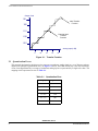
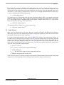
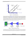
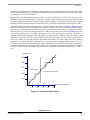
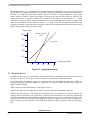
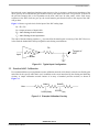
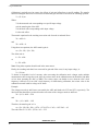
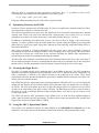
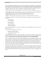
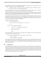
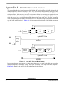
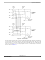
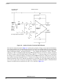
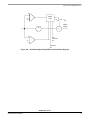
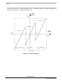
Freescale Semiconductor
Application Note
AN1947
Rev. 2, 08/2005
56F800 ADC
Understanding 56F800 ADC Specifications and
How to Get the Best Performance in Applications
Bill Hutchings
1.
Introduction
This document describes the meaning of the Data Sheet
specifications for the Analog-to-Digital Converter (ADC), how
they are calculated, and how they relate to real-world signal
impairments. In addition, this note introduces simple methods for
getting the best performance from the 56F800 ADC and gives an
overview of the differences in ADC performance for the various
56F800 components.
2.
Contents
1. Introduction ...........................................1
2. ADC Transfer Function and Error
Sources .............................................1
2.1
2.2
2.3
2.4
Quantization Error...........................2
Static Errors.....................................3
Dynamic Errors ...............................6
Measurement Methods ....................7
3. Using the 56F800 ADC .........................7
3.1
3.2
3.3
3.4
3.5
Input Impedance..............................7
Practical ADC Calibration ..............9
Optimizing Linearity and ENOB ..11
Choosing the Right Device ...........11
Using the ADC’s Operational
Modes ............................................11
4. Conclusion ..........................................13
ADC Transfer Function and Error
Sources
This section describes the ideal transfer function for an ADC. The
Data Sheet specifications provide data on how the real ADC
transfer function strays from the ideal.
The theoretical ideal transfer function for an ADC is a straight
line, but this would require an infinite number of steps, and
therefore an infinite number of bits to represent. A practical
theoretical transfer function is a uniform linear staircase function,
which is shown in Figure 2-1. The Data Sheet ADC
specifications describe in quantitative terms how far the
component deviates from the ideal transfer function.
© Freescale Semiconductor, Inc., 2004, 2005. All rights reserved.
A. 56F800 ADC Internal Structure ..........14
ADC Transfer Function and Error Sources
Output Code
101
Ideal Transfer
Function
100
011
Practical Ideal
Transfer
Function
010
001
5
4
3
2
1
Analog Input (LSB)
Figure 2-1. Transfer Function
2.1 Quantization Error
The practical ideal transfer function used to represent a continuous analog signal as a set of discrete staircase
digital codes introduces quantization error. As Figure 2-1 shows, the width of each step is one code increment,
or one Least Significant Bit, so a range of continuous analog inputs is represented by a single code value. The
mapping can be represented as seen in Table 2-1.
Table 2-1. Quantization Error
Analog input
Digital Code
4.5 - 5.5
101
3.5 - 4.5
100
2.5 - 3.5
011
1.5 - 2.5
010
0.5 - 1.5
001
0 - 0.5
000
56F800 ADC, Rev. 2
2
Freescale Semiconductor
Static Errors
If the value 001 represents the mid-point of the analog input range of 0.5 to 1.5, then the analog value 1.0 is
represented by 001 with no error. But since the analog value of 0.5 is also represented by the digital value 001,
the end points of the analog range represent the maximum error. In terms of bits, the maximum error can be
expressed as +1/2 bit for the 0.5 endpoint and -1/2 bit for the 1.5 endpoint. Maximum physical voltage error,
ev, can be calculated with the following equation:
ev = (1 LSB voltage range)/2
The voltage range of 1 LSB depends on the full-scale voltage range that the ADC is set to sample and the total
number of digital codes present. Analog-to-Digital converters are specified in the number of bits of resolution.
If “n” is the number of bits of resolution, then the total number of digital codes present is 2n, so the voltage
range represented by each bit vb can be expressed as:
vb = (Full scale voltage range)/2n
The maximum physical voltage error ev can be expressed as:
ev = (Full scale voltage range)/2n+1
2.2 Static Errors
Static errors are characterized by offset error, gain error, integral non-linearity and differential non-linearity.
While static errors can be fully characterized using non-varying input signals, they affect the conversion of all
input signals, whether they are static or dynamic.
Let us first examine gain and offset errors, shown by Figure 2-2. Looking at the actual transfer function, we
see a DC-bias error causing the zero crossing to occur at a point other than the origin. So, the analog input that
causes a zero code to be output in this example is 1.5 to 2.5 code instead of 0 to 0.5 code. This offset error is a
constant across the entire analog input range. We can see the gain error reflected in the diagram in that the
actual transfer function doesn’t have a 45 degree slope. The following equation describes the best-fit linear
regression of the actual ADC transfer function.
y = ( EGAIN x ) + VOFFSET
EGAIN
= Gain error value from the component Data Sheet
x = Actual analog input
VOFFSET
= DC input offset voltage from the component Data Sheet
y = Apparent analog input converted by ADC
These effects are linear over the input voltages and frequency and demonstrate that the actual analog input
voltage can be solved for and the effects of the gain errors and offset voltages can be removed.
56F800 ADC, Rev. 2
Freescale Semiconductor
3
ADC Transfer Function and Error Sources
Output Code
101
Practical Ideal
Transfer
Function
100
011
Actual Transfer
Function
010
001
5
4
3
2
1
Analog Input (LSB)
Figure 2-2. Gain and Offset Errors
In any given system, the conversion point of interest to an algorithm can be fairly far removed from the analog
input of the ADC, as illustrated in Figure 2-3. In these cases, gain and DC voltage offsets can be introduced
external to the ADC, so it is often important to take the entire system into account when analyzing the total
gain and offset errors. A calibration step may be required, depending on the specific requirements of the end
system. In the calibration, known precise and accurate signals are injected into the system and conversions are
performed. The actual results of the conversions are compared to the expected values and the error values for
gain and offset voltage can be determined. These errors can then be removed digitally in the processor or by
trimming the analog circuitry before the analog input into the processor ADC.
56F800 device
Buffering/
Isolation/Gain
stage
Buffering/
Isolation/Gain
stage
Signal of interest
Figure 2-3. System Gain and Offset Errors
The 56F800 devices have been characterized and most of the gain and offset errors have been removed by
internal compensation in the chip. Designers should analyze the gain and offset errors stated in the Data Sheet
for the device being implemented and the requirements for the algorithm they are to perform, because it is
56F800 ADC, Rev. 2
4
Freescale Semiconductor
Static Errors
possible that no adjustment is required for proper operation. If it is determined that the gain and offset errors
must be compensated for, this is a relatively straightforward proposition because these errors are linear, stable
over frequency, and easily characterized.
Integral (INL) and differential non-linearity (DNL) are errors introduced by all ADC units. They are quite
difficult to compensate and characterize. In general, a designer will need to determine the required linearity for
a particular algorithm and choose the system components accordingly. As with gain and offset errors, integral
and differential non-linearity errors can be introduced at any part of the system and are not limited to the ADC.
The integral and differential non-linearity errors are closely related to one another. As shown in Figure 2-4, the
width of each conversion step of the output code sequence is not the same. This non-uniformity in step width is
the source of the differential and integral non-linearity. The differential non-linearity is the difference in width
from the ideal case in each step and is measured in LSBs. In the specific case shown in Figure 2-4, the net
result of the non-linearities is an under-representation of the code sequences 011 and 101, which have a
negative differential non-linearity because the width is less than the ideal 1 LSB bit width. The sequence 100
will be over-represented and has a positive differential non-linearity because the step width is greater than 1
LSB. It is possible in some ADCs that the differential non-linearity will cause output codes to be missing
completely or repeated. An ADC’s Monotonicity is guaranteed when the digital output codes increase, or
remain the same, with increasing analog input voltage. Monotonicity is guaranteed in the 56F800 components.
A maximum differential non-linearity of one 1 LSB or less also ensures a monotonic transfer function with no
missing or repeated codes. All 56F800 components have a maximum differential non-linearity of 1 LSB or
less.
Output Code
101
100
011
Ideal Transfer
Non linear transfer function
010
001
5
4
3
2
1
Analog Input (LSB)
Figure 2-4. Non-linear Static Errors
56F800 ADC, Rev. 2
Freescale Semiconductor
5
ADC Transfer Function and Error Sources
Integral non-linearity is the summation of the previous differential non-linearity errors at any given point. In
the 56F800 devices, integral non-linearity is specified by using test equipment to determine the actual transfer
function of the ADC, then performing a linear regression to produce a best-fit straight line for the actual
transfer function. When the integral non-linearity is measured, the gain and offset errors are nullified. The
integral non-linearity is specified in LSBs of the conversion code outputs, so a specification of +/- 3 LSBs
means that at any given analog input, the summation of previous differential errors produces an output code
where the error from the ideal is within the range of +/- 3 output codes. The maximum specification for the
integral non-linearity is the point of greatest distance of the best-fit straight line transfer function from the ideal
transfer function and is again expressed in LSBs.
Output Code
101
Real best fit transfer
function
100
Ideal Transfer
011
010
001
5
4
3
2
1
Analog Input (LSB)
Figure 2-5. Integral Non-linearity
2.3 Dynamic Errors
In addition to the static error specifications, other specifications are commonly given that take into account
dynamic error sources. This section reviews a few that are specified in the 56F800 Data Sheets.
In the Data Sheet, the dynamic errors are characterized by the Total Harmonic Distortion (THD), the
Signal-to-Noise plus Distortion (SINAD), the Spurious Free Dynamic Range (SFDR), and the Effective
Number Of Bits (ENOB).
THD is the rms power in the harmonics of the signal of interest.
SINAD is the ratio of the rms signal power to the noise floor power plus the harmonic distortion.
SFDR is the decibel distance of the largest spur or harmonic noise in comparison to the signal of interest. For
example, in the measurement of the specification, a signal is injected into the ADC at a frequency of 8KHz and
a Fourier transformation is performed on the samples to yield the energy level as a function of frequency. The
signal of interest will form the largest decibel (dB) spike. Below this will be a noise floor with several spikes or
spurs occurring at specific frequencies. The SFDR is the distance in dB of the signal of interest to the largest
spur.
56F800 ADC, Rev. 2
6
Freescale Semiconductor
Input Impedance
A good overall figure of merit that takes into account the effects of the overall noise and the distortion of the
signal is the Effective Number Of Bits, or ENOB. The ENOB takes into account the noise floor of the
component and reflects the best achievable dynamic accuracy of the ADC. The ENOB reflects the best-case
achievable noise-free number of bits. The ENOB number specifically does not include the static gain, offset,
and linearity errors.
The dynamic range of an ADC refers to the decibel ratio of the smallest to the largest value that can be
represented. The dynamic range of an ADC is fully dependent on the bits of resolution. The following equation
calculates the dynamic range of an ADC:
Dynamic Range = 20log10(2n)
“n” is the number of bits of resolution
2.4 Measurement Methods
Each 56F800 component’s ADC is characterized, in accordance with IEEE Std 1241-2000, for gain, offset,
DNL, INL, SNR, THD, SFDR, SINAD and ENOB.
The Gain, offset, INL and DNL are performed using the code density method, which uses a noise-free sine
wave. Gain and offset are calculated doing a least-squared fit from the histogram data obtained from the
digitized sine wave.
3.
Using the 56F800 ADC
This section explores some of the issues that must be considered to get the best performance from the ADC in
your system and how to choose an appropriate 56F800 component in terms of ADC performance.
3.1 Input Impedance
An equivalent circuit for an analog input is shown in Figure 3-1.
ADC analog input
1
3
2
4
Figure 3-1. Equivalent Analog Input Circuit
1. Parasitic capacitance due to package, pin-to-pin, and pin-to-package base coupling. . . . . . . 1.8pf
2. Parasitic capacitance due to the chip bond pad, ESD protection devices and signal routing. 2.04pf
3. Equivalent resistance for the ESD isolation resistor and the channel select mux.. . . . . . . 500 ohms
4. Sampling capacitor at the sample and hold circuit. . . . . . . . . . . . . . . . . . . . . . . . . . . . . . . . . . . 1pf
56F800 ADC, Rev. 2
Freescale Semiconductor
7
Using the 56F800 ADC
When interfacing to the ADC, one must be concerned with the ADC clock rate and the size of the sampling
capacitor, which is 1pf and depicted in Figure 3-1 as “4”. This capacitor is charged to the sampling voltage and
discharged to VDD / 2 during each ADC clock cycle. This effectively creates a switched cap implementation of
a resistor that is dependent on clock rate and voltage level at the input. This switched cap equivalent resistance
is effectively the input impedance to the ADC. The equivalent circuit shown in Figure 3-1 is valid for realistic
operating conditions and ADC clock rates. The circuit in Figure 3-1 is present at any specific analog input
during the time that the analog input is being converted and the analog mux is feeding the input into the
appropriate sample and hold circuitry. During periods when another input is being muxed into the sample and
hold circuitry and converted, or if no conversion occurs, the external circuitry will see a very high input
resistance at the analog input pin. As an example, if the input voltage is 1 volt greater than VREF / 2 and the
ADC clock rate is 5 MHz, then the ADC input impedance is:
i = C dv/dt, so
i dt = C dv
Where:
dt = 1/5e+6
dv = 1 volt
C = 1e-12
So:
i = (5e+6) (1e-12) (1) = 5e-6
R = V/I
So:
R = 1 / 5e-6 = 200K ohms
The input impedance at the ADC clock rate of 5MHz can be as low as 200K ohms A typical input
configuration for driving the ADC is depicted in Figure 3-2. Using this input configuration, if one wants to
maintain the signal amplitude to within 10 bits or more of its original amplitude, at the anti-aliasing capacitor
Ca, then the source impedance of what's driving the ADC must be less than:
Rs / (Rs + Ri) = 1 / (2+10)
Source resistance of the driver = Rs
Input resistance of the ADC = Ri
Where:
Ri = 200K ohms
1 / (2+10) = .0009766
Solving for Rs results in:
Rs = 200 ohms
If the ADC clock rate were changed to 1MHz, then the source impedance of what's driving the ADC must be
less than 1K ohms to maintain an effective input signal that's within 10 bit of its original amplitude.
56F800 ADC, Rev. 2
8
Freescale Semiconductor
Practical ADC Calibration
Increasing the source impedance introduces gain error, not a loss, in accuracy. As the source impedance of the
driver goes up, the overall transfer gain from the buffer to the output of the ADC will go down. As shown in
the previous example, this is also dependent on the ADC clock rate. In other words, with a fixed source
resistance as the ADC clock rate goes up, the overall transfer gain from the buffer to the output of the ADC
will go down.
Figure 3-2 shows a typical circuit for the input of the ADC analog input.
Rs = Ro + Ra
Ro= Output resistance of input buffer
Ra= Anti-aliasing circuit resistance
Ca= Anti-aliasing circuit capacitance
The value of the anti-aliasing capacitor, Ca, does not affect the transfer gain or accuracy of the ADC. However,
it does limit the bandwidth of the input signal for anti-aliasing considerations.
Ra
Input
To input of
ADC
Ro
Ca
Buffer
Figure 3-2. Typical Input Configuration
3.2 Practical ADC Calibration
It's recommended that a user implements an auto-calibration network on his board, so that he can find the gain
and offset for the specific ADC that's used, in addition to the errors introduced by the aliasing and buffering
circuitry. A simple calibration network consists of an array of matched precision resistors, as shown in
Figure 3-3.
Node A
Node B
0.6666(VREF)
0.3333(VREF)
VREF
Figure 3-3. Example Calibration Circuitry
56F800 ADC, Rev. 2
Freescale Semiconductor
9
Using the 56F800 ADC
Calibration is typically used to remove the effects of gain and offset from a specific reading. The transfer
function relating an ideal code to a measured code that has gain and offset is shown in the following equation:
Y = (X - b)/m
Where:
Y is the measured code corresponding to a specific input voltage
m is the transfer gain of the ADC
X is the ideal code corresponding to this input voltage
b is the code offset.
The transfer equations for the resulting conversion code for node A and node B are:
Ya = mXa +b
and
Yb = mXb + b
Using these two equations, the ADC transfer gain is:
m = (Ya - Yb) / (Xa - Xb)
The offset code is:
b = Ya - mXa
or
b = Yb - mXb
Note: Using either equation should result in the same answer.
Finally, the resulting code that's been corrected for gain and offset error, for any input voltage, is:
X = (Y-b)/m
To obtain an acceptable level of accuracy when converting the calibration node voltages, make multiple
measurements, then average the result. Also, the resistor values in the calibration network should be 200 ohms
or less when operating the ADC at 5MHz. The resistor values can double in size when the ADC clock
frequency is halved, so for an ADC clock frequency of 1MHz during calibration, the resistor value in the
calibration network could be as large as 1K ohms.
Example:
The voltages at nodes A and B were converted by the ADC and found to be 2570 and 1273, respectively. The
ideal codes that should have resulted from the conversion of the voltage at nodes A and B are:
Xa = (2/3) * 4095 = 2730
and
Xb = (1/3) * 4095 = 1365
Therefore, the transfer gain "m" is:
m = (Ya - Yb)/(Xa - Xb) = (2570 - 1273)/(2730 - 1365) = 1297/1365 = .95
The code offset "b" is: 2570 - (2730) * .95 = -23.5
56F800 ADC, Rev. 2
10
Freescale Semiconductor
Using the ADC’s Operational Modes
When this ADC is converting an input signal that's at mid-scale, VREF / 2, it produces a code of 1922.
Correcting this result using the offset and gain derived previously yields:
X = (Y - b)/m = (1922 - (-23.5))/.95 = 2048
Using this calibration method corrects for the effects of gain and offset.
3.3 Optimizing Linearity and ENOB
In order to achieve optimal results in ENOB terms, all sources of coupled noise should be minimized. These
can be from sources internal or external to the chip.
The ADC has operational sweet spots where the digital noise from its internal environment has a minimal
coupling effect. These sweet spots occur when the ADC clock prescaler is set to values of 4, 9 or 14. If not
operating at one of these sweet spots, the accuracy of the ADC typically drops by 1/2 of a bit.
In addition to minimizing the internal noise sources, care must be taken in design of the external noise
coupling. To achieve optimal results, the board should have separate analog and digital power and ground
planes and very clean VREF signals. Using these methods, the best practically achievable ENOB will be as
stated in the Data Sheet.
Since noise is modeled as a Gaussian distribution, the noise power can be lowered through a scheme of
oversampling the input and averaging the samples. In the averaging process, noise spikes will tend to cancel
each other out, lowering the overall noise power and thus increasing the ENOB. SNR improvement is
proportional to the amount oversampling and averaging performed.
The INL peaks at the minimum or maximum codes and is minimized between the 10% to 90% code range. If
the user wishes to maximize accuracy, he should limit the input swing to be within the 10% to 90% range from
ground to VREF. The INL measurement in the Data Sheets is measured using the 10% to 90% range.
3.4 Choosing the Right Device
The ADC is a System-on-Chip (SoC) peripheral that is on the IPBus of the chip. The ADC peripheral is
identical in all 56F800 components, but the performance of the ADC is different across the components. The
ADC’s performance is affected by the physical location of the peripheral in the silicon. These layout
considerations affect the amount of coupled noise and resistive loads that directly impact the noise figures, DC
offsets, gain errors, and the linearity.
The 56F803/805/807 have significantly better performance than the 56F801/802. So if you are considering the
56F801/802, but find they do not have the required ADC performance, then you should move your design to
the 56F803. The ADC performance in the areas of gain and voltage offsets was improved over the various
revisions of the components as the ADC circuitry was tuned. The Data Sheets specify the current revision of
the silicon, so if you see markedly different voltage and gain offsets, verify that you are do not have an old
revision of the silicon.
The 56F827 has the best ADC performance of the 56F800 series. Its ADC has been modified slightly to
achieve gains in linearity and noise performance. To achieve these results, the maximum ADC internal clock
frequency has been lowered from 5MHz to 2.5MHz.
3.5 Using the ADC’s Operational Modes
This section is not intended to replace the data published in the DSP56F800 User Manual, but to add
clarification. The reader must use the information located in the manual to fully understand this section.
56F800 ADC, Rev. 2
Freescale Semiconductor
11
Using the 56F800 ADC
First, consider samples in the ADC and how they relate to the scan modes. ADC Inputs can be configured for
either single-ended or differential mode and a user can mix single-ended and differential inputs. Samples may
be taken either one at a time (sequential mode) or two at a time (simultaneous mode). The mapping of input pin
to sample number is arbitrary, with one exception: the same input pin cannot be used for both sides of a
simultaneous sample pair. For example: AN2/AN5 is a valid sample pair, but not AN2/AN2.
The ADC captures/converts up to eight samples at a time in a "scan". There are several different scan modes:
1) Once (single): The ADC starts to sample just one time using the START bit or by a sync pulse. This mode
must be re-armed by writing to the ADCR1 register again before capturing another scan.
2) Triggered: Sampling begins with every recognized START command or sync pulse
3) Loop: The ADC continuously take samples as long as power is on and the STOP bit has not been set.
Each of the preceding sequences can be coupled with sequential or simultaneous modes, enabling a total of six
scan modes:
•
Once Sequential
•
Once Simultaneous
•
Loop Sequential
•
Loop Simultaneous
•
Triggered Sequential
•
Triggered Simultaneous
One of these six configurations is coded in the ADC Mode Control bits (SMODE[2:0]) of the ADC Control
Register 1 (ADCR1).
The scan modes can be triggered in several ways:
•
Directly under software control
•
By the output of a quadrature timer
•
By a PWM reload event
The PWM reload event is first routed through a Quadrature Timer that can be used to provide an arbitrary
delay before causing the ADC convert command. This is discussed in greater detail in application note
AN1933, Synchronization of on-Chip Analog-to-Digital Converter on DSP56F80x DSPs.
To set up a periodic conversion at a specific rate, the triggered mode can be used in conjunction with one of the
timers to provide the conversion start or sync pulse. An interrupt can be generated at the conclusion of the
conversion. At this point, the samples can be and should be read from the ADC result registers. These registers
are not buffered, so the samples must be read before the next conversion writes out to the result registers.
The ADC can also be set up in a continuous loop mode, where a trigger to start conversion is not required. But
the end of conversion cannot be set to cause an interrupt in this mode, so the software must poll the ADC status
register to know when the conversion has been completed.
Because the ADC peripheral has an internal pipeline, the first conversion requires 8.5 ADC clock cycles and
each additional conversion requires 6 ADC clock cycles. The 2.5 clock cycle difference is the time required to
fill the pipeline. In the triggered modes or the once mode, the pipeline must be filled whenever a sync pulse or
START command is issued. In the loop mode, the pipeline is filled only once at the very beginning of the
process.
56F800 ADC, Rev. 2
12
Freescale Semiconductor
Using the ADC’s Operational Modes
For example, the ADC is set up in sequential triggered mode with only the first four samples enabled. The
number of clock cycles required for the conversion follows:
Nclk = (Sample0 conversion) + (Sample1 conversion) + (Sample2 conversion) + (Sample3 conversion)
= (8.5) + (6.0) + (6.0) + (6.0) = 26.5 ADC clock cycles
The samples which are not to be converted must be disabled in the ADC sample disable register. Any samples
that are not disabled will be converted and will add to the total ADC conversion time.
The ADC conversion time calculated previously is only the amount of time the ADC requires to perform the
conversion. But in a real system, the samples must be removed from the result registers using software,
typically run from an ISR associated with the end of conversion interrupt.
As an example of this constraint, assume a system running on a 56F800 component, with the ADC in a
simultaneous triggered mode using a timer set to provide start pulses at a 100k sample rate (10µs interval), the
ADC clock set for 5MHz; the processor running at 40 MIPS from internal Flash; and an ISR at the end of
conversion interrupt takes the samples and buffers them.
The time to perform the conversion is:
Tconv = Time to perform conversion
= (8.5 ADC clock cycles) * (time per cycle) = (8.5) * (0.2e-6)
= 1.7µs
Tget samples = Time available to get samples
= Ttrig rate- Tconv + (Time for 6 ADC clock cycles)
= 10µs - 1.7µs + (6 * 0.2e-6)
= 10µs - 1.7µs + 1.2µs
= 9.5µs
At the beginning of the second conversion, the result registers still contain the previous data, which will not be
overwritten for at least 6 ADC clock cycles.
Ninstr = Number of instructions cycles left for software to retrieve samples
= (Tget samples) / (Tinstr)
= 9.5µs / (1 / 40MHz) = 380 instructions
This example indicates that for high sampling rates, the processor may have difficulty keeping up with the
ADC samples, especially if there is a significant processing load in handling this data and/or there are other
peripherals that must also be serviced. A thorough system analysis is recommended to make sure real-time
issues are not encountered.
4.
Conclusion
The 56F800 family includes parts with a very powerful and accurate on-board ADC peripheral. This document
has discussed in detail the Data Sheet parameters, what they measure, and how they are measured. It has
discussed at a high level the performance characteristics across the family of components, but the reader should
consult the Data Sheet for the component being implemented to find the latest performance characteristics.
Additionally, it has explored ways to achieve optimal performance out of the ADC, as well as some of the
modes of operation and performance items to consider.
56F800 ADC, Rev. 2
Freescale Semiconductor
13
Conclusion
Appendix A
56F800 ADC Internal Structure
This appendix describes the internal structure of the 56F800 ADC peripheral. The cyclic ADC designed for the
56F800 components consists of a dual-cyclic ADC core, dual interface function and an analog input select
mux. The input select mux routes the analog inputs of choice to either ADC#1 or ADC#2. While in the
simultaneous mode, both converters are used in a synchronous fashion for converting two signals at the same
time. The interface function that follows the input select mux samples the single-ended or differential input
signal and converts it to a scaled differential within the operational range of the ADC. The ADC coreconsists
of two Redundant Signed Digit (RSD) sections that resolve one bit of the Analog-to-Digital conversion during
each half ADC sample clock cycle. Figure A-1 depicts a top-level block diagram of the 56F800 components’
cyclic converter.
Interface
Function
Mux
RSD#1
θ1
θ2
Cyclic ADC Core
AN0
AN7
RSD#2
Analog
Input
Select
Mux
ADC#1
Interface
Function
Mux
RSD#1
θ1
RSD#2
θ2
Cyclic ADC Core
ADC#2
Figure A-1. Cyclic ADC Top-Level Block Diagram
In most general-purpose applications, the analog signal that’s to be converted by the ADC can have values
ranging from ground to the supply voltage. This signal is selected via the input select mux, depicted in
Figure A-2, sampled by the interface function and presented to the ADC core.
56F800 ADC, Rev. 2
14
Freescale Semiconductor
Using the ADC’s Operational Modes
Swap
Select
Channel
Select
AN0
To Interface
Function
ADC #0
AN1
AN2
AN3
VREF / 2
Swap
Select
Single-ended
Differential
Channel
Select
AN4
To Interface
Function
ADC #1
AN5
AN6
AN7
VREF / 2
Single-ended
Differential
Figure A-2. Input Select Mux
For noise isolation reasons, the ADC core in turn uses differential signaling that’s within the operational range
of its sub-functions, which is less than the supply voltage and more than ground potential. The purpose of the
interface functions is to convert the full range, single-ended or differential signal, into a scaled differential
signal during the sampling process of Analog-to-Digital conversion. A functional diagram of the interface
function is depicted in Figure A-3.
56F800 ADC, Rev. 2
Freescale Semiconductor
15
Conclusion
interface function
input select mux
equivalent ckt
θ2
C3
analog
input
pad
500
θ2
C1
1pf
3.8pf
parasitic
pad &
pkg cap
θ1
θ2
θ2
1pf
C2
θ1
amp pos
output
amp neg
input
Out_Pos
Differential
Amplifier
VDD / 2
VREF / 2
(for single-ended conversions)
θ1
amp neg
output
amp pos
input
Out_Neg
θ2
VDD / 2
C4
θ2
Figure A-3. Interface Function Functional Block Diagram
The interface function depicted in Figure A-3 works on the principle of charge conservation and distribution.
The switches labeled θ2 are closed during the first half of a clock cycle and those labeled θ1 are closed during
the second half of a clock cycle. Also, all capacitors are of the same size, typically in the picofarad range. For a
single-ended signal, during θ2, the input signal and VREF / 2 are sampled onto capacitors C1 and C2. During θ1,
capacitors C1 and C2 are shorted together and charge is redistributed between C1 and C2 so that the voltage on
C1 and C2 becomes equal. If the input signal were larger than VREF / 2, then the voltage on C1 is reduced and
the voltage on C2 is increased during θ1. In response to this charge movement, the voltage at Out_Pos moves
up to replace the charge being taken from C1. Likewise, the voltage at Out_Neg moves down to negate the
charge increase that occurs on C2. Because all capacitors are of the same size, the voltage change that occurred
at C1 and C2 is the same at Out_Pos and Out_Neg, resulting in a differential signal. A functional block
diagram of an RSD function contained in the ADC core is depicted in Figure A-4.
56F800 ADC, Rev. 2
16
Freescale Semiconductor
Using the ADC’s Operational Modes
+
Vh
Digital
Logic
-
+ VREF, 0, or - VREF
+
2X
+
Vl
residue
voltage
error
correction
bit
-
extracted
bit
Figure A-4. Redundant Signed Digit, RSD Functional Block Diagram
56F800 ADC, Rev. 2
Freescale Semiconductor
17
Conclusion
The detailed description of how the RSD stage works can be found in reference manuals addressing the
functionality of the cyclic Analog-to-Digital converter. A Robertson diagram, depicting the voltage in to
residue out and data bits out, is depicted in Figure A-5.
residue
voltage
VREF
dout = 1, 0
dout = 0, 1
dout = 0, 0
- VREF
VH
VL
input
voltage
VREF
VRES = 2VIN + VREF
VRES = 2VIN
VRES = 2VIN - VREF
- VREF
Figure A-5. Robertson Diagram
56F800 ADC, Rev. 2
18
Freescale Semiconductor
Using the ADC’s Operational Modes
Once the chosen analog signals have been selected, the ADC conversion starts with the sync signal going high,
as depicted in Figure A-6. The input signals to be converted are sampled onto capacitors C1 and C2, shown in
Figure A-3, during θ2 in preparation for conversion during θ1. During θ1, the sampled signals are converted to
scaled differential signals and passed into the first RSD block, shown in Figure A-1, where a data bit is
extracted and its capacitors are charged in preparation for calculating the residue. The residue from the first
RSD stage is then calculated on θ2 and passed into the second RSD stage, where another data bit is extracted
and its capacitors are charged in preparation for calculating the residue. The residue, in the second stage, is
then calculated and passed back into the first RSD stage, during θ1, where another bit is extracted and
preparations are made for calculating the residue. The resulting residue continues to be passed back and forth
between the two RSD stages until the required number of bits have been extracted. The signaling diagram,
shown in Figure A-6, is for a 12-bit extraction.
Both ADCs sample their
input signals on the first full
phase 2 prior to the start of
ADC conversion
ADC Clock
ADC conversion starts on
the first full phase 1
following the rise of the
sync signal.
θ2 θ1 θ2 θ1 θ2 θ1 θ2 θ1 θ2 θ1 θ2 θ1 θ2 θ1 θ2 θ1 θ2 θ1
Sync
Translation
Phase
RSD Phase
Data rdy
Figure A-6. ADC Signaling
56F800 ADC, Rev. 2
Freescale Semiconductor
19
How to Reach Us:
Home Page:
www.freescale.com
E-mail:
[email protected]
USA/Europe or Locations Not Listed:
Freescale Semiconductor
Technical Information Center, CH370
1300 N. Alma School Road
Chandler, Arizona 85224
+1-800-521-6274 or +1-480-768-2130
[email protected]
Europe, Middle East, and Africa:
Freescale Halbleiter Deutschland GmbH
Technical Information Center
Schatzbogen 7
81829 Muenchen, Germany
+44 1296 380 456 (English)
+46 8 52200080 (English)
+49 89 92103 559 (German)
+33 1 69 35 48 48 (French)
[email protected]
Japan:
Freescale Semiconductor Japan Ltd.
Headquarters
ARCO Tower 15F
1-8-1, Shimo-Meguro, Meguro-ku,
Tokyo 153-0064, Japan
0120 191014 or +81 3 5437 9125
[email protected]
Asia/Pacific:
Freescale Semiconductor Hong Kong Ltd.
Technical Information Center
2 Dai King Street
Tai Po Industrial Estate
Tai Po, N.T., Hong Kong
+800 2666 8080
[email protected]
For Literature Requests Only:
Freescale Semiconductor Literature Distribution Center
P.O. Box 5405
Denver, Colorado 80217
1-800-441-2447 or 303-675-2140
Fax: 303-675-2150
[email protected]
Information in this document is provided solely to enable system and
software implementers to use Freescale Semiconductor products. There are
no express or implied copyright licenses granted hereunder to design or
fabricate any integrated circuits or integrated circuits based on the
information in this document.
Freescale Semiconductor reserves the right to make changes without further
notice to any products herein. Freescale Semiconductor makes no warranty,
representation or guarantee regarding the suitability of its products for any
particular purpose, nor does Freescale Semiconductor assume any liability
arising out of the application or use of any product or circuit, and specifically
disclaims any and all liability, including without limitation consequential or
incidental damages. “Typical” parameters that may be provided in Freescale
Semiconductor data sheets and/or specifications can and do vary in different
applications and actual performance may vary over time. All operating
parameters, including “Typicals”, must be validated for each customer
application by customer’s technical experts. Freescale Semiconductor does
not convey any license under its patent rights nor the rights of others.
Freescale Semiconductor products are not designed, intended, or authorized
for use as components in systems intended for surgical implant into the body,
or other applications intended to support or sustain life, or for any other
application in which the failure of the Freescale Semiconductor product could
create a situation where personal injury or death may occur. Should Buyer
purchase or use Freescale Semiconductor products for any such unintended
or unauthorized application, Buyer shall indemnify and hold Freescale
Semiconductor and its officers, employees, subsidiaries, affiliates, and
distributors harmless against all claims, costs, damages, and expenses, and
reasonable attorney fees arising out of, directly or indirectly, any claim of
personal injury or death associated with such unintended or unauthorized
use, even if such claim alleges that Freescale Semiconductor was negligent
regarding the design or manufacture of the part.
Freescale™ and the Freescale logo are trademarks of Freescale Semiconductor,
Inc. All other product or service names are the property of their respective owners.
This product incorporates SuperFlash® technology licensed from SST.
© Freescale Semiconductor, Inc. 2004, 2005. All rights reserved.
AN1947
Rev. 2
08/2005