1
US007757029B2
(12) United States Patent
(10) Patent No.:
Bonnet
(54)
US 7,757,029 B2
(45) Date of Patent:
ON THE FLY CONFIGURATION OF
(58)
Jul. 13, 2010
Field of Classi?cation Search ....... .. 710/3014302;
ELECTRONIC DEVICE WITH ATTACHABLE
714/726, 727, 728, 729; 324/757, 763; 702/117,
SUB-MODULES
(75) Inventor:
702/1 18
See application ?le for complete search history.
(56)
References Cited
Thierry Jean Claude Andre Bonnet,
Geneva (CH)
U.S. PATENT DOCUMENTS
(73)
Assignee: sT'Ericsson SA’ plan'les'ouates (CH)
( * ) Notice:
4,135,240 A *
1/1979 Ritchie ..................... .. 711/164
Subject to any disclaimer, the term of this
(Continued)
patent is extended or adjusted under 35
FOREIGN PATENT DOCUMENTS
U.S.C. 154(b) by 572 days.
JP
(21) APP1-NO-I
10/492,566
(22)
Oct 14 2002
PCT Filed
'
l
07-98686 A
4/1995
OTHER PUBLICATIONS
IEEE, Inc. IEEE Standard for a Mixed-Signal Test Bus. Jun. 26,
’
1999.*
(Continued)
(86)
PCT NO':
§ 371 (0X1)
’
(2), (4) Date:
(87)
PCT/IB02/04229
Primary ExamineriMark Rinehart
Assistant ExamineriMattheW D Spittle
Apr. 14, 2004
(Grgup PLLeé g
74 Allorn ,A enl, orFirmiRobert lannucci; Seed IP Law
(57)
PCT Pub. No.: WO03/034202
ABSTRACT
Electronic device (10) comprising a control unit (11), a p1u
PCT Pub. Date: Apr. 24, 2003
(65)
Prior Publication Data
Us 2006/0090109 A1
unit (11) With those sub-modules (12, 13) that are attached/
connected to the slots (15). The control unit (11) is capable of
issuing commands in order to put the sub-modules (12, 13) in
Apr' 27’ 2006
.
(30)
rality of slots (15) for attaching/ connecting sub-modules (12,
13), and means (15, 16, 17) for interconnecting the control
.
.
.
.
a by-pass mode, to read identi?cation information from sub
Forelgn Apphcatlon Prmnty Data
Oct. 17, 2001
(EP)
modules (12, 13), Write parameters into and/or read param
................................ .. 01124735
eters from at least one of the sub-modules (12, 13), and to
re-check Whether the con?guration of the electronic device
(51) Int. Cl.
H05K 7/10
(52)
(10) has changed by adding or removing a sub-module (12,
13).
(2006.01)
US. Cl. ..................... .. 710/301; 710/302; 714/727;
324/763; 702/117; 702/118
7 Claims, 6 Drawing Sheets
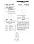
fig
‘51D
12
5
D
Slave JTAG controller
O
1 1 '-\ T Control
Processor
0,
JTAG
TDl m0
emp'ly slot
20
empty slot
1 9 "-\
q
_
16
~/~15
~/~15
15
|
n
a 1
Main board
K
n
>
l
>
\A
\TAP
connections
\Applicatlon connection
I
l
17
18
14
US 7,757,029 B2
Page 2
U.S. PATENT DOCUMENTS
5,132,635 A *
7/1992
5,325,368 A
6/1994 James et al.
5,544,309 A *
5,572,141 A *
6,901,344 B2 *
5/2005
Mantey et a1. ............ .. 702/122
6,975,752 B2 *
12/2005
Dixon et al. .............. .. 382/132
Kennedy .................. .. 324/763
8/1996 Chang et a1. ................ .. 714/30
11/1996 Hutton ........ ..
OTHER PUBLICATIONS
Sun Microelectronics. microSPARC-llepilntroduction to JTAG
5,584,030 A * 12/1996 Husak et a1.
5,617,081 A * 4/1997 Madnick et al.
Boundary Scan. White Paper. Jan. 1997.*
IEEE. IEEE Standard Test Access Port and Boundary-Scan Archi
5,617,430 A *
tecture. 2001.*
5,852,617 A
5,898,704 A
5,935,228 A
4/1997 Angelotti et al. .......... .. 714/726
12/ 1998 Mote, Jr.
4/1999 Kawano
8/1999 Shinomura
Domain Technologies. ZSP-USB-JTAG Emulator. Users Guide. Ver
sion 2.3. Jul. 2007.*
Digilent. Digilent Adept Suite. User’s Manual. Nov. 30, 2006*
6,000,051 A
12/ 1999 Nadeall-Dostie et a1
Altera. Using Command-Line Jam STAPL Solution for Device Pro
6,311,242 B1 *
6,353,905 B1 *
10/2001 Falkenburg 6t {11. ....... .. 710/301
3/2002 Noguchi ................... .. 714/728
gfamming, Application Note 425, Version 11, Dec, 2006*
Cousineau et 31‘, “Design Ofa JTAG Based Run Time Recon?gurable
6,363,452 B1
3/2002 Lach
6,522,985 B1 *
2/2003
6,529,987 B1
3/2003 Reid
System,” IEEE Comput. Soc., Los Alamitos, CA, 1999, 2 pgs.
Swoboda et al. .......... .. 702/117
* cited by examiner
US. Patent
Jul. 13, 2010
Sheet 1 of6
US 7,757,029 B2
10
H %12
8
f
g
1 1 “\p COI'IUOI
n5
Processor
a
Slave JTAG controller
JI'AG
rnrmo
20
empty slot
~/~15
15
M
k
:
\TAP
7
‘A14
connections
Mainboard
\Application connection
I
l
17
18
Frg .1
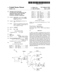
New sub-module
gD
13 ;1D M12
l e,5
11'-\- Control
eob
Processor
5;
3
MASTER JTAG
JTAG
20 JTAG
CONTROLLER
m we
Tm mo
~/~15
I
I I
=
M
~1~15
M
=
'
Board
empty slot
>
~/~15
M
TAP
‘A14
onnections
\Application connections lines
Fig.2
US. Patent
Jul. 13, 2010
Sheet 2 0f 6
US 7,757,029 B2
E
TDO
21-»
TDl
g
T575]
I BVPassr99%ister
27
28
|
MuxCm
Decode
——T__>|
TMS
TRST_N
2o
IR
——> TAPC
-
\
2:2
'
I
\
213
Ctrl: Control lines
Fig.3
US. Patent
Jul. 13, 2010
Sheet 3 of6
US 7,757,029 B2
Test logic ‘
reset
6 1"
0
Run test
1
Idle
‘
A
>
Select DR
1
>
scan
1
Select IR
scan
lo
Capture DR
1
‘0
Capture IR
I0
_>
I°
Shift DR
0
->
Shift IR
I1 0
p
0
1
ExitI DR
0
I1 0
n
ExitI IR
I0
Pause DR
0
1 O 0
I
Ex|t2 IR
II
I0
Pause IR
0
I1 O
Updafte DR
Update IR
11
o
Fig.4
Ex1t2 IR
II
1
0
US. Patent
Jul. 13, 2010
Sheet 4 of6
US 7,757,029 B2
19
11
(
1
1
I
Program & Data
memory
I
|
Application
30
F TCK >
'
‘g
TMS >
5
TDO
TAP
LU
>
A
TRST_N ’ Connector
5
TDI
D. .‘_...—._..
MICROPROCESSOR
31
—-
_ P29
JTAG MASTER
CONTROLLER
CONTROL PROCESSOR
Fig.5
US 7,757,029 B2
1
2
ON THE FLY CONFIGURATION OF
ELECTRONIC DEVICE WITH ATTACHABLE
SUB-MODULES
nected to the slots. The control unit is capable of issuing
commands in order to put the sub -modules in a by-pass mode,
to read identi?cation information from sub-modules, to Write
parameters into and/or read parameters from at least one of
The present invention concerns the automatic con?gura
the sub-modules, and to re-check Whether the con?guration
of the electronic device has changed by adding or removing a
sub-module.
Other advantages of the present invention are addressed in
connection With the detailed embodiments.
For a more complete description of the present invention
and for further objects and advantages thereof, reference is
made to the folloWing description, taken in conjunction With
tion of electronic devices Which can be extended or modi?ed
by attaching sub-modules. In particular, portable electronic
devices are concerned.
There are many electronic devices that can be extended,
modi?ed, or adapted according to needs by attaching sub
modules. In particular handheld devices and consumer
devices could be made more attractive When offering the
option to expand a basic system or When enabling the user to
add features that go beyond What the device offers in its basic
the accompanying draWings, in Which:
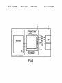
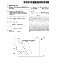
FIG. 1 is a schematic diagram of an electronic device,
con?guration.
according to the present invention, comprising one sub -mod
A handheld phone, eg a GSM phone, can for example be
ule and tWo empty slots.
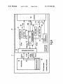
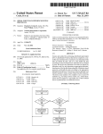
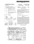
FIG. 2 is a schematic diagram of an electronic device,
modi?ed by alloWing to add an MP3 feature or a radio tuner,
just to give tWo examples. Most personal digital assistants
according to the present invention, comprising tWo sub-mod
(PDAs) have very small keyboards. If it Would be possible to
attach a larger keyboard When needed, the PDA could almost
be used like a regular personal computer. One could likeWise
ules and one empty slot.
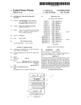
FIG. 3 is a schematic block diagram of a JTAG slave used
20
in sub-module, according to the present invention.
add multimedia capabilities by alloWing to attach a camera, or
FIG. 4 is a schematic representation of a state machine as
some speakers, for example.
A key issue is the re-con?guration that becomes necessary
used in the control processor of a slave processor, according
to the present invention.
FIG. 5 is a schematic block diagram of control processor
Whenever a sub-module is plugged in or removed. The recon
25
implemented With a microprocessor, according to the present
?guration has to be straightforward and reliable so that it can
be carried out by the user Without having to read a manual
?rst. Some personal computers and similar systems have
What is called a plug-and-play feature. Plug-and-play basi
cally means that a module (e.g., a PCI adapter card, peripheral
device or the like) can be plugged in Without having to Worry
about hardware and software con?guration issues. The com
invention.
FIG. 6 is a schematic block diagram of control processor
30
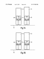
FIG. 7A, 7B is a schematic representation of tWo steps,
according to the present invention.
The expression electronic device in the present context is
meant to include devices such as: personal digital assistants
puter is able to detect a neW module and to automatically
embed it in the given environment.
JTAG is a protocol that is speci?cally designed andused for
integrated circuit (IC) or board testing. Details of JTAG are
implemented With dedicated hardWare, according to the
present invention.
35
(PDAs), cellular phones, computing terminals, handheld
computers, cameras, multi-media devices, consumer devices,
DECT devices, etc. This listing is not meant to be exhaustive.
de?ned in the IEEE standard 1 149.1-1990. Basically, a JTAG
implementation comprises a JTAG-master (also called JTAG
Examples of sub-modules are: a GSM/UMTS modem, a
controller) and at least one JTAG slave. The JTAG master
issues JTAG instructions to control and test the J TAG slave.
To the best of our knoWledge, there are currently no pro
MP3 player, a FM radio, a PDA, a color display, a keyboard,
etc. This listing is not meant to be exhaustive.
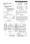
An electronic device 10 in accordance With the present
invention comprises a main control processor 11 and several
attachable/detachable sub-modules 12, 13, as illustrated in
FIGS. 1 and 2. The main board 14 of the electronic device 10
comprises connectors 15, or the like, Which alloW the sub
modules 12, 13 to be attached and detached. There is a bus
40
tocols for automated con?guration of electronic devices With
insertable or removable sub-modules.
It is thus an objective of the present invention to provide
electronic devices that can be enhanced/modi?ed by attach
45
ing sub-modules, Whereby the con?guration is carried out
automatically.
structure and a number of interconnections Which intercon
nect the connectors 15 With the control processor 11. In the
It is thus an objective of the present invention to provide a
method for automatic con?guration of electronic devices
after a sub-module Was attached or removed.
50
According to the present invention, the standard JTAG
protocol (a protocol that Was designed for IC or board testing)
is used for con?guration purposes. The JTAG protocol is used
in order to automatically con?gure an electronic device com
prising a control unit and a plurality of slots for attaching/
pins, as dedicated by the JTAG standard. In case of an empty
slot (a slot Where no sub-module is plugged in) the loop is
closed by connecting the TDI data pin and the TDO data pin.
In addition to these tWo pins, the connectors 15 may comprise
55
connecting sub-modules. The con?guration is carried out by
reading identi?cation information from the sub-modules, by
pins that are used by the application (called application con
nections 17) that runs on the electronic device 10, and it may
comprise TAP pins and a TAP connection 18, as de?ned be
the J TAG standard.
Writing and/or reading parameters into one or more of the
sub-modules, by re-checking the con?guration of the elec
tronic device from time-to-time to detect Whether the con
present embodiment, there is a loop interconnection 16 Which
forms a closed loop serially connecting the TDI and TDO data
The system hardWare con?guration may be modi?ed by
60
the user depending on the desired application by insertion of
?guration has changed, and by repeating some or all of the
a neW sub-module either before poWer-on or When the appli
above steps in case a change in the con?guration Was
detected.
cation is running. In FIG. 1, the electronic device 10 is shoWn
in a con?guration comprising just one sub-module 12. There
are tWo empty slots Where the TDO and TDI pins are serially
An apparatus in accordance With the present invention
comprises a control unit, a plurality of slots for attaching/
connecting sub-modules, and means for interconnecting the
control unit With those sub-modules that are attached/con
65
connected. In FIG. 2, the same electronic device 10 is shoWn.
A second sub-module 13 has been attached. The control pro
cessor 11 running the main application of the electronic
US 7,757,029 B2
4
3
TRST_N (Test Reset): Optional asynchronous reset of
device 10 is able to detect this modi?cation of the system
con?guration on the ?y. Sub-modules can be inserted in the
TAPC 23.
Preferably, the TAP controller 23 folloWs the operation of
the folloWing standard Finite State Machine (FSM) illus
trated in FIG. 4, Whereby all transitions are controlled by the
state of the TMS input 28 The folloWing expressions are used
connectors to modify the con?guration of the system. The
control processor 11 could support the main application hard
Ware and software, for example a phone application or a PDA
application. The control processor 11 features a master JTAG
controller 19 Which can access serially the slave J TAG 20 of
each sub-module 12, 13. It detects the presence and the type
in FIG. 4:
Capture: Copy register in a shift register;
of sub-module 12, 13 connected and adapts the application
softWare accordingly. The sub-modules 12, 13 comprise, in
addition to the slave J TAG controller 20, application speci?c
hardWare and softWare (not illustrated in FIGS. 1 and 2).
According to the present invention, the standard JTAG
Update: Copy shift register to register;
protocol is used to detect in real-time the connection and
disconnection of sub-modules 12, 13 and to read and Write
Pat. No. 6,000,051, Which are both incorporated by reference.
The TAP controller 23 updates the instruction register IR
24. The respective instruction is then executed and can initiate
An instruction stays active until the Update_IR state is
reached again.
A more detailed description of the state machine can be
found in the above-mentioned IEEE standard and in the US.
some parameters on each sub-module 12, 13.
In the present embodiment, the connectors 15 are JTAG
a standard test procedure or connects some Data Register
connectors feature at least 4 pins compatible With the Test
Access Port (TAP) pins: TMS, TDI, TDO, TCLK, plus
TRST_N as optional pin. Other pins may be used by the
20
application for example: data and address busses for a
memory or data and control bus for a keyboard. The JTAG
connectors 15 are linked serially on the main board 14. When
a connector 15 is not used, the pins TDI and TDO are shorted
mechanically or electronically. When a sub-module is
The standard I TAG instructions are:
INTEST: Used for test
EXTEST: Used for test
SAMPLE/PRELOAD: Used for test
25
TRST_N are common to all sub-modules 12, 13. The
TRST_N pin can be removed as the JTAG standard supports
30
An example of a sub-module 12 is illustrated in FIG. 3.
The sub-modules are equipped With a standard I TAG con
troller 20 implemented either as a stand-alone chip on the
sub-module 12 or integrated in a chip of the sub-module 12.
The slave JTAG controller 20 is based on the Join Test
35
40
the control processor 11. The same or other registers can be
Written, to set con?guration parameters of the sub-modules
12, 13. To access these data registers 25, neW application
45
speci?c instructions are added to the standard ones, like for
example:
CONFIG_REGx: Connect register REGx of current sub
module betWeen TDI 27 and TDO 26. Capture, Shift and
Update actions can be executed.
50
1149.1-1990. The JTAG hardWare comprises a Test Access
According to the present invention, the control processor
11 is equipped With a speci?c master JTAG controller 19, as
illustrated in FIG. 5, Which monitors the slave J TAG control
lers 20 of the sub-modules 12, 13. In a standard I TAG testing
Port (TAP) 22, a TAP controller (TAPC) 23 Which interprets
the commands sent to the JTAG sub-module 12, an instruc
environment (as speci?ed by the IEEE standard) this function
tion register (IR) 24, and a group of Test Data Registers
In the present embodiment, the TAP 22 comprises the pins:
TCK (Test clock): JTAG clock running in the range of 20
MHZ and independent from the application clocks.
TDI (Test Data Input) 27: Serial input in the J TAG control
ler 20, sampled on the rising edge of TCK.
TDO (Test Data Output) 26: Serial output of the JTAG
controller 20, triggered on the falling edge of TCK.
TMS (Test Mode Select) 28: Used to control the TAPC 23,
sampled on the rising edge of TCK.
data registers TDR 25 are initialiZed at reset or during opera
tion With parameters of the sub-modules 12, 13 to be read by
JTAG standard can be found in IEEE Standard Test Access
(TDRs) 25. The IDCODE is stored in one of the TDRs 25,
namely in the register 21. All registers can be captured in a
shift register and shifted out to the TDO port 26, or updated
from the value shifted-in from the TDI port 27.
poWer 2 instructions. In a simple scheme each instruction
(except the standard ones) can address one of the special TDR
registers 25 included in each sub-module 12, 13. A scheme
With instruction registers of different length can be developed
but Will make the con?guration detection more complex. For
the present embodiment of the invention some application
Action Group (JTAG) standard. A detailed description of the
Port and Boundary-Scan Architecture, IEEE Standard
In order to simplify the implementation, it is preferable to
have the folloWing restriction: All sub-module JTAG instruc
tion registers have the same length of Ninstr_length bits (for
example 6 bits) thus being able to code Ninstr_length to the
Each sub-module has a speci?c (preferably a unique) identi
?er IDCODE that is stored in a data register 21. This identi?er
coded on 32 bits may be compatible With the JTAG standard.
It might contain a version number and other parameters used
by the application, Which can be read through the TAP con
nector 15. In this Way the control processor 11 is able to detect
Which sub-module is connected to the electronic device 10,
by scanning-in as many bits as necessary until a knoWn iden
ti?er IDCODE is detected. The same concept is usually
applied to test boards With an external test equipment When
checking Whether all components are present and of the cor
rect type.
BYPASS (IR register 24 at all set to logic “I”): This instruc
tion connects the BYPASS register 28 betWeen TDI 27 and
TDO 26.
IDCODE: This instruction connects the Identi?cation Code
of the sub-module 12 betWeen TDI 26 and TDO 27.
inserted the pins TDI, TDO are connected to the respective
pins of the slave JTAG controller 20. The lines TCK, TMS,
an other Way to reset the slave JTAG controllers 20.
TDR 25 betWeen TDI input 27 and TDO output 26, Which Will
be scanned-in or scanned-out via the loop 16 and the control
processor 11.
55
is done by the test equipment. The master JTAG controller 19
can be implemented in softWare running on a microprocessor
or in hardWare as explained beloW.
60
In FIG. 5, a microprocessor implementation of the master
J TAG controller 19 is given. The master J TAG controller 19 is
implemented completely by a softWare running on a micro
processor 29 equipped With a parallel port 30 able to drive
TDO, TMS, TRST_N and input the TDI input. The micro
processor 29 could be the same as the one used to run the main
65
application 31 of the electronic device 10, for example the
phone application for a cellular phone.
The softWare running on the microprocessor 29 receives
commands With parameters from the main application 31 and
US 7,757,029 B2
5
6
returns the system con?guration With parameters coming
ously at regular interval (for example 2 seconds), during the
from the sub-modules 12, 13. A detailed description of the
operations are given in the next chapter. The microprocessor
29 generates all the Waveforms of the signals TCK, TMS,
TDO, TRST_N and samples the state of the input TDI accord
ing to the JTAG protocol for a master (inverted binary polarity
compared to the slave):
TDO is triggered on the falling edge of TCK.
TMS is triggered on the falling edge of TCK.
TDI is sampled on the rising edge of TCK.
Alternatively the J TAG master controller 19 may be imple
execution of the application 31 to detect modi?cation of the
con?guration (removal of sub-modules, addition of sub-mod
ules). According to the JTAG protocol, after reset the
IDCODE of each slave is loaded in their instruction registers
24. By driving all slave TAPC controllers 20 in the state
Shift_IR it is possible to scan-in into the master controller 19
the IDCODEs of all sub-modules 12, 13. A speci?c binary
pattern called START can be shifted-out from the master 19.
The shift operation is repeated until the START pattern is
detected in the master input shift register 39. It is possible to
determine the number of sub-modules (Nmodules) and their
position along the scan chain.
mented completely in hardWare, as illustrated in FIG. 6. One
possible block diagram of such a hardWare implementation is
given in FIG. 6. The JTAG master controller 19 comprises:
Read or Write parameters of sub-modules: The master
JTAG controller 19 accesses With dedicated JTAG instruc
tions the TDR of a de?ned sub-module 12 or 13. To read the
A central Finite State Machine 32: It receives commands
from the application 31 and controls the J TAG lines. It returns
a status Word to the application 31 through a status register 33
Which can be polled by software or by activation of an inter
rupt.
An application interface 34: It alloWs the application 31 to
control the FSM 32 and read/Write the input, output registers
through a parallel bus 35. The number of bits Nr is preferably
20
shifts-out the data register. The length of the sequence is
knoWn as each bypass register is only 1 bit and the length of
the DR register is deduced from the IDCODE knowledge.
the same as the Word length of the microprocessor 36 for
example 32 bits like the IDCODE length. A serial access is
also possible for example by a Philips IIC interface, UART or
any other standard serial interfaces. The microprocessor 36
may be the CPU (central processing unit of the electronic
25
Words to the output register 37 Which is shifted-out to the
TDO pin 38 under the control of the FSM 32. The data are
shifted via the TDO pin 38 out into a JTAG slave 20.
Input and shift registers 39: The application 31 can read
Words shifted-in from the TDI pin 40 under the control of the
30
FSM 32. I.e., data from a JTAG slave 20 are received via the
35
go to Capture_LDR, the shift takes place and then the
When the control processor 11 detects that a neW sub
40
play adjusting the picture resolution. All these con?guration
45
50
sub-module 13, to put the ?rst sub-module 13 in a by-pass
the respective sub-module are interconnected, as illustrated
55
unde?ned it is necessary to perform a reset of the slaves. This
reset does not affect the application speci?c Data Registers.
Check system con?guration: The master controller 19 Will
60
by-pass mode. Then, the identi?cation information is read
from the one sub-module 12 that is not in the by-pass mode
(see FIG. 7A). In a subsequent step, the control unit 11 sends
master controller 19 Will also learn on Which connector Which
a J TAG command to the one sub-module 12 that is not in the
sub-module 12, 13 is connected. The check should be
12, 13. This operation shouldbe repeated, preferably continu
by the reference number 41. This step is repeated until all
other sub-modules, (in the present case there is just one other
sub-module 12), except for one sub-module (the sub-module
12 in FIG. 7A) are in a by-pass mode. In other Words, the
control unit 11 sends a JTAG command to all sub-modules,
except for one in order to put all but one sub-module in the
scan-out JTAG commands to detect the number of sub-mod
been recorded due to plugging, un-plugging of sub-modules
is described in connection With FIGS. 7A and 7B. In a ?rst
step, the control unit 11 sends a JTAG command to a ?rst
mode. In the by-pass mode, the TDI pin and the TDO pin of
either by activating the pin TRST_N or by pulling TMS
constantly high and clocking TCK according to the JTAG
repeated at least tWice to be sure that transient values have not
modi?cations are transparent to the user and do not require
any sub-module type declaration through the keyboard or
rebooting of the electronic device 10.
One Way of automated on the ?y con?guration With JTAG
The operations performed by the master JTAG controller
ules 12, 13 connected and ?nd out their identity codes (iden
ti?cation information). The con?guration is returned to the
main application 31 in a list of parameters, for example. The
module 12 or 13 has been inserted, it Will modify dynamically
the parameters of the application softWare 31. For example if
a keyboard is connected, Email Will be entered through this
keyboard and not through the phone keyboard. If a large color
display is plugged-in, the graphic are redirected to this dis
19 are:
protocol. If during operation, the system con?guration is
Check Write operation of sub-module: After Writing to a
sub-module 12 or 13, it is important to check that the sub
module 12 or 13 has not been removed in the meantime. In
order to do this, the check con?guration is restarted or a read
to the same register is performed, for example.
In the folloWing section, the operation of the master 19 and
Reset of the slave JTAG controllers 20: At poWer-up and
during the execution of the application the slave JTAG con
trollers 20 Will be reset. The reset of all slaves is performed
this case several parameters in different modules can be Writ
ten in the same shift sequence. Read and Write operation can
also be done in the same shift sequence as ?rst the slave FSM
Update_DR is performed.
are according to the J TAG protocol for a master as explained
in the above-mentioned references.
slave JTAG controllers 20 is described. This section gives a
more detailed information on the operation of these control
lers 19 and 20.
Several module parameters could be read in the same shift
sequence. The Write operation is performed by shift-in a
sequence and driving the slaves to Update_DR state. Also in
device 11, for example).
Output and shift registers 37: The application 31 loads
TDI pin 40. The data can either be read directly by the state
machine 32 (this is done via the interconnection 42), or the
data can be read via the shift registers 39.
All blocks are clocked by a clock of double frequency
compared With TCK as events should be triggered and others
sampled on both edges of TCK. The timing of the J TAG pins
Data Register 25 of a speci?c sub-module 12 it is su?icient to
set the other sub-module 13 in Bypass mode With the Bypass
instruction and load the speci?c module 12 With the read
instruction of this register. Then the master J TAG controller
19 drives all slave controllers 20 to the state Shift_DR and
by-pass mode, to put it in a by-pass mode, too. Then, the
65
control unit 11 issues a JTAG command to remove the by-pass
mode of one of the other sub-modules. In the present
example, the by-pass mode of the sub-module 13 is noW
US 7,757,029 B2
8
7
removed (see FIG. 7B). The control unit 11 reads identi?ca
con?gured to run an application program, and a plurality
tion information from the sub-module 13. If there are more
of slots for attaching sub-modules for use With the appli
than 2 sub-modules, the above steps are repeated until the
identi?cation information of all sub-modules has been read.
cation;
automatically con?guring the electronic device to operate
The control unit can Write parameters into one or more of the
With the neWly-attached sub-module in response to
sub-modules 12, 13 and/or the control unit can read param
detecting attachment of the neWly-attached sub-module,
eters from one or more of the sub-modules 12, 13. Whether
the automatically con?guring comprising:
reading identi?cation information from the neWly-attached
this is necessary depends on the kind of sub-module. In order
to be able to detect Whether the con?guration has changed,
from time-to-time the con?guration is re-checked. If the con
sub-module by applying a JTAG command from the
control unit to the neWly-attached sub-module,
transferring parameters into or from a register of the neWly
attached sub-module by applying a JTAG command,
specifying the register, from the control unit to the
?guration has changed, the above steps can be repeated. In
another embodiment, the above steps are automatically
repeated in a certain time interval. This also ensures that
neWly-attached sub-module, Wherein said parameters
con?guration changes are detected and dealt With.
According to one embodiment of the invention, the JTAG
are used during operation of the application program in
conjunction With the neWly-attached sub-module,
master controller 19 in a ?rst step determines Whether any
sub-modules are present and if yes, hoW many sub-modules
Wherein the reading is carried out by:
are being present It then reads identi?cation information from
one sub-module after the other to learn Which sub-modules
there are. If necessary, the J TAG master controller 19 Writes
sending from the control unit a JTAG command to a ?rst
sub-module, to put the ?rst sub-module in a by-pass
20
mode,
repeating the previous step until all sub-modules, except
parameters into one or more of the sub-modules to ensure
proper interoperation With the electronic device 10.
for the neWly-attached sub-module are in a by-pass
In another embodiment of the invention, the IDCODE can
be read Without having to put one particular sub-module in
IDCODE mode and the others in the by-pass mode. All sub
modules can receive the IDCODE instruction from the JTAG
master and the data shift Will read all the available IDCODEs
mode,
25
sending from the control unit a JTAG command to the
neWly-attached sub-module that is not in the by-pass
mode, to put it in a by-pass mode,
in the same sequence.
The same principle can be applied for Writing parameters
into sub-modules or for reading parameters from sub-mod
30
repeating the previous steps until the identi?cation infor
by one putting all the other sub-modules in the by-pass mode.
mation of all sub-modules has been read.
35
a con?guration of the electronic device from time to time to
one can use a jumper that is manually put in place after a
sub-module is removed. The jumper connects the TDI and
It is appreciated that various features of the invention
Which are, for clarity, described in the context of separate
embodiments may also be provided in combination in a single
embodiment. Conversely, various features of the invention
Which are, for brevity, described in the context of a single
embodiment may also be provided separately or in any suit
able subcombination.
In the draWings and speci?cation there has been set forth
parameters after Writing them into one or more of the sub
40
45
detecting attachment of a neWly-attached sub-module to a
slot of an electronic device that includes a control unit,
ules.
4. The method of claim 3, further comprising issuing a
J TAG BYPASS command by the control unit to put the sub
modules in a by-pass mode.
5. The method of claim 2, further comprising issuing a
JTAG IDCODE command by the control unit to read the
identi?cation information from a sub-module that is not in a
50
by-pass mode.
6. The method of claim 1, further comprising modifying
operation of the application responsive to detecting that the
con?guration has changed.
The invention claimed is:
1. A method, comprising:
modules.
3. The method of claim 1, further comprising using JTAG
commands by the control unit for controlling the sub-mod
preferred embodiments of the invention and, although spe
ci?c terms are used, the description thus given uses terminol
ogy in a generic and descriptive sense only and not for pur
poses of limitation.
2. The method of claim 1, further comprising re-checking
detect Whether the con?guration has changed, Whereby the
re-checking of the con?guration is done by reading the
and TDO pins When no sub-module is plugged in. Likewise,
TDO pins.
sending from the control unit a J TAG command to another
sub-module to remove the by-pass mode,
reading identi?cation information from the another sub
module that is not in the by-pass mode, and
ules, i.e., the same instruction can be sent to all sub-modules
and the parameters can be read or Written.
In another embodiment, each sub-module is addressed one
In one particular embodiment, the empty slot or bay com
prises a sWitch or similar means that simply connects the TDI
reading the identi?cation information from the neWly-at
tached sub-module that is not in the by-pass mode,
55
7. The method of claim 1, Wherein rechecking the con?gu
ration is performed While running the application.
*
*
*
*
*