1
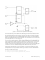
My Head Hurts, My Timing Stinks, and
I Don’t Love On-Chip Variation
Matt Weber
Silicon Logic Engineering, Inc
[email protected]
[email protected]
ABSTRACT
Abstract: Some ASIC vendors require designers to run static timing with on-chip variation
analysis. For the uninitiated, this task can be both confusing and frustrating. This paper will show
you:
1. Why on-chip variation analysis is important.
2. How to do on-chip variation analysis in Primetime.
3. How Primetime's on-chip variation analysis compares to Einstimer's linear combination of
delays (LCD).
4. Why some ASIC vendors require on-chip variation analysis and some don't.
Copyright © 2002 Silicon Logic Engineering, Inc. All Rights reserved.
No part of this publication may be reproduced, stored in a retrieval system, or transmitted in any form or by any
means without prior written permission from Silicon Logic Engineering, Inc.
In the U.S. and numerous other countries, SLE and the SLE logo are trademarks of Silicon Logic Engineering, Inc.
All other products or services mentioned herein may be trademarks of their respective owners.
About SLE
SLE is a semiconductor design services company that provides ASIC and system technology services to
the world's leading electronic systems and fabless semiconductor companies who require high-end chip
design expertise. SLE's ASICBlaster solution dramatically reduces the time it takes its customers to get
their products to market by offering a proven and repeatable design process, tools and semiconductor
intellectual property (SIP). Founded in 1996 by former Cray Research engineers, SLE is headquartered in
Eau Claire, Wisconsin.
Contact us: www.siliconlogic.com
Silicon Logic Engineering, Inc.
7 South Dewey Street
Eau Claire, Wisconsin 54701
800-757-9058
SNUGBoston 2002
2
[email protected]
1.0 Introduction
No two cells are the same. The same cell on two different chips could have dramatically different
timing characteristics. That is why static timing sign-off is never complete until runs have been
made with both the best-case and worst-case operating conditions. Additionally, two copies of
the same cell on the same chip can have different timing characteristics. This on-chip variation is
small compared to chip-to-chip variation. However, the effect still needs to be accounted for
somewhere in static timing analysis. One method is to use the on-chip variation analysis feature
of your static timing analysis tool.
2.0 What is on-chip variation?
Constructing a cell on an ASIC is a process that involves many variables. Some of these
variables are fairly consistent for the entire manufacturing process. Some variables vary from lot
to lot but are consistent across a single lot of wafers. Still other variables vary from wafer to
wafer but are consistent across a chip. Finally, some of the variations can occur within a single
chip.
Examples of variables that can occur on a single chip include small variations in the mask,
imperfections in optical proximity correction, and etch variations. Additionally, many of these
variations can occur over a very small area. Consider for example a string of buffers that are all
placed in a row. The gates in the middle of the string all have the same structures on each side,
but the gates at the ends of the string are adjacent to different features that may cause different
variations in the etching process.
The many variables involved in the manufacturing process mean the gate delay of a cell is really
a Gaussian distribution with a mean and standard deviation determined by the cell design and
these many variables. A randomly chosen instance of a cell on a randomly chosen chip could be
running at any point within that Gaussian distribution [figure 1]. Fortunately, timing analysis
does not need to directly verify the chip’s operation at every point in the distribution. Instead, if a
design is shown to work at both best case and worst case, it is assumed to work at any point in
between.
The cells on a single chip, however, still have their own distribution as in figure 1. Ignoring this
distribution by running only best case and worst case analysis can lead to problems which are
discussed in the next section.
SNUGBoston 2002
3
[email protected]
Gate Delay Distribution
0.018
0.14
0.016
0.12
0.014
0.1
0.012
0.01
0.08
0.008
0.06
Process
WC chip
0.006
0.04
0.004
0.02
0.002
0
200
225
250
275
300
325
0
350
Gate Delay (ps)
[Figure 1. Gaussian distributions for a manufacturing process and for a single, worst case chip.]
3.0 Problems that On-chip variation can cause
3.1 Setup Problems
The circuit in figure 3 shows one of the critical paths on the chip. While the differences in
loading of the clock drivers and parasitics of the clock nets will be included in calculating the
clock arrival times at the flops, the on-chip variation effects are not being considered when doing
a worst-case only analysis. If the clock path clock driver ends up being slightly faster than the
data path clock driver, there is a potential of manufacturing chips which have setup violations
that your static timing analysis didn’t tell you about.
Clk_3_1
Clk_1_1
Clk_2_1
Clk_1_2
[Figure 2. Critical path used in setup examples]
3.2 Hold Problems
In the circuit in figure 3, we have a very short logic path between two flops. Again, a worst-case
or best-case only analysis will consider loading and parasitics of the clock tree, but the on-chip
variation effects will not be modeled. If the data path clock driver ends up being slightly faster
than the clock path clock driver, there is a potential of manufacturing chips which have hold
violations that your static timing analysis didn’t tell you about.
SNUGBoston 2002
4
[email protected]
[Figure 3. Short path used in hold examples]
3.3 Clock Gating
The circuit in figure 4 is a clock gating circuit. It starts with a clock divider register. The clock
tree fanning out from there starts with a single clock buffer in the first level. The second level of
the clock tree has four clock drivers, one of which is a NAND gate performing a clock gating
function. To prevent glitches or pulse shrinkage caused by the clock gate, the gating input of the
NAND should only change when the clock input to the NAND is low. This is best accomplished
by using a negative edge triggered flip flop for the gating register. If the stage 1 clock driver and
the gating register are both modeled with worst case delays, but the clock to Q time of the gating
register ends up being a little bit faster, you have the potential for shortening the clock when you
enter power down mode and glitching the clock when you exit power down mode.
[Figure 4. Circuit used in clock gating examples]
SNUGBoston 2002
5
[email protected]
4.0 Timing without On-Chip variation
The appendices include the timing scripts that were used to constrain the chip for the examples
here. First let’s look at how the worst case path looks before we turn on on-chip variation
analysis. We have included the –path_type full_clock option to the report timing command so we
can watch what happens to the clock tree delays when OCV analysis gets turned on.
> report_timing -nosplit -input_pins -to [get_pins "$max_pin $clkgate_pin"] -path_type
full_clock
Startpoint: tx_ll/ct_arb/ct_man/mbst_rlt_1
(rising edge-triggered flip-flop clocked by clk_core)
Endpoint: tx_ll/ct_arb/ct_man/ct_ay_rg_43_4
(rising edge-triggered flip-flop clocked by clk_core)
Path Group: clk_core
Path Type: max
Point
Incr
Path
---------------------------------------------------------------------------clock clk_core (rise edge)
0.00
0.00
clock source latency
0.00
0.00
clk_core (in)
0.00
0.00 r
clk_core_box_3_1/A (CLK_Q)
0.00
0.00 r
clk_core_box_3_1/Z (CLK_Q)
0.17 +
0.17 r
clk_core_box_2_6/A (CLKI_O)
0.11 *
0.29 r
clk_core_box_2_6/Z (CLKI_O)
0.26 +
0.54 f
clk_core_box_1_69/A (CLKI_O)
0.07 *
0.62 f
clk_core_box_1_69/Z (CLKI_O)
0.18 +
0.80 r
tx_ll/ct_arb/ct_man/mbst_rlt_1/E (D_F_LPH0001_LPC_E)
0.01 *
0.81 r
tx_ll/ct_arb/ct_man/mbst_rlt_1/L2 (D_F_LPH0001_LPC_E)
0.41
1.22 f
tx_ll/ct_arb/ct_man/U1137/A (AND2_E)
0.01
1.23 f
…
……Data path removed from report
…
tx_ll/ct_arb/ct_man/U4921/Z (OA21_H)
0.14
4.17 f
tx_ll/ct_arb/ct_man/ct_ay_rg_43_4/D (D_F_LPH0002_LPC_E) 0.00
4.17 f
data arrival time
4.17
clock clk_core (rise edge)
3.76
3.76
clock source latency
0.00
3.76
clk_core (in)
0.00
3.76 r
clk_core_box_3_1/A (CLK_Q)
0.00
3.76 r
clk_core_box_3_1/Z (CLK_Q)
0.17 +
3.93 r
clk_core_box_2_6/A (CLKI_O)
0.11 *
4.05 r
clk_core_box_2_6/Z (CLKI_O)
0.26 +
4.30 f
clk_core_box_1_101/A (CLKI_O)
0.07 *
4.38 f
clk_core_box_1_101/Z (CLKI_O)
0.18 +
4.56 r
tx_ll/ct_arb/ct_man/ct_ay_rg_43_4/E (D_F_LPH0002_LPC_E) 0.01 *
4.57 r
clock uncertainty
-0.10
4.47
library setup time
-0.23
4.24
data required time
4.24
---------------------------------------------------------------------------data required time
4.24
data arrival time
-4.17
---------------------------------------------------------------------------slack (MET)
0.07
SNUGBoston 2002
6
[email protected]
The clock tree in this section of the chip happens to be perfectly balanced such that the clock
arrival time at the startpoint register is the same as the clock arrival time at the endpoint register.
The clock uncertainty is set to 100 ps to model PLL jitter. For the moment it looks like timing is
great, but we haven’t accounted for the possibility that, although clk_core_box_1_69 and
clk_core_box_1_101 are both modeled with worst case timing, in reality they may have slightly
different propagation delays. The clock nets that are not common to both paths may also
introduce some variability.
The tests on our short path and clock_gating hold check show similarly encouraging results.
> report_timing -nosplit -input_pins -delay min -to [get_pins "$min_pin
$clkgate_pin"] -path_type full_clock
Startpoint: tx_py/py_stat/o_tstat0
(rising edge-triggered flip-flop clocked by xi_tsclk)
Endpoint: tx_ll/basic/stat_ck/tstat_reg_0
(rising edge-triggered flip-flop clocked by xi_tsclk)
Path Group: xi_tsclk
Path Type: min
Point
Incr
Path
---------------------------------------------------------------------------clock xi_tsclk (rise edge)
0.00
0.00
clock source latency
0.00
0.00
xi_tsclk (in)
0.00
0.00 r
xi_tsclk_box_2_1/A (CLKI_Q)
0.00
0.00 r
xi_tsclk_box_2_1/Z (CLKI_Q)
0.24 +
0.24 f
xi_tsclk_box_1_10/A (CLKI_O)
0.16 *
0.40 f
xi_tsclk_box_1_10/Z (CLKI_O)
0.26 +
0.66 r
tx_py/py_stat/o_tstat0/E (D_F_LPH0001_H)
0.06 *
0.72 r
tx_py/py_stat/o_tstat0/L2 (D_F_LPH0001_H)
0.14
0.85 f
tx_ll/basic/stat_ck/U371/A (BUFFER_F)
0.00
0.85 f
tx_ll/basic/stat_ck/U371/Z (BUFFER_F)
0.09
0.94 f
tx_ll/basic/stat_ck/tstat_reg_0/D (D_F_LPH0001_LPC_E)
0.00
0.95 f
data arrival time
0.95
clock xi_tsclk (rise edge)
0.00
0.00
clock source latency
0.00
0.00
xi_tsclk (in)
0.00
0.00 r
xi_tsclk_box_2_1/A (CLKI_Q)
0.00
0.00 r
xi_tsclk_box_2_1/Z (CLKI_Q)
0.24 +
0.24 f
xi_tsclk_box_1_8/A (CLKI_O)
0.16 *
0.40 f
xi_tsclk_box_1_8/Z (CLKI_O)
0.26 +
0.66 r
tx_ll/basic/stat_ck/tstat_reg_0/E (D_F_LPH0001_LPC_E)
0.06 *
0.71 r
clock uncertainty
0.10
0.81
tx_ll/basic/stat_ck/tstat_reg_0/E (D_F_LPH0001_LPC_E)
0.81 r
library hold time
-0.03
0.78
data required time
0.78
---------------------------------------------------------------------------data required time
0.78
data arrival time
-0.95
---------------------------------------------------------------------------slack (MET)
0.17
SNUGBoston 2002
7
[email protected]
Startpoint: clk_rst_400/enable_clk_2nd_divby2_reg/E
(internal path startpoint clocked by clk_200)
Endpoint: clk_200_box_2_4
(rising clock gating-check end-point clocked by clk_200)
Path Group: **clock_gating_default**
Path Type: min
Point
Incr
Path
---------------------------------------------------------------------------clock clk_200 (fall edge)
2.50
2.50
clock source latency
0.72
3.22
clk_rst_400/clk_2nd_divby2_reg/L2 (D_LDR0001_E)
0.00
3.22 f
clk_rst_400/enable_clk_2nd_divby2_reg/E (D_LDF0001_E)
0.00
3.23 f
input external delay
0.00
3.23 f
clk_rst_400/enable_clk_2nd_divby2_reg/L2 (D_LDF0001_E) 0.41
3.63 r
clk_200_box_2_4/B (NAND2_O)
0.00
3.63 r
data arrival time
3.63
clock clk_200 (fall edge)
2.50
2.50
clock source latency
0.72
3.22
clk_rst_400/clk_2nd_divby2_reg/L2 (D_LDR0001_E)
0.00
3.22 f
clk_200_box_3_1/A (CLK_Q)
0.00
3.22 f
clk_200_box_3_1/Z (CLK_Q)
0.20 +
3.42 f
clk_200_box_2_4/A (NAND2_O)
0.06 *
3.49 f
clk_200_box_2_4/A (NAND2_O)
3.49 f
clock gating hold time
0.00
3.49
data required time
3.49
---------------------------------------------------------------------------data required time
3.49
data arrival time
-3.63
---------------------------------------------------------------------------slack (MET)
0.14
5.0 How to Model On-Chip Variation in Primetime
To do on-chip variation analysis, every timing arc in the design must have both a minimum and a
maximum delay which account for the on-chip variation. These are not the same delays that you
would use for a simple min-max analysis. Those delays represent the minimum and maximum
delays that will be seen across all chips from that process. For on-chip variation analysis, we
want the minimum and maximum delays that could be seen across a single chip. For on-chip
variation analysis we will make two analysis runs. The “slow-chip” analysis will set the
maximum delays at the worst case delays for the process and the minimum delays slightly faster
than that. For the “fast-chip” analysis, we will set the minimum delays to the best case delays for
the process, and we will set the maximum delays slightly slower than the best case delays.
Primetime has several methods for specifying these delays.
5.1 Annotate from one SDF file
If you are back-annotating delays from an SDF file, Primetime can get the delay values from the
min and max of the SDF triplet.
read_sdf –analysis_type on_chip_variation foo.sdf
SNUGBoston 2002
8
[email protected]
5.2 Annotate from two SDF files
Another choice is to read the data from two SDF files.
read_sdf –analysis_type on_chip_variation –min_file foo_min.sdf \
–max_file foo_max.sdf
5.4 Two Operating conditions
Sometimes you may have operating conditions specifically scaled for use with on-chip variation
analysis. For a slow chip analysis, the worst case operating condition is specified with –max and
the scaled worst case operating condition is specified with –min. For a fast chip analysis, the best
case operating condition is specified with –min and the scaled best case operating condition is
specified with –max.
set_operating_conditions –analysis_type on_chip_variation –min $WCOCV –max $WC
5.4 Single Operating condition
On-chip variation analysis can still be run even if you have only one operating condition. In this
case the minimum and maximum times are simply scaled versions of the delays determined from
the single operating condition that is loaded. The scaling factors are set by the set_timing_derate
command described next. This is the method that was used for this paper.
set_operating_conditions –analysis_type on_chip_variation $OP_CON
set_timing_derate –min 0.8 –max 1.0
5.5 Set_timing_derate
The set_timing_derate command can be used with any of the above methods to provide further
scaling of the timing paths. Scaling factors can be set independently for data paths, clock paths,
cell delays, net delays, and cell timing checks. If neither –clock nor -data is specified, the
derating factors apply to both clock and data paths. If –cell_delay, -net_delay, and –cell_check
are all omitted from the command, the derating factors apply to both cell and net delays, but not
to cell timing checks such as setup and hold times.
For example the following commands could be used to do a fast chip analysis with the best case
operating condition loaded, ten percent variation in cell delays, five percent variation in net
delays, and a five percent variation in cell timing checks.
set_operating_conditions –analysis_type on_chip_variation $BC_OP_CON
set_timing_derate –min 1.0 –max 1.10 –cell_delay
set_timing_derate –min 1.0 –max 1.05 –net_delay
set_timing_derate –min 1.0 –max 1.05 –cell_check
SNUGBoston 2002
9
[email protected]
6.0 My Timing Stinks!!
After two simple commands to turn on on-chip variation analysis, we find out that our timing
stinks and we don’t love on chip variation analysis.
set_operating_conditions -analysis_type on_chip_variation
set_timing_derate -min 0.8 -max 1.0
Here we are telling Primetime to assume that the min paths can be twenty percent faster than the
max paths. That’s a lot. More typically on-chip variation is modeled at six or eight or maybe ten
percent. Your ASIC or library vendor should tell you what is appropriate for the library that you
are using.
6.1 Setup Problems
When doing a setup test, the timing tool wants to verify that the latest possible data arrival can
still be captured by the earliest possible clock arrival at the endpoint register. The latest possible
data arrival is determined by taking the maximum delays along the clock path to the startpoint
register and the maximum delays along the slowest data path from the startpoint register to the
endpoint register. The earliest possible clock arrival at the endpoint register is determined by
taking the minimum delays along the clock path to the endpoint register.
Our long timing path, which previously had seventy picoseconds of positive slack, is now failing
by ninety picoseconds.
Startpoint: tx_ll/ct_arb/ct_man/mbst_rlt_1
(rising edge-triggered flip-flop clocked by clk_core)
Endpoint: tx_ll/ct_arb/ct_man/ct_ay_rg_43_4
(rising edge-triggered flip-flop clocked by clk_core)
Path Group: clk_core
Path Type: max
Min Clock Paths Derating Factor : 0.80
Point
Incr
Path
---------------------------------------------------------------------------clock clk_core (rise edge)
0.00
0.00
clock source latency
0.00
0.00
clk_core (in)
0.00
0.00 r
clk_core_box_3_1/A (CLK_Q)
0.00
0.00 r
clk_core_box_3_1/Z (CLK_Q)
0.17 +
0.17 r
clk_core_box_2_6/A (CLKI_O)
0.11 *
0.29 r
clk_core_box_2_6/Z (CLKI_O)
0.26 +
0.54 f
clk_core_box_1_69/A (CLKI_O)
0.07 *
0.62 f
clk_core_box_1_69/Z (CLKI_O)
0.18 +
0.80 r
tx_ll/ct_arb/ct_man/mbst_rlt_1/E (D_F_LPH0001_LPC_E)
0.01 *
0.81 r
tx_ll/ct_arb/ct_man/mbst_rlt_1/L2 (D_F_LPH0001_LPC_E)
0.41
1.22 f
tx_ll/ct_arb/ct_man/U1137/A (AND2_E)
0.01
1.23 f
…
……Data path removed from report
…
tx_ll/ct_arb/ct_man/U4921/Z (OA21_H)
0.14
4.17 f
tx_ll/ct_arb/ct_man/ct_ay_rg_43_4/D (D_F_LPH0002_LPC_E) 0.00
4.17 f
data arrival time
4.17
SNUGBoston 2002
10
[email protected]
clock clk_core (rise edge)
3.76
3.76
clock source latency
0.00
3.76
clk_core (in)
0.00
3.76 r
clk_core_box_3_1/A (CLK_Q)
0.00
3.76 r
clk_core_box_3_1/Z (CLK_Q)
0.14 +
3.90 r
clk_core_box_2_6/A (CLKI_O)
0.09 *
3.99 r
clk_core_box_2_6/Z (CLKI_O)
0.21 +
4.20 f
clk_core_box_1_101/A (CLKI_O)
0.06 *
4.25 f
clk_core_box_1_101/Z (CLKI_O)
0.14 +
4.40 r
tx_ll/ct_arb/ct_man/ct_ay_rg_43_4/E (D_F_LPH0002_LPC_E) 0.01 *
4.41 r
clock uncertainty
-0.10
4.31
library setup time
-0.23
4.08
data required time
4.08
---------------------------------------------------------------------------data required time
4.08
data arrival time
-4.17
---------------------------------------------------------------------------slack (VIOLATED)
-0.09
The path that is timed with maximum delays, the data path, shows the same timing as before.
However, the clock latency to the endpoint register, using minimum delays, is now 160 ps faster
than before.
6.2 Hold Problems
When doing a hold test, the timing tool wants to verify that the earliest possible data arrival does
not arrive at the endpoint register before the latest possible clock arrival. So we use min delays
for the clock path to the startpoint register, min delays through the shortest data path, and max
delays for the clock path to the endpoint register.
Here again, a previously passing timing check has now started to fail.
Startpoint: tx_py/py_stat/o_tstat0
(rising edge-triggered flip-flop clocked by xi_tsclk)
Endpoint: tx_ll/basic/stat_ck/tstat_reg_0
(rising edge-triggered flip-flop clocked by xi_tsclk)
Path Group: xi_tsclk
Path Type: min
Min Data Paths Derating Factor : 0.80
Min Clock Paths Derating Factor : 0.80
Point
Incr
Path
---------------------------------------------------------------------------clock xi_tsclk (rise edge)
0.00
0.00
clock source latency
0.00
0.00
xi_tsclk (in)
0.00
0.00 r
xi_tsclk_box_2_1/A (CLKI_Q)
0.00
0.00 r
xi_tsclk_box_2_1/Z (CLKI_Q)
0.19 +
0.19 f
xi_tsclk_box_1_10/A (CLKI_O)
0.13 *
0.32 f
xi_tsclk_box_1_10/Z (CLKI_O)
0.21 +
0.53 r
tx_py/py_stat/o_tstat0/E (D_F_LPH0001_H)
0.04 *
0.57 r
tx_py/py_stat/o_tstat0/L2 (D_F_LPH0001_H)
0.11
0.68 f
tx_ll/basic/stat_ck/U371/A (BUFFER_F)
0.00
0.68 f
tx_ll/basic/stat_ck/U371/Z (BUFFER_F)
0.07
0.76 f
tx_ll/basic/stat_ck/tstat_reg_0/D (D_F_LPH0001_LPC_E)
0.00
0.76 f
data arrival time
0.76
SNUGBoston 2002
11
[email protected]
clock xi_tsclk (rise edge)
0.00
0.00
clock source latency
0.00
0.00
xi_tsclk (in)
0.00
0.00 r
xi_tsclk_box_2_1/A (CLKI_Q)
0.00
0.00 r
xi_tsclk_box_2_1/Z (CLKI_Q)
0.24 +
0.24 f
xi_tsclk_box_1_8/A (CLKI_O)
0.16 *
0.40 f
xi_tsclk_box_1_8/Z (CLKI_O)
0.26 +
0.66 r
tx_ll/basic/stat_ck/tstat_reg_0/E (D_F_LPH0001_LPC_E)
0.06 *
0.71 r
clock uncertainty
0.10
0.81
tx_ll/basic/stat_ck/tstat_reg_0/E (D_F_LPH0001_LPC_E)
0.81 r
library hold time
-0.03
0.78
data required time
0.78
---------------------------------------------------------------------------data required time
0.78
data arrival time
-0.76
---------------------------------------------------------------------------slack (VIOLATED)
-0.02
As expected, the clock pin at the endpoint register has the same arrival time as it did before, but
the data path is now 190ps faster.
6.3 Clock Gating Problems
With an AND gate, we want to verify that the gating signal can only change while the clock is
low. A hold check is done to verify that the gating signal changes after the falling edge of the
clock, and a setup check is done to verify that the gating signal changes before the next rising
edge of the clock. We’re not looking at the setup check here because it has lots of positive slack
and is therefore not very interesting. The hold check is going to use min delays along the gating
path and max delays along the clock path.
Startpoint: clk_rst_400/enable_clk_2nd_divby2_reg/E
(internal path startpoint clocked by clk_200)
Endpoint: clk_200_box_2_4
(rising clock gating-check end-point clocked by clk_200)
Path Group: **clock_gating_default**
Path Type: min
Min Data Paths Derating Factor : 0.80
Min Clock Paths Derating Factor : 0.80
Point
Incr
Path
---------------------------------------------------------------------------clock clk_200 (fall edge)
2.50
2.50
clock source latency
0.58
3.08
clk_rst_400/clk_2nd_divby2_reg/L2 (D_LDR0001_E)
0.00
3.08 f
clk_rst_400/enable_clk_2nd_divby2_reg/E (D_LDF0001_E)
0.00
3.08 f
input external delay
0.00
3.08 f
clk_rst_400/enable_clk_2nd_divby2_reg/L2 (D_LDF0001_E) 0.33
3.41 r
clk_200_box_2_4/B (NAND2_O)
0.00
3.41 r
data arrival time
3.41
clock clk_200 (fall edge)
clock source latency
clk_rst_400/clk_2nd_divby2_reg/L2 (D_LDR0001_E)
clk_200_box_3_1/A (CLK_Q)
clk_200_box_3_1/Z (CLK_Q)
clk_200_box_2_4/A (NAND2_O)
clk_200_box_2_4/A (NAND2_O)
clock gating hold time
SNUGBoston 2002
12
2.50
0.72
0.00
0.00
0.20 +
0.06 *
0.00
2.50
3.22
3.22
3.22
3.42
3.49
3.49
3.49
f
f
f
f
f
[email protected]
data required time
3.49
---------------------------------------------------------------------------data required time
3.49
data arrival time
-3.41
---------------------------------------------------------------------------slack (VIOLATED)
-0.08
7.0 What is Clock Reconvergence Pessimism Removal?
Taking a careful look at the timing reports above, we can see that we are being unfairly punished.
For example, in the setup case, clock driver clk_core_box_3_1 is in both the data path and the
clock path. In the data path it is given a propagation time of 170ps, while in the clock path it is
given a propagation time of 140ps. While the propagation delay of that cell could be either 140ps
or 170ps, it can’t be both! If the propagation delay for an edge on its way to the data path was
170ps, then it was also 170ps on its way to the clock path. To assume differently is overly
pessimistic.
Primetime is able to correct this problem through an algorithm called clock reconvergence
pessimism removal (CRPR). To enable CRPR, simply set the appropriate variable.
set timing_remove_clock_reconvergence_pessimism true
Lets’see what it does to our failing setup test:
Startpoint: tx_ll/ct_arb/ct_man/mbst_rlt_1
(rising edge-triggered flip-flop clocked by clk_core)
Endpoint: tx_ll/ct_arb/ct_man/ct_ay_rg_43_4
(rising edge-triggered flip-flop clocked by clk_core)
Path Group: clk_core
Path Type: max
Min Clock Paths Derating Factor : 0.80
Point
Incr
Path
---------------------------------------------------------------------------clock clk_core (rise edge)
0.00
0.00
clock source latency
0.00
0.00
clk_core (in)
0.00
0.00 r
clk_core_box_3_1/A (CLK_Q)
0.00
0.00 r
clk_core_box_3_1/Z (CLK_Q)
0.17 +
0.17 r
clk_core_box_2_6/A (CLKI_O)
0.11 *
0.29 r
clk_core_box_2_6/Z (CLKI_O)
0.26 +
0.54 f
clk_core_box_1_69/A (CLKI_O)
0.07 *
0.62 f
clk_core_box_1_69/Z (CLKI_O)
0.18 +
0.80 r
tx_ll/ct_arb/ct_man/mbst_rlt_1/E (D_F_LPH0001_LPC_E)
0.01 *
0.81 r
tx_ll/ct_arb/ct_man/mbst_rlt_1/L2 (D_F_LPH0001_LPC_E)
0.41
1.22 f
tx_ll/ct_arb/ct_man/U1137/A (AND2_E)
0.01
1.23 f
…
……Data path removed from report
…
tx_ll/ct_arb/ct_man/U4921/Z (OA21_H)
0.14
tx_ll/ct_arb/ct_man/ct_ay_rg_43_4/D (D_F_LPH0002_LPC_E) 0.00
data arrival time
clock clk_core (rise edge)
clock source latency
SNUGBoston 2002
3.76
0.00
13
4.17 f
4.17 f
4.17
3.76
3.76
[email protected]
clk_core (in)
0.00
3.76 r
clk_core_box_3_1/A (CLK_Q)
0.00
3.76 r
clk_core_box_3_1/Z (CLK_Q)
0.14 +
3.90 r
clk_core_box_2_6/A (CLKI_O)
0.09 *
3.99 r
clk_core_box_2_6/Z (CLKI_O)
0.21 +
4.20 f
clk_core_box_1_101/A (CLKI_O)
0.06 *
4.25 f
clk_core_box_1_101/Z (CLKI_O)
0.14 +
4.40 r
tx_ll/ct_arb/ct_man/ct_ay_rg_43_4/E (D_F_LPH0002_LPC_E) 0.01 *
4.41 r
clock reconvergence pessimism
0.11
4.52
clock uncertainty
-0.10
4.42
library setup time
-0.23
4.19
data required time
4.19
---------------------------------------------------------------------------data required time
4.19
data arrival time
-4.17
---------------------------------------------------------------------------slack (MET)
0.01
The timing report is identical to what we had before CRPR was turned on, with one important
exception. Primetime has looked at the cells and nets which are common between the data path
and the clock path, calculated the difference between their min and max times, and used the total
as an adjust to the clock path. This adjustment shows up in a new line called “clock
reconvergence pessimism.”
With this adjustment, our setup check is now passing! The hold and clock gating tests pass now
also with +30ps and +60ps of slack respectively.
Because it noticeably increases runtime and memory usage, the CRPR algorithm is turned off by
default. One option for reducing the impact on runtime and memory usage is to allow some
amount of clock reconvergence pessimism to remain in the analysis. The variable
timing_crpr_threshold_ps specifies the pessimism removal threshold. Its default value is
20ps which allows 20ps of reconvergence pessimism to remain in the analysis.
8.0 How Primetime’s On-Chip Variation Analysis compares to Einstimer’s
linear combination of delays (LCD)
Users of IBM’s Einstimer static timing analysis tool have been doing on-chip variation analysis
for years. In Einstimer the process is called “linear combination of delays” or LCD mode. The
concepts are the same. Every point has both a min (called early) and a max (called late) time. A
setup check tests the late data arrival time against the early clock arrival time. A hold check tests
the early data against the late clock. However, Einstimer is different in the way that those early
and late arrival times are calculated.
In Primetime, when you specify an operating condition, you are specifying the temperature,
voltage, and process point that the cells are going to be modeled at. In Einstimer, you set the
temperature and voltage for the analysis that you want to do, but you don’t specify a process
point. Einstimer is going to use both the best and worst process points in its calculations. Every
path in the design has both a best case delay and a worst case delay for the specified temperature
and voltage. However, these delays represent the variation of the entire manufacturing process,
SNUGBoston 2002
14
[email protected]
not the variation found on a single chip. You then tell Einstimer what timing mode you would
like to run in. Best case mode is typically run with high voltage and low temperature. Worst case
mode is typically run with low voltage and high temperature. LCD mode is what we really want
to do, and it is typically run twice. First it is run with low voltage and high temperature to do our
slow chip analysis. Then it is re-run with high voltage and low temperature to do our fast chip
analysis.
Because the best case delay and worst case delay that are associated with the paths in the design
represent the entire process instead of a single chip, they are not directly used against each other.
Instead, they are combined to come up with the early and late times that are used for the setup,
hold, and other timing checks. The differences between best, worst, early, and late arrival times
are a frequent source of confusion, so it is worth repeating.
Ø Best/Worst : Represent variation of entire process, not timed against each other, defined at a
specific voltage and temperature.
Ø Early/Late : Represent the variation of on a single chip, are timed against each other,
calculated from the best case and worst case values.
The early and late arrival times are calculated from the best case and worst case numbers using a
set of scaling factors. For a slow chip analysis the factors may look like this:
Early
Late
Best
0.10
0.00
Nom
0.00
0.00
Worst
0.90
1.00
These factors tell Einstimer that the early arrival times are calculated by adding together the best
case time multiplied by 0.10 and the worst case time multiplied by 0.90. The late arrival times
are simply the worst case times. In practice the factor that is multiplied against the nominal case
number is always zero.
Factors for a fast chip analysis may look like this:
Early
Late
Best
1.00
0.90
Nom
0.00
0.00
Worst
0.00
0.10
As you would expect, Einstimer has a capability similar to Primetime’s CRPR. The name of the
function and its abbreviation are also similar. In Einstimer it is called “common path pessimism
removal” or CPPR.
9.0My head hurts, my FETs stink
The SPI-4 IP core that we’ve been using for these examples includes a source synchronous DDR
output that serves to illustrate another consideration when running on-chip variation. Paul
Zimmer and Andrew Cheng presented a paper [1] at San Jose SNUG this year detailing how to
set up timing for this type of an interface. The basic circuit looks like this:
SNUGBoston 2002
15
[email protected]
[Figure 5. Circuit for source synchronous DDR output]
This circuit looks like a perfect candidate for CRPR. Except for the final mux and the IO driver,
the clock and data paths are entirely common. Our check for the duty cycle on the clock output
should be even better. Obviously, a rising edge going from the reference clock input to clkout is
going to go through all the same cells as a falling edge. We would expect to receive CRPR credit
for the entire path. The OCV effect will be zero.
However, this is somewhat optimistic. While a rising and falling edge will run through all of the
same cells and nets, the timing is controlled by different FETs within each cell. The PFETs and
NFETs within a cell are not necessarily identical. In essence, there can be some “cross-cell
variation.” Just because a rising edge through a cell is at worst case, does not mean a falling edge
will also be at worst case. Therefore allowing the full CRPR credit is really not accurate.
Primetime does not model these “cross-cell variations” at all. Even if it wanted to, the proper
information does not exist in the libraries for this type of analysis to be done. What Primetime
does offer is a simple on/off switch.
set timing_clock_reconvergence_pessimism normal
set timing_clock_reconvergence_pessimism same_transition
SNUGBoston 2002
16
[email protected]
When the timing_clock_reconvergence_pessimism variable is set to normal (the default
setting), Primetime conveniently ignores the potential differences between FETs within a cell,
and you are given the entire CRPR credit. When the variable is set to same_transition, Primetime
assumes there is no correlation between the FETs, and you get zero CRPR credit in cases where
opposite edges through a cell are being timed against each other. This assumption is overly
pessimistic and can cause many false failures on tests that include opposite edges. Examples are:
1. Paths between negedge and posedge registers.
2. Duty cycle checks.
3. Clock gating checks and other circuits in clock generation logic.
The static timing engineer must choose (with the library vendor’s guidance) between being
optimistic, being pessimistic, or writing a bunch of Tcl to manually do the appropriate tests.
Einstimer, by the way, always gives you zero credit for opposite edge transitions. (In other words,
there is no way to be optimistic when running Einstimer.)
10.0
How OCV Analysis improves silicon performance
Although at first it appears that using on-chip variation analysis steals a bunch of performance
from you, I don't think this is necessarily the case. While many ASIC vendors do not require you
to run OCV analysis, this does not mean that they have figured out how to build chips with zero
variation. If the vendor does not have a manufacturing test that can catch the failures, or if they
are not willing to accept the resulting yield loss, they must still account for on-chip variations
during static timing analysis. It may be done through padding the setup and hold margins of the
flops, requiring extra set_clock_uncertainty even after the clocks are placed and routed, or
requiring XXps of positive slack for timing signoff. Any of these methods effectively penalize
ALL of the paths in your design. In the setup example above, if the vendor wanted us to increase
the clock uncertainy to 200ps instead of running OCV we would still have a failing path. Instead
of a tape-out on Friday, we would be working the weekend.
By running on-chip variation analysis, and more specifically the CRPR algorithm, we are able to
stuff an extra hundred picoseconds of logic into paths that are contained in a common branch of
the clock tree. By modeling the on-chip variation effect more accurately, we are able to get more
performance out of the design.
SNUGBoston 2002
17
[email protected]
11.0
Conclusions and Recommendations
Most static timing analysis done today does not include on-chip variation analysis. In fact, I
know of only two ASIC vendors who require this type of analysis. However, as clock frequencies
continue to increase and process geometries continue to decrease, I believe on-chip variation
analysis will become more common.
This paper has shown how OCV analysis is run, what the reports look like in Primetime, and
how OCV analysis has the potential to increase the performance that we get from our silicon.
For those who will be running OCV analysis on their next static timing project, I have four
suggestions:
1. Keep this paper close at hand.
2. Turn on on-chip variation mode as soon as you have a real clock tree in the design,
perhaps even before. The last week before tape-out is NOT the time to find out that you
have several hundred failing paths.
3. Don’t forget to turn on CRPR.
4. Send me an e-mail if you need any help.
With these suggestions, I hope you can avoid “Wasting away again in static-timing-ville.”
12.0
References
[1] A. Cheng and P. Zimmer, “Working with DDRs in PrimeTime”, SNUG San Jose 2002
[] There is also a lot of good information in the PrimeTime user’s manual
SNUGBoston 2002
18
[email protected]
13.0
Appendix A – Tcl code for timing constraints
# Load library
set search_path ". /techlibs/$LIBRARY/$VERSION/synthesis/synopsys ./sv"
set SYN_LIB {$LIBRARY}
set link_path "* $LIBRARY.db"
# Load design
read_verilog sle_spi4_tx_block.v
link_design sle_spi4_tx_block
current_design sle_spi4_tx_block
# Set environment
set_wire_load_model -library $LIBRARY -name $WIRELOAD_MODEL
set_wire_load_mode top
set auto_wire_load_selection {false}
set_operating_conditions -analysis_type bc_wc
# Get parasitics
source sle_spi4_tx_block.cap.tcl
source sle_spi4_tx_block.rc.tcl
# Create Clocks
set core_freq 266
create_clock -period [expr 1000.0 / $core_freq] -name clk_core [get_ports clk_core]
set_clock_uncertainty 0.10 clk_core
set_propagated_clock clk_core
create_clock -period 10.0 -name xi_tsclk [get_ports xi_tsclk]
set_clock_uncertainty 0.10 xi_tsclk
set_propagated_clock xi_tsclk
create_clock -period 2.5 -name xi_xtalclk [get_ports xi_xtalclk]
set_clock_uncertainty 0.10 xi_xtalclk
set_propagated_clock xi_xtalclk
create_generated_clock -name clk_200 -source [get_ports xi_xtalclk] -divide_by 2 [get_pins
clk_rst_400/clk_2nd_divby2_reg/L2]
set_propagated_clock clk_200
# clk_core is asynch to the other clocks
set_false_path -from clk_core -to [remove_from_collection [all_clocks] [get_clocks "clk_core"]]
set_false_path -from [remove_from_collection [all_clocks] [get_clocks "clk_core"]] -to clk_core
# Inputs and Outputs are mostly clk_core
set_input_delay 1.0 -clock clk_core [remove_from_collection [all_inputs] [get_ports "clk_core
xi_tsclk xi_xtalclk"]]
set_output_delay [expr 1000.0 / $core_freq – 1.0] -clock clk_core [remove_from_collection
[all_outputs] [get_ports "xo_tdclk xo_tdat* xo_tctl"]]
group_path -name outputs -to [remove_from_collection [all_outputs] [get_ports "xo_tdclk xo_tdat*
xo_tctl"]]
# These are the exceptions
set_input_delay 1.0 -clock xi_tsclk [get_ports xi_tstat*]
# By default, outputs are clk_core. This bus, however is source synchronous DDR
# We will time it with two virtual clocks as described by Paul Zimmer and Andrew Cheng's
# SNUG San Jose 2002 paper
source setup_ddr_out_timing.tcl
_setup_ddr_out_timing [list xo_tdat* xo_tctl] xo_tdclk xi_xtalclk 0.280 0.280
# Ready to generate reports
SNUGBoston 2002
19
[email protected]
14.0 Appendix B – Tcl code for DDR output timing constraints
##################################################################
#
# Copyright 2002 by Silicon Logic Engineering. All rights reserved
#
##################################################################
#
# File name
: setup_ddr_out_timing.tcl
# Author
: Matt Weber
# Revision
: $Id$
#
##################################################################
#
# Description : This Tcl procedure sets up DDR output timing
#
constraints similar to the virtual clock approach
#
suggested in Paul Zimmer and Andrew Cheng's
#
SNUG San Jose 2002 paper
#
The inputs are as follows:
#
_data_output : The name of the data output pin or bus
#
_clk_output : The name of the clock output pin
#
_source_input : The name of the reference clock
#
which creates the clock and data outputs
#
_maxskew0 : Maximum time that data_output can change
#
before transition on clk_output
#
_maxskew1 : Maximum time that data_output can change
#
after transition on clk_output
#
An assumption is made that the data output is
#
created by a mux with pin names D0, D1, and SD
#
IMPORTANT : The script is not complete yet. To fully
#
time these outputs several things need to checked:
#
1. Skew between clock and data outputs
#
2. Duty cycle of clock output
#
3. Jitter of data outputs. Since this is DDR, duty
#
cycle on the data outputs looks like jitter.
#
At this time only the first check is being done.
#
##################################################################
proc _setup_ddr_out_timing {_data_output _clk_output _source_input _maxskew0 _maxskew1} {
# Get all the attibutes from the source clock so we can make good copies
set _source_period [get_attribute [get_clocks $_source_input] period]
set _source_waveform_junk [split [get_attribute [get_clocks $_source_input] waveform] " {}"]
set _source_waveform "[lindex $_source_waveform_junk 1] [lindex $_source_waveform_junk 2]"
set _source_setup_uncertainty [get_attribute [get_clocks $_source_input] setup_uncertainty]
set _source_hold_uncertainty [get_attribute [get_clocks $_source_input] hold_uncertainty]
# Then get the rising edge latency from source_input to clk_output
set _path [get_timing_paths -from [get_ports $_source_input] -to [get_ports $_clk_output] delay max_rise]
set _rise_latency [get_attribute $_path arrival]
# Then the falling edge latency from source_input to clk_output
set _path [get_timing_paths -from [get_ports $_source_input] -to [get_ports $_clk_output] delay max_fall]
set _fall_latency [get_attribute $_path arrival]
# Create a virtual clock to use for comparisions to rising edge of clk_output
set posclkname [format %s_posclkout $_clk_output]
create_clock -period $_source_period -waveform $_source_waveform -name $posclkname
set_clock_latency $_rise_latency -rise -source [get_clocks $posclkname]
set_clock_latency $_fall_latency -fall -source [get_clocks $posclkname]
set_clock_uncertainty -setup $_source_setup_uncertainty $posclkname
set_clock_uncertainty -hold $_source_hold_uncertainty $posclkname
# Create another virtual clock to use for comparisions to falling edge of clk_output
set negclkname [format %s_negclkout $_clk_output]
create_clock -period $_source_period -waveform $_source_waveform -name $negclkname
set_clock_latency $_rise_latency -rise -source [get_clocks $negclkname]
set_clock_latency $_fall_latency -fall -source [get_clocks $negclkname]
set_clock_uncertainty -setup $_source_setup_uncertainty $negclkname
set_clock_uncertainty -hold $_source_hold_uncertainty $negclkname
# Set output delays for data_output.
# _maxskew0, the maximum amount of time that the data output can change before the clock output
#
is really a hold test
set_output_delay $_maxskew0 -clock $posclkname [get_ports $_data_output] -min
set_output_delay $_maxskew0 -clock $negclkname [get_ports $_data_output] -min -add_delay clock_fall
SNUGBoston 2002
20
[email protected]
# _maxskew1, the maximum amount of time that the data output can change after the clock output
#
is really a setup test
set_output_delay [expr $_source_period/2.0 - $_maxskew1] -clock $posclkname [get_ports
$_data_output] -max -add_delay
set_output_delay [expr $_source_period/2.0 - $_maxskew1] -clock $negclkname [get_ports
$_data_output] -max -add_delay -clock_fall
# For DDR outputs built with posedge/negedge regs followed by a mux, assume data from
#
the D0 side of the mux gets captured by posclkout virtual clock, and data from the
#
D1 side gets captured by the negclkout virtual clock
# The loops here seem to be pretty slow. Should look for a better way. Or hardcode the
#
relavant gate names so we don’t have to do this search for them.
foreach_in_collection temp_output [get_ports $_data_output] {
foreach_in_collection temp_path [get_timing_paths -to [get_ports $temp_output] -delay
max_rise] {
foreach_in_collection temp_point [get_attribute $temp_path points] {
set object [get_attribute $temp_point object]
set point_name [get_attribute $object full_name]
if {[string match */D0 $point_name] } {
echo "_setup_ddr_out_timing is setting false_path from $point_name to virtual clock
$negclkname for setup checks"
set_false_path -setup -through [get_pins $point_name] -to [get_clocks $negclkname]
}
if {[string match */D1 $point_name] } {
echo "_setup_ddr_out_timing is setting false_path from $point_name to virtual clock
$posclkname for setup checks"
set_false_path -setup -through [get_pins $point_name] -to [get_clocks $posclkname]
}
}
}
}
}
SNUGBoston 2002
21
[email protected]