1
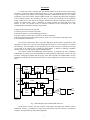
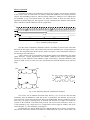
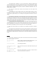
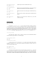
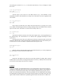
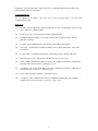
EUROPEAN ORGANIZATION FOR NUCLEAR RESEARCH
ORGANISATION EUROPEENNE POUR LA RECHERCHE NUCLEAIRE
CERN - PS DIVISION
PS/BD Note 96-02(Tech)
The VMOD-TRX: A device for communicating with remote instrumentation
A. Barreira Sevillano, J.M. Belleman
Abstract
This module has been developed to exchange data between the VME-based control system and
instrumentation in the PS accelerator and transfer line tunnels. We needed a simple data
communications device, but a survey of commercially available devices showed a lack of suitable
products. The VMOD-TRX is a piggy-back for use with the JANZ VMOD-IO VME module, and
provides bi-directional high-speed serial data communication over up to 300m of twisted pair cable.
Simple software routines to interface to user applications are described.
Geneva, Switzerland
May 20, 1996
Introduction
To satisfy the need to exchange data with instrumentation in the PS accelerator and transfer
line tunnels, we needed a simple communication device. A survey of available circuits brought to light
a large void between the simple and very high performance communication links like, e.g., AMD’s
TAXIchip [1], the slow but fairly complex UARTs and the very complex networking chips commonly
used in computer systems. The TAXIchip is too fast to be used over twisted pairs of any significant
length. UARTs are too slow and need a computer at both ends of the link. Networking chips are more
complex still than UARTs. There is apparently no simple moderate-speed data link chip on the
market. To meet our peculiar needs, we therefore embarked on the development of a data
communications link with the following requirements:
• Simple bi-directional point to point link.
• No micro-processors in remote equipment.
• Galvanic isolation to avoid introducing ground loops.
• No opto-couplers, because they are known to fail under irradiation.
• Bit serial communication at the highest practical speed over at least 300m of twisted pair cable.
• Good immunity to interference.
The result was dubbed the TRX. It provides high-speed point-to-point communication with
equipment in remote areas. The core of the design takes the form of a list of equations to be burned
into a PLD [2]. The TRX employs a serial protocol over two twisted wire pairs, sending and receiving
16 bit words at an effective rate of slightly less than 1Mbit/s. A number of mutually compatible
variants exists to cope with specific types of instrumentation.
One of these variants, the VMOD-TRX, described below, is designed to fit onto a VMOD-IO
VME module [3]. Both receiver and transmitter are buffered with 256-word FIFOs to relieve the host
processor of keeping up with the data rate proper of the TRX. Presently, the VMOD-TRX is used to
communicate with the TT2 and TT70 transfer line PUs. The CODD PUs are also foreseen to be using
them.
D00-D15
16
FIFO
256x16
16
16
MR FE FF
Serial data out
MDT
TXB TXRQ
LB
Control
EN,MA0
MDT
RS485
driver
Manchester
TS TXB TXRQ
MR FE FF R
D00-D15
NRZ
TX
MR FE FF
RXB
LOOPBACK
E CARRIER
IRQ
CARRIER
DETECT
MR FE FF W
D00-D15
16
FIFO
256x16
RS RXB
16
E
CK
CK
RX
D
NRZ
MDR
RS485
receiver
Manchester
Serial data in
MDR
VMOD-IO
MODULBUS
CONNECTOR
Fig. 1: Block diagram of the VMOD-TRX transceiver
Nearly all the circuitry, with the exception of the FIFOs, the RS485 line interface and the
Manchester decoder, is contained in a single Altera 7064 EPLD. The line interface is transformer
coupled to avoid ground loops with remote equipment.
1
Theory of operation
The transceiver employs an isochronous serial protocol [4]. Data is sent in frames, consisting
of one or more words. A word consists of a start bit, 16 data bits (MSB first), an even parity bit and a
stop bit. The transmitting sequence is started by taking /TXRQ low. /TXB goes low to indicate that
the transmitter is busy. The transmit strobe, /TS, marks the instants at which new data must be
applied at the parallel input port. This sequence of events is matched to the operation of the transmit
FIFO, such that its current contents are sent as a single frame.
CK
STATE
idle
start
D15
D14
D13
D4
D3
D2
D1
D0
parity
stop
start
D15
D14
D13
D4
D3
D2
D1
D0
parity
stop
idle
idle
idle
TXRQ
TS
TXB
Word 1
Word 2
Frame
Fig. 2: Transmitter timing diagram
The data stream is Manchester modulated, which is essentially an exclusive-OR of the NRZ
data with the shift register clock. This combines data and clock information into a single signal and
removes DC components from the data stream, which is necessary to allow transformer coupling of
the twisted pair wire interconnect.
A mere exclusive-OR of clock and data would produce glitches in the Manchester code output
signal. Therefore, a simple asynchronous state machine (ASM) has been used to implement this
function [5,6]. This ASM takes clock and data as input, and produces a glitch-free Manchester data
stream as output. It does so at the cost of one extra macrocell in the PLD and half a clock period of
delay.
Ck D
M=0
00
Ck
M=1
01
Ck
Ck D
Ck D
D
M
Ck D
10
M=0
Ck
11
M=1
Fig. 3: State and timing diagrams of Manchester modulator
The receiver uses an MAD85 from Data Delay Devices [7] to recover the clock and data
information from the Manchester coded data stream. A synchronous state machine, driven by the
recovered clock, converts the serial data back into 16 bit parallel format. Data are put into the receiver
FIFO only if no parity or framing errors are detected. The detection of a single error entails the
rejection of the remainder of the frame being received. The receiver treats consecutive words, i.e.,
words separated by only a single stop bit, as a single frame, and will signal its readiness only at the
end of the frame, i.e., after detecting a second stop bit.
Upon detection of a start bit, /RXB goes low to indicate that the receiver is busy. It remains low
until the end of the frame. Parallel received data is available during the stop and continue states, and
2
the rising edge of /RS can be used to latch it. /RS remains high if an error was detected in the current
frame.
CK
Serial data in
STATE
start
idle
D15
D15
D14
D14
D13
D13
D4
D4
D3
D3
D2
D2
D1
D1
D0
D0
parity
parity
stop
start
stop continue D15
D15
D14
D14
D13
D13
D4
D4
D3
D3
D2
D2
D1
D1
D0
D0
parity
parity
stop
stop continue idle
idle
idle
data
RS
RXB
Word 1
Word 2
Frame
Fig. 4: Receiver timing diagram
When at first a connection between a transmitter and a receiver is made, and in the absence of
any data transitions, the Manchester demodulator has no way of knowing the correct phase of the
clock signal. As Murphy’s law predicts, it generally selects the wrong initial phase. When the first
word is transferred, it drops into the right phase. This is too late to actually correctly transfer that first
word. This implies that a training sequence, consisting of at least one arbitrary word, must be
transmitted to force the demodulator into the correct phase. This is also the case when the loopback
mode is being switched on or off.
Wiring
The serial line connections are brought out on the P2 connector at the rear of the VME crate
[8]. Connections between transmitters and receivers are to be made using preferably screened twisted
pair wire of approximately 100Ω impedance. The maximum wire length over which reliable
communication can be expected is about 300m, depending on the cable quality and the induced noise
levels. The pin numbers used are detailed in the table below. MODULbus is the term employed by
JANZ Computer AG to denote the bus interconnecting the piggy-back modules on a VMOD-IO card.
P2 pin
1a
1c
2a
2c
9a
9c
10a
10c
17a
17c
18a
18c
25a
25c
26a
26c
Transmitted data (true)
Transmitted data (complement)
Received data (true)
Received data (complement)
Transmitted data (true)
Transmitted data (complement)
Received data (true)
Received data (complement)
Transmitted data (true)
Transmitted data (complement)
Received data (true)
Received data (complement)
Transmitted data (true)
Transmitted data (complement)
Received data (true)
Received data (complement)
MDT0
/MDT0
MDR0
/MDR0
MDT1
/MDT1
MDR1
/MDR1
MDT2
/MDT2
MDR2
/MDR2
MDT3
/MDT3
MDR3
/MDR3
MODULbus
Socket 0
MODULbus
Socket 1
MODULbus
Socket 2
MODULbus
Socket 3
Table A: Twisted pair wiring pin allocations on VME J2
3
Addressing
Each transceiver appears in the memory space of the VMOD-IO module as two consecutive 16
bit words, the first being the data, and the second the control register. Data written into the first
address is put into the transmit FIFO prior to being sent, and data received and stored in the receive
FIFO can be read from it. The control register informs about and controls the state of the FIFOs and
of the transmitter and receiver sections of the device. In accordance with PS/CO preferences, the base
address of the first VMOD-IO in a crate is set to 0xffff6000. Further modules, if any, are situated at
0x800 intervals above that. [9]
base address
“
“
“
“
“
“
“
+ 0x000
+ 0x002
+ 0x200
+ 0x202
+ 0x400
+ 0x402
+ 0x600
+ 0x602
TRX 0 data
TRX 0 control
TRX 1 data
TRX 1 control
TRX 2 data
TRX 2 control
TRX 3 data
TRX 3 control
Table B: TRX addressing
The control register provides information about the current state of the TRX. It also contains
bits to reset the whole device, clear either FIFO, and set the loopback mode. The control register bit
allocations are as follows:
data
control
15
14
13
12
11
10
9
8
7
6
5
4
3
2
1
0
d15
d14
d13
d12
d11
d10
d09
d08
d07
d06
d05
d04
d03
d02
d01
d00
MR
LB
-
-
TxB
RxB
-
-
Bit
MR
Read/
Write
W
LB
TxFC
RxFC
Carrier
RxERR
R/W
W
W
R
R
TxFF
R
RxFF
R
TxFE
RxFE
TxB
R
R
R/W
RxB
R
TxFC RxFC Carrier
RxERR TxFF RxFF TxFE RxFE
Description
Master reset. Writing a ‘1’ into this bit clears the FIFOs, disables interrupts and
disables loopback mode. It always reads back as ‘0’.
Set to enable the loopback mode. Clear for normal mode.
Writing a ‘1’ into this bit clears the transmit FIFO. It always reads back as ‘0’.
Idem, for the receiver FIFO.
True if a carrier signal is being detected. Writes are ignored.
Set if the receiver detected a parity or framing error in the most recently received
data frame. During write operations, this bit is ignored.
Set when the transmit FIFO is full, additional data words written are discarded.
Writes are ignored.
Set if the receive FIFO is full, additional data received is discarded. Take note of
remarks below. Writes are ignored.
Set if the transmit FIFO is empty. Writes are ignored.
Set if the receive FIFO is empty. Take note of remarks below. Writes are ignored.
Upon read, if this bit is set, the transmitter is busy sending data. When written, it
will start the transmission of data, if the transmit FIFO contains any.
Set while the receiver is busy receiving data. Writes are ignored.
4
The loopback mode is intended as a way to test the transceiver. Setting the loopback mode
connects the output directly to the input, bypassing the line drivers, filters and transformers. Signals
from the serial data input are ignored when LB is set, but data sent is still passed to the serial data
output. Setting or clearing this mode generally confuses the Manchester demodulator and a new
training sequence is required.
The carrier bit is derived from a detector circuit connected to the clock output of the
Manchester decoder.
The RxERR flag is set when a framing or parity error is detected during reception of a frame.
Everything received prior to detection of the error is left in the receiver FIFO. The remainder of the
erroneous frame is ignored. Parity is even. A framing error corresponds to the detection of a non-zero
stop bit.
The RxFE flag is updated only at each read operation from the receiver FIFO. This has the
unfortunate effect that upon consultation of the control register, the receiver FIFO might seem empty,
even though it does contain data. It’s only after a read attempt that the RxFE flag takes on the correct
value. It is therefore necessary to issue a data read operation if one finds the FIFO flagged as empty,
and then check its status again to obtain the true state of the FIFO. No data are lost because of this.
The software described below is written with this in mind.
A similar problem affects the RxFF flag. When the receiver FIFO is full, the RxFF flag will be
set. Reading data from the receiver will not clear the flag until at least one more word is received. In
this case, unfortunately, one word will be lost, because the FIFO will not accept data with RxFF set.
These oddities will probably be removed in some future version of the VMOD-TRX.
The TxFF and TxFE flags are not afflicted by such problems and function as might be
expected.
Data written into the transmit FIFO will stay there until the transmitter is explicitly started by
setting the TXB bit in the control register. The whole contents of the FIFO are sent in a single frame.
Data added to the FIFO while the transmitter is busy will be appended to the frame being sent. Once
the transmitter has emptied the FIFO, it will halt and a new write into the TXB bit is required to start
it again.
Software
A few simple C functions have been written to drive the TRX in the PS control environment
[10]. A short description is given below:
trx *trx_open(n)
int n;
Return a pointer associated with TRX logical channel n, to be
used with subsequent calls, or NULL upon failure.
void trx_close(n)
Close TRX logical channel n.
void putd(tp,n,data)
trx *tp;
int n;
unsigned short *data;
Send n words of the array data to TRX module referred to by the
pointer tp.
int getd(tp,data)
trx *tp;
unsigned short *data;
Receive from TRX referred to by pointer tp, and put words in
array data. Return number of words read.
5
void trx_putw(tp,d)
trx *tp;
unsigned short d;
Send the single word in d to TRX referred to by tp.
int trx_getw(tp,d)
trx *tp;
int *d;
Receive one word of data from TRX tp, put it in the integer
pointed to by d, and return 1 if successful, or 0 otherwise.
int getstat(tp)
trx *tp;
Return current value of the control register of TRX referred to by
tp.
void putstat(tp,s)
trx *tp;
int s;
Write the value in n into the control register of the TRX referred
to by tp.
int trx_rdy(tp)
trx *tp;
Return true if the TRX receiver referred to by tp has data
available for reading.
Detailed description
trx *trx_open(n)
int n;
The function IocModulPointer() is used to obtain the hardware addresses needed to
access the TRX [11]. The range of values for n normally goes from 0-3 for the first VMOD-IO, from
4-7 for the next, and so on. The correspondence between a given TRX piggy-back and a logical
channel is determined by the relevant PS/CO hardware database entries. Trx_open()also resets the
TRX hardware, using the MR bit in the control register. In case of problems, the return value of
trx_open() is set to NULL and the return value of IocModulPointer() is copied to errno.
void trx_close(n)
This function takes whatever action is required to cleanly close the communication channel
associated with the logical channel n. It is currently empty.
void putd(tp,n,data)
trx *tp;
int n;
unsigned short *data;
n Words from the array of 16 bit words data are written into the transmit FIFO and the
transmitter is activated. Putd() returns without waiting for the transmitter to terminate. It does not
check if the transmit FIFO fills up.
int getd(tp,data)
trx *tp;
unsigned short *data;
This function reads all data from the receiver FIFO and puts it in the array data. The actual
number of words read is returned. It is up to the caller to ensure that the array is sufficiently large.
The suggested size is 256 words, equal to the length of the FIFO. If Getd() finds the receiver FIFO
empty, it issues a dummy read and then checks again before returning. If the receiver is or becomes
6
active during the execution of getd(), it will return only whenever (if ever!) it manages to outrun
the receiver.
void trx_putw(tp,d)
trx *tp;
unsigned short d;
Send the single 16 bit word in d to the TRX referred to by tp. The transmitter is then
immediately activated. If the transmitter was already active at that time, the word is appended to the
current frame.
int trx_getw(tp,d)
trx *tp;
int *d;
Read a single word from the receive FIFO of the TRX referred to by tp and put it in d. If the
receive FIFO was found empty at the time of calling, a dummy read is issued, and the FIFO is checked
again. The return value is the number of words read successfully, either 0 or 1.
int getstat(tp)
trx *tp;
This function returns the current value of the control register in the 16 least significant bits of
the returned integer. The bit allocations are as outlined in the paragraph describing the control
register above.
Note that the state bits of the receive FIFO may not reflect its actual state until a read or write
operation to that FIFO has occurred. The RxFF flag is updated when the receiver state-machine puts a
word into the receive FIFO. The RxFE is updated when the data register is read.
void putstat(tp,s)
trx *tp;
int s;
Write the value in n into the control register of the TRX referred to by tp. See the paragraph on
the control register for the bit allocations and the effects.
int trx_rdy(tp)
trx *tp;
Return true if the TRX receiver referred to by tp has data available for reading. Data is deemed
available if the receiver FIFO is not empty and the receiver is not busy. A dummy read is issued if the
receiver FIFO seems empty, and its true state is returned.
Conclusion
At the time of writing, ten VMOD-TRX transceivers are installed and are being used successfully to
communicate with the pick ups in the TT2, TTL2 and TT70 transfer lines. However, the reliability of
the transceivers suffers from the shortcomings of the VMOD-IO motherboard layout. Quite a bit of
trouble was caused by the fact that there is only one ground line for each VMOD-TRX on the VMODIO motherboard. We found ourselves forced to add a crystal oscillator to each TRX, because the clock
signal available from the VMOD-IO was polluted by ground bounce when the start of a VME access
7
happened to coincide with an active edge of the clock. A compatible VME module not affected by
these problems is under development.
Acknowledgements
We are indebted to W. Heinze, who freely lent us of his precious time to sort out many
implementation details.
References
[1]
Am7968, Am 7969 data sheets, Advanced Micro Devices Inc., 901 Thompson Place, P.O. Box
3453, Sunnyvale, California 94088
[2]
On dsy-xcae1, file “~jeroen/maxplus/vmod-trx/epm7064/trx.tdf”
[3]
VMOD-IO Hardware manual V.2.2, JANZ Computer AG, Im Dörener Feld 3, D-4790
Paderborn, Germany
[4]
R. Techo, “Data communications”, Plenum Press 1980, ISBN 0-306-40398-6
[5]
S.H. Unger, “Asynchronous sequential switching circuits”, Wiley-Interscience, 1969, SBN
471-89632-2
[6]
E.J. McCluskey, “Introduction to the theory of switching circuits”, McGraw-Hill, 1965
[7]
Data Delay Devices Inc., 3 Mt. Prospect Avenue, New Jersey 07013, USA
[8]
VITA, VMEbus International Trade Association, “The VMEbus specification”, (IEEE/ANSI
STD1014-1987, IEC821 and 297), September 11, 1987
[9]
A. Gagnaire, C-H. Sicard, “Using DSCs at PS, User’s manual and cookbook”, CERN PS-CO /
Note 93-082 (Spec.), Version 1.1, October 6, 1994
[10]
Can be found on pspa01, filename “~jeroen/dec/trx/trx.c”
[11]
A. Gagnaire, “User’s manual for the DSC I/O configuration management with ‘Hardware’ ”
CERN PS-CO / Note 94-055 (Spec.), Version 1.1, July 5, 1995
8