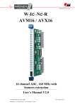
1
Application Note (AN203) PCI-EK01 Register Level Application Guide PCI-EK01 Register Level Application Guide (Ver1.1) Windows, Windows2000, Windows NT and Windows XP are trademarks of Microsoft. We acknowledge that the trademarks or service names of all other organizations mentioned in this document as their own property. Information furnished by DAQ system is believed to be accurate and reliable. However, no responsibility is assumed by DAQ system for its use, nor for any infringements of patents or other rights of third parties which may result from its use. No license is granted by implication or otherwise under any patent or copyrights of DAQ system. The information in this document is subject to change without notice and no part of this document may be copied or reproduced without the prior written consent. Copyrights 2005 DAQ system, All rights reserved. 2005 DAQ system, all rights reserved. http://www.daqsystem.com Application Note (AN203) PCI-EK01 Register Level Application Guide -- Contents -1. PCI BUS Address Space 2. PCI-EK01 Functional Block Diagram 3. I/O Address Usage 4. Memory Address Usage 5. Counter Usage 6. Timer Usage 7. UART Usage 8. VGA Usage 9. ADC Usage 10. DAC Usage 11. Digital I/O(82C55) Usage 12. Interrupt Controller Usage References 2005 DAQ system, all rights reserved. http://www.daqsystem.com Application Note (AN203) PCI-EK01 Register Level Application Guide 1. PCI BUS Address Space As it uses CPU of the x86 system which we use mainly, it can classify greatly it to memory and I/O area. In order to support Plug & Play in case of PCI bus that has a special Configuration. It can save the resource and device state control register etc. 4G Memory Area 64K I/O Area 64DWORD Configuration Area The PCI-EK01 use a memory and I/O that have been assigned to system for operation, the contents are as follows that they required. Address Area Requirements Memory Maximum 64MByte I/O 256 Byte Configuration 128 Byte 2005 DAQ system, all rights reserved. Remark http://www.daqsystem.com Application Note (AN203) PCI-EK01 Register Level Application Guide 2. PCI-EK01 Functional Block Diagram An area of assigned address in PCI-EK01 is used like Figure 3-3. All peripheral device’s control and status register located in I/O area, only high speed SRAM located in memory area. This can not be used in most applications because of allocation of resources for the system at boot time only in Configuration area. PCI BUS Local BUS PCI-EK01 INTERNAL BLOCK - FPGA Local Bus Address Data(Mem,I/O) Counter 0 (0x0) Counter 1 (0x10) PCI Target Counter 2 (0x20) Timer 0 (0x30) Timer 1 (0x40) BUS Mux Timer 2 (0x50) MEM Decoder To each IO Module IO Decoder UART (0x60) FIFO VGA (0x70) DPRAM ADC (0x80) CLOCK syn. DAC (0x90) IO(82C55) (0xa0) Interrupt Controler (0xb0) Ext. Address, Data, Control INT sources in Chip MEM Decoder From Ext. [Note] PCI-EK01(A) don’t have these functions In the above picture, PCI-EK01 (A / B) is represented by the function block, and dotted lines feature of PCI-EK01 (A) has not been implemented yet. (Notice) UART or VGA functionality is available for future upgrades. 2005 DAQ system, all rights reserved. http://www.daqsystem.com Application Note (AN203) PCI-EK01 Register Level Application Guide 3. I/O Address Usage The below table, the address of the I / O area indicates the base address of the peripheral device. All I / O registers are 32-bit input / output processing. I/O Address Offset Base Function Description Comment 00h Counter 0 32bit counter 0 10h Counter 1 32bit counter 1 PCI-EK01(B) Only 20h Counter 2 32bit counter 2 PCI-EK01(B) Only 30h Timer 0 32bit Timer 0 40h Timer 1 32bit Timer 1 PCI-EK01(B) Only 50h Timer 2 32bit Timer 2 PCI-EK01(B) Only 60h UART Universal asynchronous receiver transmitter (RS232C) PCI-EK01(B) Only 70h VGA VGA Display PCI-EK01(B) Only 80h ADC Analog to Digital converter 90h DAC Digital to Analog converter A0h I/O (8255) Digital Input/Output (82C55) B0h Interrupt Interrupt controller B0h-FFh Reserved Reserved space for future upgrade 4. Memory Address Usage Only high speed SRAM is located in the memory area, memory area is always 32-bit input/output. The memory is 32-bit processing in the PCI-EK01(A), the lower 16-bit is only memory value, the upper 16-bit is only displayed “0”. PCI-EK01(B) is 32-bit. Memory read / write can operate up to maximum 33M cycles. Memory Address Space Model 0h - 100000h PCI-EK01(A) 16Bit Bus width (High 16bit space is not used) Total 512K Byte 0h - 100000h PCI-EK01(B) 32Bit Bus width Total 1M Byte Description 2005 DAQ system, all rights reserved. Comment http://www.daqsystem.com Application Note (AN203) PCI-EK01 Register Level Application Guide 5. Counter Usage PCI-EK01 can use three 32-bit counter, can be reduced the overhead of the program in 16bitcounter. The counter is increased rising edge of the counter (LOW -> HIGH Transition), the interface is a 3.3V CMOS logic levels. The maximum count frequency is 20Mhz. I/O Address Offset Function Counter 0 Counter 1 Counter 2 Register Description 00h CNT_CUR Current 32bit counter value 04h CNT_TAR Target 32bit counter value 08h COMMAND Counter Control Command 0Ch STATUS Counter Operation Status 10h CNT_CUR Current 32bit counter value 14h CNT_TAR Target 32bit counter value 18h COMMAND Counter Control Command 1Ch STATUS Counter Operation Status 20h CNT_CUR Current 32bit counter value 24h CNT_TAR Target 32bit counter value 28h COMMAND Counter Control Command 2Ch STATUS Counter Operation Status (1) CNT_CUR Save the current 32-bit counter value. Init. Value : 0x00000000h (2) CNT_TAR The user set up 32-bit Counter value. If set the counter value is greater than or equal to the current value, a bit of the STATUS register will be displayed. Init. Value : 0xFFFFFFFFh (3) COMMAND Counter COMMAND Register Bit Position & Usage 31 2 Reserved Bit Name 0 Enable 1 Clear 1 0 Use Description Default Value In case of ‘1’, should be Counter operation. ‘0’ In case of ‘1’, the CNT_CUR value initialize ‘0’ 0x00000000h. 31 - 2 Reserved For future use 2005 DAQ system, all rights reserved. All ‘0’ http://www.daqsystem.com Application Note (AN203) PCI-EK01 Register Level Application Guide (4) STATUS Counter STATUS Register Bit Position & Usage 31 2 Reserved 1 0 Use Bit Name Description Default Value 0 CNT_IN External counter pin indicates current port External status value. 1 Over CNT_CUR value is greater than or equal to ‘0’ CNT_TAR value, it will be ‘1. 31 - 2 Reserved For future use 2005 DAQ system, all rights reserved. All ‘0’ http://www.daqsystem.com Application Note (AN203) PCI-EK01 Register Level Application Guide 6. Timer Usage PCI-EK01 can use the three 32-bit Timer. The timer use 50MHz clock on the board, the resolution can be set in units 20nSEC. Therefore, from the minimum 40nSEC up to maximum 85,899,345,900nSEC (about 86 seconds) can be set. Function Timer 0 Timer 1 Timer 2 I/O Address Offset Register Description 30h TMR_CUR Current 32bit Timer value 34h TMR_SET Setted 32bit Timer value 38h COMMAND Counter Control Command 3Ch STATUS Counter Operation Status 40h TMR_CUR Current 32bit Timer value 44h TMR_SET Setted 32bit Timer value 48h COMMAND Counter Control Command 4Ch STATUS Counter Operation Status 50h TMR_CUR Current 32bit Timer value 54h TMR_SET Setted 32bit Timer value 58h COMMAND Counter Control Command 5Ch STATUS Counter Operation Status (1) TMR_CUR The current 32-bit Timer value is stored. The Counter is Down Counter. If all bit is “0”, a timeout occurs. This can be found in the status register. Init. Value : 0x00000000h (2) TMR_SET The user set the 32-bit Timer value. Set the Timer value is loaded to TMR_CUR register. When a time out, output is reversed (ALT = 0) in Auto-reload mode. Represents in terms of frequency, are as follows: Frequency = 25M / (TMR_SET + 1) When a time out, output is 20nSEC pulse (ALT = 1) in Auto-reload mode. Represents in terms of frequency, are as follows: Frequency = 50M / (TMR_SET + 1) The TMR_SET value should be at least one or more. Init. Value : 0xFFFFFFFFh 2005 DAQ system, all rights reserved. http://www.daqsystem.com Application Note (AN203) PCI-EK01 Register Level Application Guide (3) COMMAND Counter COMMAND Register Bit Position & Usage 31 8 7 6 5 Reserved Bit Name 0 Enable 1 Clear 4 3 2 1 0 Used Description Default Value If it is ‘1’, the Timer operates. (Down Counter) ‘0’ If it is ‘1’, the TMR_CUR value initializes ‘0’ 0x00000000h. 2 Auto If it is ‘1’, the Timer value automatically reload ‘0’ the TMR_SET value when the timer occurs time-out. 3 Alt If it is ‘0’, the time-out output value will be ‘0’ inverted in every time time-out occurs. If it is ‘1’, 20nSEC High Active Pulse is caused to Timer output when time-out occurs. 4 OutSel If it is ‘1’, the time-out output can be used as ‘0’ the general I/O, and this time output is OutVal”. If it is ‘0’, send the one-shot or reversed output with depending on the timer value. 5 OutVal ‘0’ It is an output value when the time-out output can be used as the general I/O. 6 Reserved 7 Load For future use ‘0’ If it is ‘1’, the TMR_SET value will be loaded to ‘0’ TMR_CUR value. If it is ‘0’, the Timer can operate when the timer “Enable” set value is ‘1’. 31 - 8 Reserved For future use 2005 DAQ system, all rights reserved. All ‘0’ http://www.daqsystem.com Application Note (AN203) PCI-EK01 Register Level Application Guide (4) STATUS Counter STATUS Register Bit Position & Usage 31 1 Reserved 0 Use Bit Name Description Default Value 0 TimeOut When time-out occurs(TMR_CUR value is ‘0’), ‘1’ it will be ‘1’. 31 - 1 Reserved For future use 2005 DAQ system, all rights reserved. All ‘0’ http://www.daqsystem.com Application Note (AN203) PCI-EK01 Register Level Application Guide 7. UART Usage This feature is not currently implemented, it will be supported to PCI-EK01 (B) model. Function UART I/O Address Offset Register Description 60h Register 0 For future use 64h Register 1 For future use 68h Register 2 For future use 6Ch Register 3 For future use 2005 DAQ system, all rights reserved. http://www.daqsystem.com Application Note (AN203) PCI-EK01 Register Level Application Guide 8. VGA Usage This feature is not currently implemented, it will be supported to PCI-EK01 (B) model. Function VGA I/O Address Offset Register Description 70h Register 0 For future use 74h Register 1 For future use 78h Register 2 For future use 7Ch Register 3 For future use 2005 DAQ system, all rights reserved. http://www.daqsystem.com Application Note (AN203) PCI-EK01 Register Level Application Guide 9. ADC Usage PCI-EK01 has 8 SE(Single Ended) ADC(Analog to Digital Converter) channels. If it use Differential method, it can be used 4 channels. The maximum sampling speed is 200Ksps, the input range is different to depending on the options, the value is from 0 to Vref or from –Vref/2 to +Vref/2, Vref value is 2.5V, it can select 3.3V. A resolution is 12-bit. READ POINTER, ADC_PRD, TRG_POS, TRG_LEVEL, CH_SEL0, CH_SEL1, CH_SEL2, CH_SEL3 is located in the same I/O address, however it can be accessed differently depending on the reg_sel value of COMMAND register. Function ADC I/O Address Offset Register Description 80h DATA 32Bit ADC data (Read/Write) 84h COMMAND ADC Control command Register (Read/Write) 88h READ POINTER ADC FIFO READ Pointer (Read only) reg_sel = “000” 88h ADC_PRD ADC sampling period register(Read/Write) reg_sel = “001” 88h TRG_POS Read H/W Trigger position (Read only) reg_sel = “010” 88h TRG_LEVEL Set H/W Trigger level (Read/ Write) reg_sel = “011” 88h CH_SEL0 ADC Channel Select register 0(Read /Write) reg_sel = “100” 88h CH_SEL1 ADC Channel Select register 1(Read / Write) reg_sel = “101” 88h CH_SEL2 ADC Channel Select register 2(Read /Write) reg_sel = “110” 88h CH_SEL3 ADC Channel Select register 3(Read / Write) reg_sel = “111” 8Ch STATUS ADC Status register (Read only) reg_sel = “00” 8Ch READ POINTER Set FIFO READ point Address (Write only) (1) DATA The data value written to the data register directly control the ADC chip which is connected 16-bit data bus of ADC chip through local bus on the board. All I/O and memory access of PCI-EK01 is 32-bit, but upper 16-bit don’t use it. When the ADC chip was controlled by the manual, ADC internal register can control to refer chip manual. The most used command is 0xE010, this is command to convert to the SE mode for 0 channel. After the conversion, when a read operation on DATA register, ADC conversion value can be read. Refer to chip (AD7859AS) manual for more information. ADC Data Register Bit Position & meaning 31 16 Reserved 15 14 13 12 11 10 9 D15 8 7 6 ADC Data Bus 5 4 3 2 1 0 D0 If you use an ADC chip as the manual, the Manual bit of COMMAND register should be set '1. 2005 DAQ system, all rights reserved. http://www.daqsystem.com Application Note (AN203) PCI-EK01 Register Level Application Guide (2) COMMAND ADC Command Register Bit Position & meaning 31 16 15 14 13 12 11 10 9 Reserved Bit Name 0 Manual R TA HC LC TP 8 7 Reg_sel E 6 5 4 TLoad Description 3 2 1 0 A D O M Default Value If it is ‘1’, it control the ADC by Manual. ‘0’ If it is ‘0’, it is Free running <(Notice) 1.> 1 Operation 2 DIFF ‘1’ is Normal mode trigger, ‘0’ is Auto mode ‘0’ If it is ‘1’, it is a Differential mode. If it is ‘0’, it ‘0’ is 3 AMODE a Single Ended mode. Setup the Input Range to Analog mode. ‘0’ Refer to chip manual Trigger pace load “000” 6-4 Trg load 7 Ext External trigger ‘0’ 10-8 Reg sel Register select “000” 11 Trg Pol Register select 아래 <㈜ 2> ‘0’ 12 Low Clear Low RAM full clear(write only) ‘0’ 13 High Clear High RAM full clear(write only) ‘0’ 14 Trg arm Trigger Arm(write only) ‘0’ 15 RESET Initialize the ADC operation. (write only) ‘0’ 31- 16 Reserved For future use All ‘0’ (Notice) 1. Manual bit ADC values that converted to automatic mode are stored high-speed RAM of internal chip. The RAM is composed two 1024WORD(16-bit). So, total 2048 16-bit WORD is stored. If the top-level address of the internal RAM is stored, it is saved by moving to the first address again, the value of the data that was previously recorded will be lost. (Notice) 2. reg_sel By reg_sel value of bit 10-8, reading/writing changes to a specific register at I/O offset address 88h. The table below shows the Register value selected by the reg_sel. For example, to write a value to CH_SEL0, reg_sel record "100". When read/write 88h, read/write to CH_SEL0. 2005 DAQ system, all rights reserved. http://www.daqsystem.com Application Note (AN203) PCI-EK01 Register Level Application Guide Reg_sel Selected Register “000” Read Pointer “001” ADC_PRD “010” TRG_POS “011” TRG_LEVEL “100” CH_SEL0 “101” CH_SEL1 “110” CH_SEL2 “111” CH_SEL3 (3) STATUS ADC indicates the operating status. ADC STATUS Register Bit Position & meaning 31 16 15 14 13 12 11 10 9 Reserved Bit Name 10-0 FIFO Ptr B TD HF LF TA Description Represents the ADC FIFO Pointer.(Read) 8 7 6 5 4 3 2 1 0 ADC FIFO Pointer Default Value ‘0’ Read pointer is set to high-speed RAM. (Write)<(Notice) 1> 11 Trg Arm If it is ‘1’, wait for Trigger occurrence. ‘0’ 12 Low Full If it is ‘1’, full lower-RAM ‘0’ 13 High Full If it is ‘1’, full upper-RAM ‘0’ 14 Trg Done If it is ‘1’, Trigger done ‘0’ 15 Busy If it is ‘1’, represents the ADC operation. ‘0’ 31- 16 Reserved For future use All ‘0’ If it has write operation to the Status register, bits 10-0 of the program by setting the read pointer is to be read in a specific address. 2005 DAQ system, all rights reserved. http://www.daqsystem.com Application Note (AN203) PCI-EK01 Register Level Application Guide (4) CH_SEL0/1/2/3 When ADC operates the Hardware SCAN(AUTO) mode, specific channel that want to get an analog value can convert selectively. This function is available through the Channel Select register. Each Channel Select register store the sampling channel number from 0 to 7. Sample order, is performed repeatedly from SAM_CH0 to SAM_CH7. Currently, only the lower three bits of each sample channel is used. ADC CH_SEL0 Register Bit Position & meaning 31 16 15 14 13 12 11 10 9 Reserved 8 7 6 5 SAM_CH1 4 3 2 1 0 2 1 0 2 1 0 2 1 0 SAM_CH0 ADC CH_SEL1 Register Bit Position & meaning 31 16 15 14 13 12 11 10 9 Reserved 8 7 6 5 SAM_CH3 4 3 SAM_CH2 ADC CH_SEL2 Register Bit Position & meaning 31 16 15 14 13 12 11 10 9 Reserved 8 7 6 5 SAM_CH5 4 3 SAM_CH4 ADC CH_SEL3 Register Bit Position & meaning 31 16 15 14 13 12 11 10 9 Reserved SAM_CH7 8 7 6 5 4 3 SAM_CH6 The structure of the 8-bit hardware SAM_CH indicates the channel number. In SE mode bit 0-2 means three bits, and bits 7-3 are available for up to add future capabilities. In Differential mode, bits 0 and 1 is meaningful only shows the channel number. For example, if you want to convert the hardware channel only 0 and 6, SAM_CH0/2/4/6 will be written to “0”, SAM_CH1/3/5/7 will be written to “6”. If you want to convert all of the channels, each SAM_CH will be written channel numbers that want to convert. The conversion order follow in order to record the number. 2005 DAQ system, all rights reserved. http://www.daqsystem.com Application Note (AN203) PCI-EK01 Register Level Application Guide (5) ADC Read Pointer Converted Chip ADC value is stored in the high-speed RAM. Two high-speed RAM size is 1K 16-bit words. (Previously method stored in the external RAM is not used in version 1.1.) There are continuously sampling in version 1.1, to read the ADC address value can be known the ADC read pointer, to write the ADC pointer can be known the Status register. ADC Read Pointer 31 11 10 9 8 Reserved 7 6 5 4 3 2 1 2 1 0 Read Pointer address (6) ADC_PRD ADC Sampling period register Bit Position & meaning 31 16 Reserved 15 14 13 12 11 10 9 D15 8 7 6 5 4 3 Sampling Period Value 0 D0 The maximum conversion rate of the ADC is 200KSPS (5uSEC cycle). If the ADC_PRD value of 0/1, it is successively ADC conversion by the maximum speed. However, if ADC_PRD has a another value than not ‘0’ or ‘1’, it can be used by decreasing sampling speed(period). In case of ‘2’, sampling period is 7.5uSEC, in case of ‘3’, sampling period is 10uSEC, the sampling period represented by the equation is as follows: Sampling Period = 5.0uSEC + (ADC_PRD-1) x 2.5uSEC When the ADC_PRD values 0 and 1, the maximum sampling period of the exception is 5.0uSEC. (7) Trigger position When H/W Trigger occurs, ADC address value is stored. (Future Function) ADC Trigger position Register 31 11 10 9 Reserved 2005 DAQ system, all rights reserved. 8 7 6 5 4 3 2 1 0 H/W Trigger position http://www.daqsystem.com Application Note (AN203) PCI-EK01 Register Level Application Guide (8) Trigger control H / W trigger level can be set. (Future Function) ADC Trigger Level Register 31 16 15 14 13 12 11 10 9 Reserved Bit 11-0 SL TRG_CH Name Trigger 8 7 6 5 4 3 2 1 0 H/W Trigger position Description Default Value ‘0’ Set the trigger level. Level 14-12 TRG ch 15 Slope “000” Set the channel of the trigger. If it is ‘0’, it is a rising edge. If it is ‘1’, it is a ‘0’ falling edge. 31-16 Reserved For future upgrade 2005 DAQ system, all rights reserved. All ‘0’ http://www.daqsystem.com Application Note (AN203) PCI-EK01 Register Level Application Guide 10. DAC Usage PCI-EK01 has 4 DAC(Digital to Analog Converter). The maximum update speed is 1M sapling/sec, output range is form 0 to 3.3V, a resolution is 12-bit. It has 1K word 16-bit FIFO for Waveform Generation function. Function DAC I/O Address Offset Register Description 90h DATA 32Bit DAC data 94h COMMAND DAC Control command Register 98h DIV_VAL DAC auto-reload interval value 9Ch LIMIT_ADDR DAC auto-reload buffer limit address(Write only) 9Ch STATUS DAC operation status Register(Read only) (1) DATA Data values that are written to the data register can be used Waveform generation in the automation mode by automatically written to the internal DAC output FIFO. DAC Data Register Bit Position & meaning 31 16 Reserved 15 14 13 12 11 10 9 A1 A0 PD LD D11 8 7 6 5 4 DAC DATA 3 2 1 0 D0 DAC DATA : DAC data of 12-bit resolution LD : Low Active Load ADC. In other words, if it is ‘1’, simply store the value of the data in the DAC buffer. If it is ‘0’, the value in the buffer outputs to the DAC. Thus, three DAC buffer record the value, if the record at the same time the last to ‘1’, four DAC value can be output. PD : Low Active Power Down. In other words, if it is ‘0’, the DAC is a low-power mode. In normal operation it should be always '1. A1/A0 : It is an address to select one of the four DAC. A1 A0 DAC Output 0 0 DAC 0 0 1 DAC 1 1 0 DAC 2 1 1 DAC 3 In read operation, it represents the value of the FIFO. For more information, refer to chip(AD5324) manual. 2005 DAQ system, all rights reserved. http://www.daqsystem.com Application Note (AN203) PCI-EK01 Register Level Application Guide (2) COMMAND DAC Command Register Bit Position & meaning 31 7 Reserved 6 M 3 Reserved 2 1 0 R I A Bit Name Description Default Value 0 Auto If it is ‘1’, Waveform generation works. (Down ‘0’ Counter) At this time, DAC value uses the internal FIFO. 1 Int_en If it is ‘1’, Interrupt Enable works. ‘0’ When internal FIFO address value reaches the Limit value, Interrupt is generated. (Applied later, It should be set always ’0’.) 2 Reset If it is ‘1’, it initializes the DAC. If it is ‘0’, it ‘0’ makes the normal operation mode. When reset, there was no change internal FIFO value, but you can record DAC value from the beginning because of initialization of FIFO pointer. 6-3 Reserved 7 Manual “1111” For future use If it is ‘1’, the value of DAC can be set for each ‘1’ channel by manual. (Refer to Data Register) 31 - 8 Reserved All ‘0’ For future use [Reference] If Divide is ‘0’, the period of DAC update is 1uSEC. If it is ‘1’, it depends on DIV_VAL value. (Notice) If the actions were changed from automatic mode to manual mode, the reset operation must be once operation. (3) DIV_VAL If DIV_VAL is ‘0’, the period is 2uSEC. If it is ‘1’, it is 4uSEC. If it is ‘2’, it is 6uSEC. If it is ‘3’, it is 8uSEC. That way, it represents equation, update cycle is 2uSEC x (DIV_VAL + 1). DAC DIV_VAL Register Bit Position & meaning 31 16 Reserved 15 14 13 12 11 10 9 D11 8 7 6 Divide Value 5 4 3 2 1 0 D0 Init. Value : 0x0000h 2005 DAQ system, all rights reserved. http://www.daqsystem.com Application Note (AN203) PCI-EK01 Register Level Application Guide (4) LIMIT_ADDR If you create the Waveform by using internal FIFO, a specific address should be move first address in order to make any periodic Waveform. Limit Address are to be used for this. In other words, if you only create a waveform at FIFO address from 0 to 233, and then LIMIT_ADDR value records 233, after that the DAC will be output only to address 233 and move to the first address 0. DAC LIMIT_ADDR Register Bit Position & meaning 31 10 Reserved 9 8 A9 7 6 5 4 3 2 1 FIFO Address limit value 0 A0 Init. Value : 0x3E7h (999d) (5) STATUS DAC STATUS Register Bit Position & meaning 31 10 Reserved 9 A9 8 7 6 5 4 3 2 1 FIFO Addess 0 A0 Bit Name Description Default Value 9-0 FIFO Represents the 10-bit FIFO address. If Auto bit All ‘0’ Address of COMMAND register is ‘0’, it represents the Write address. If it is ‘1’, it represents the Read address (ADC output value). 31-10 Reserved For future use 2005 DAQ system, all rights reserved. All ‘0’ http://www.daqsystem.com Application Note (AN203) PCI-EK01 Register Level Application Guide 11. Digital I/O(82C55) Usage PCI-EK01's Digital Input / Output functions are implemented using the 82C55. In case of the 82C55, the peripheral device control chip of early Intel x86 family have been used. Function I/O(82C55) I/O Address Offset Register Description A0h PORTA 82C55 Port A Register A4h PORTB 82C55 Port B Register A8h PORTC 82C55 Port C Register ACh CONTROL 82C55 Control Register (Write Only) To control the 82C55 port, it must be all setup through the control register. For all setup, the most significant bit will be set to “1” and writes to the control register. If the most significant bit is “0”, it is a command of PORTC bit description. (For more information, refer to 82C55 manual) When the first power, all port will be input and the operation mode will be “0”. 2005 DAQ system, all rights reserved. http://www.daqsystem.com Application Note (AN203) PCI-EK01 Register Level Application Guide 12. Interrupt Controller Usage PCI-EK01 has the interrupt controller for each I/O device by using hardware. When you use these interrupts, overhead of the process can be reduced. Function INTERRUPT I/O Address Offset Register Description B0h INT_STA Interrupt Status Register (Read)/ Interrupt Status Clear (Write) B4h INT_SEL Interrupt Select(Read/Write) B8h INT_EN Interrupt Enable Register (Read/Write) BCh INT_SRC Interrupt Source Indicatior(Read Only) To control the 82C55 port, it must be all setup through the control register. For all setup, the most significant bit will be set to “1” and writes to the control register. If the most significant bit is “0”, it is a command of PORTC bit description. (For more information, refer to 82C55 manual) When the first power, all port will be input and the operation mode will be “0”. (1) INT_STA (Interrupt Status) Indicates devices that are currently required Interrupt. To appear in the status register will have to make the handle. (Read) The Status bit(INT_STA) of each devices that require the Interrupt are eliminated.(Write) The interrupt handling device that requires a bit of a write operation must be one and the corresponding status bit is cleared (Edge-triggered Interrupt). For level-triggered interrupt, request for each device must be cleared directly. INTERRUPT Status Register Bit Position & meaning 31 16 Reserved 15 14 13 12 11 10 9 G S14 8 7 6 5 4 3 2 Status 1 0 S0 Bit Name Description Default Value 0 Counter 0 If it is ‘1’, the Counter 0 requests the Interrupt ‘0’ processing. 1 Counter 1 If it is ‘1’, the Counter 1 requests the Interrupt ‘0’ processing. 2 Counter 2 If it is ‘1’, the Counter 2 requests the Interrupt ‘0’ processing. 3 Timer 0 If it is ‘1’, the Timer 0 requests the Interrupt ‘0’ processing. 4 Timer 1 If it is ‘1’, the Timer 1 requests the Interrupt 2005 DAQ system, all rights reserved. ‘0’ http://www.daqsystem.com Application Note (AN203) PCI-EK01 Register Level Application Guide processing. 5 Timer 1 If it is ‘1’, the Timer 2 requests the Interrupt ‘0’ processing. 6 UART Reserved ‘0’ 7 VGA Reserved ‘0’ 8 ADC Reserved ‘0’ 9 DAC Reserved ‘0’ 10 8255 Reserved ‘0’ 11 Interrupt Reserved ‘0’ 12 EXT0 Reserved ‘0’ 13 EXT1 Reserved ‘0’ 14 EXT2 Reserved ‘0’ 15 Global When any of the above Interrupt sources need ‘0’ to process, it will be changed “1”. 31-16 Reserved All ‘0’ For future use When the interrupt processing ends, the interrupt status bit for each corresponding bit should be cleared. After the bit that want to be cleared write “1”, the Interrupt status of corresponding bit is cleared. After the bit that want to be cleared writes “1”, the Interrupt status of corresponding bit is cleared. Bit 15 is reset (Reset), so all status bits are cleared at the same time. (2) INT_SEL Determines whether to an edge-triggered or level triggered interrupt for each device that requires the interrupt processing. INTERRUPT Select Register Bit Position & meaning 31 16 15 14 13 12 11 10 9 Reserved M14 8 7 6 5 4 3 2 1 Interrupt Mode 0 M0 The Interrupt mode selects until from bit 0 to 14. If it is ‘0’, it is a Level Trigger. If it is ‘1’, it is a Edge trigger. All bit is ‘0’ by default. 2005 DAQ system, all rights reserved. http://www.daqsystem.com Application Note (AN203) PCI-EK01 Register Level Application Guide (3) INT_EN Each Interrupt source is to enable the Interrupt. INTERRUPT Enable Register Bit Position & meaning 31 16 Reserved 15 14 13 12 11 10 9 G E14 8 7 6 5 4 3 2 1 Enable 0 E0 If each bit is ‘1’, it is enabled the device Interrupt of corresponding bit. Because bit 15 is the Global Interrupt Enable bit, This bit is set '1' to enable all Interrupts. (4) INT_SRC INT_STA register represents that each interrupt request output of the device is latched at the rising edge of the signal. Thus, it is the display of Edge triggered rather than Level triggered. Therefore, it requests and cleares the Interrupt. On the other hand, INT_SRC represents that the state of the current output request Interrupt device. INTERRUPT Source Indicator Bit Position & meaning 31 15 14 13 12 11 10 9 Reserved S14 2005 DAQ system, all rights reserved. 8 7 6 5 Interrupt Source 4 3 2 1 0 S0 http://www.daqsystem.com Application Note (AN203) PCI-EK01 Register Level Application Guide References 1. AD7859 Data Sheets Rev. A -- Analog Device, Inc 2. AD5304/5314/5324 Data Sheets Rev. D -- Analog Device, Inc 3. PCI-EK01(A/B) User’s Manual -- DAQ system 4. 82C55 chip manual -- Intel corp. 2005 DAQ system, all rights reserved. http://www.daqsystem.com