1
RTE-VR5432-CB
USER’S MANUAL (Rev. 2.01)
Midas lab
RTE-VR5432-CB
USER’S MANUAL (Rev. 2.01)
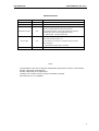
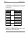
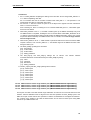
REVISION HISTORY
Date
Revision
August 15, 1999
1.00
Official 1st edition
Explanation of revision
September 15, 1999
1.01
Modification of current consumption from 2.5A (max.) to 2.0A (max.)
Change accompanied by specification change (specification change
of the bus in Big Endian) for H/W version Rev.2.00
December 29,1999
2.00
The chapter and section which were changed are as follows.
The description part concerning BigEndian to each.
7.3 Address Map
9 ROM Programming
Clerical error correction
5.16 CPU Connectors (JCP1, 2)
April 12,2000
2.01
… The maker of a connector is corrected to hirose from KEL.
10.3 Chip Select
… Logical address range value is corrected.
Notes
The specification in the case of using RTE-VR5432-CB by Big Endian in H/W Rev.2 was changed.
H/W Rev.1:Byte-Swap is implemented.
H/W Rev.2:Byte Swap is not implemented.
Therefore, how to write in access to I/O space and ROM is changed.
About this point, it is not compatible.
ii
RTE-VR5432-CB
USER’S MANUAL (Rev. 2.01)
CONTENTS
1.
INTRODUCTION........................................................................................................................... 1
1.1.
NUMERIC NOTATION ..................................................................................................... 1
2.
FUNCTIONS ................................................................................................................................. 2
3.
MAJOR FEATURES ..................................................................................................................... 3
4.
BASIC SPECIFICATIONS............................................................................................................ 3
5.
BOARD CONFIGURATION.......................................................................................................... 4
5.1.
RESET SWITCH (SW_RESET) ....................................................................................... 4
5.2.
POWER CONNECTOR (JPOWER)................................................................................. 4
5.3.
SWITCH 1 (SW1) ............................................................................................................. 4
5.4.
SWITCH 2 (SW2) ............................................................................................................. 5
5.5.
SWITCH 3 (SW3) ............................................................................................................. 5
5.6.
SWITCH 4 (SW4) ............................................................................................................. 6
5.7.
SWITCH 5 (SW5) ............................................................................................................. 6
5.8.
7SEG-LED, XXX-LED ...................................................................................................... 6
5.9.
CLOCK SOCKET (OSC1) ................................................................................................ 7
5.10. ROM SOCKETS ............................................................................................................... 7
5.11. SERIAL CONNECTOR (JSIO1, JSIO2) ........................................................................... 7
5.12. PARALLEL CONNECTOR (JPRT) .................................................................................. 8
5.13. ROM EMULATOR TEST PIN (JROM-EML) .................................................................... 8
5.14. ICE CONNECTOR (JDCU) ............................................................................................. 9
5.15. JGBUS CONNECTOR (JGBUS)...................................................................................... 9
5.16. CPU CONNECTORS (JCP1, 2) ..................................................................................... 10
6.
CONNECTION WITH THE HOST PC......................................................................................... 11
6.1.
RS-232C CONNECTION ............................................................................................... 11
7.
HARDWARE REFERENCES ..................................................................................................... 12
7.1.
RESET 12
7.2.
INTERRUPTS................................................................................................................. 12
7.3.
ADDRESS MAP ............................................................................................................. 13
7.3.1. SRAM Space (0000-0000H to 07FF-FFFFH).................................................... 13
7.3.2. DRAM Space (0800-0000H to 0FFF-FFFFH) ................................................... 13
7.3.3. GBUS Space (1000-0000H to 17FF-FFFFH).................................................... 13
7.3.4. I/O Space (1800-0000H to 1EFF-FFFFH)......................................................... 14
7.3.5. ROM Space (1F00-0000H to 1FFF-FFFFH) ..................................................... 14
7.4.
I/O DETAILS................................................................................................................... 15
7.4.1. SRAM Controller (SRAMC B800-6000[Read/Write]) ........................................ 15
7.4.2. DRAM Controller (DRAMC B800-5000[Read/Write])........................................ 16
7.4.3. DRAM Initialization Port (DRAM_INIT B800-4000H[Write Only]) ..................... 18
7.4.4. SW1 Read Port (SW1 B800-0000H [Read Only]) ............................................. 18
7.4.5. SW2 Read Port (SW2 B800-1000H [Read Only]) ............................................. 19
7.4.6. 7-Segment LED Display Data Output Port (7SEG-LED B800-2000 [Write Only])
iii
RTE-VR5432-CB
7.4.7.
7.4.8.
7.4.9.
7.4.10.
USER’S MANUAL (Rev. 2.01)
19
Serial/parallel I/O (SCC0/1 LPT B900-1000 to B900-4000[Read/Write]).......... 20
Timer (Timer B900-5000[Read/Write]) .............................................................. 21
Interrupt Controller (PIC B900-0000[Read/Write]) ............................................ 22
DMA Controller .................................................................................................. 23
8.
BUS CYCLE TIMING.................................................................................................................. 27
8.1.
SRAM ACCESS ............................................................................................................. 27
8.2
DRAM ACCESS ............................................................................................................. 29
8.3.
LOCAL BUS ACCESS ................................................................................................... 32
8.4.
LIST OF REQUIRED CLOCKS ...................................................................................... 34
8.4.1. SRAM Access.................................................................................................... 34
8.4.2. SDRAM Access ................................................................................................. 34
9.
ROM PROGRAMMING............................................................................................................... 35
9.1
INITIALIZATION ............................................................................................................. 35
9.2
ROM DATA ASSIGNMENT............................................................................................ 35
10. SPECIFIC GBUS SPECIFICATIONS ......................................................................................... 36
10.1
OVERVIEW .................................................................................................................... 36
10.2
BUS CYCLE ................................................................................................................... 37
10.3
CHIP SELECT ................................................................................................................ 38
11. APPENDIX A MULTI MONITOR ............................................................................................... 39
11.1. BOARD SETTING .......................................................................................................... 39
11.1.1. RTE for Win 32 Installation................................................................................ 39
11.1.2. SW1 Setting....................................................................................................... 39
11.1.3. Connection of Board.......................................................................................... 39
11.2. MULTI MONITOR........................................................................................................... 40
11.2.1. 7-Segment LED on Startup ............................................................................... 40
11.2.2. Monitor Work RAM ............................................................................................ 40
11.2.3. Interrupt ............................................................................................................. 40
11.2.4. _INIT_SP Setting............................................................................................... 40
11.2.5. Timer Interrupt ................................................................................................... 40
11.2.6. Initializing Hardware .......................................................................................... 41
11.2.7. Special Instruction ............................................................................................. 41
11.3. RTE COMMANDS .......................................................................................................... 41
11.3.1. HELP(?) ............................................................................................................. 41
11.3.2. INIT .................................................................................................................... 41
11.3.3. VER ................................................................................................................... 41
11.3.4 CACHEFLUSH .................................................................................................. 41
11.3.5 SHOWTLB ......................................................................................................... 42
11.3.6 IOREAD ............................................................................................................. 42
11.3.7 IOWRITE ........................................................................................................... 42
12. APPENDIX B PARTNER MONITOR......................................................................................... 43
12.1. BOARD SETTING .......................................................................................................... 43
12.1.1. SW1 Setting....................................................................................................... 43
12.1.2. Connection of Board.......................................................................................... 43
12.2
PARTNER MONITOR .................................................................................................... 44
iv
RTE-VR5432-CB
12.2.1.
12.2.2.
12.2.3.
12.2.4.
12.2.5.
12.2.6.
12.2.7.
USER’S MANUAL (Rev. 2.01)
7-Segment LED on Startup ............................................................................... 44
ROM Monitor Work RAM................................................................................... 44
Interrupt ............................................................................................................. 44
INIT_SP Setting................................................................................................. 44
Remote Connection........................................................................................... 44
Initializing Hardware .......................................................................................... 45
Special Instruction ............................................................................................. 45
13. APPENDIX C INTERRUPT PROGRAMMING .......................................................................... 46
13.1. INTERRUPT LIBRARY................................................................................................... 46
13.1.1. int InitlrqVect(void) ............................................................................................. 46
13.1.2. int TermlrqVect(void) ......................................................................................... 46
13.1.3. int SetlrqVect(int no, int func) ............................................................................ 46
13.1.4. int GetlrqVect(int no).......................................................................................... 46
13.1.5. void SetlPnBit(int IPn)........................................................................................ 46
13.1.6. void ReslPnBit(int IPn)....................................................................................... 46
13.1.7. void ei(void) ....................................................................................................... 46
13.1.8. void di(void) ....................................................................................................... 46
13.2. INTERRUPT ROUTINE.................................................................................................. 46
13.3. SAMPLE PROGRAM ..................................................................................................... 47
14. APPENDIX C GBUS COMMON SPECIFICATIONS................................................................. 48
14.1. TERMINOLOGY............................................................................................................. 48
14.1.1. CPU Board and Motherboard ............................................................................ 48
14.1.2. Bus Cycle and Micro Cycle................................................................................ 48
14.2. SIGNALS ........................................................................................................................ 48
14.3. PIN ASSIGNMENTS ...................................................................................................... 53
14.4. PROCESSING OF UNUSED PINS................................................................................ 54
14.5. ALLOCATING GCS-[7:0]................................................................................................ 54
14.6. BUS CYCLE ................................................................................................................... 55
14.6.1. Single Cycle....................................................................................................... 55
14.6.2. Burst Cycle ........................................................................................................ 55
14.6.3. GWAITI-............................................................................................................. 56
14.6.4. GBTERM- .......................................................................................................... 57
14.7. TIMING58
14.7.1. Setup Time ........................................................................................................ 58
14.7.2. Delay Time......................................................................................................... 58
v
RTE-VR5432-CB
1.
USER’S MANUAL (Rev. 2.01)
INTRODUCTION
The RTE-VR5432-CB is a CPU board that is designed to evaluate the NEC RISC processor.
The board features a VR5432 CPU capable of operating at a maximum speed of 167 MHz, memory,
serial/parallel interface, and bus connector for expansion. As the memories, a high-speed PB-SRAM and
high-capacity SDRAM are provided as standard.
These functions enable the RTE-VR5432-CB to be used for a wide variety of applications including
processor performance evaluation and application program development at the initial stage, and to also be
used as an engine for demonstration and simulation.
The GHS Multi or NEC PARTNER source-level debugger can be used as a development software tool
with the RTE-VR5432-CB. The type of monitor to be stored in ROM depends on the debugger type.
In ROM, the monitor specified at the time of purchase is stored. Even when neither of the debuggers is
purchased together with the RTE-VR5432-CB, they can be purchased at anytime subsequently.
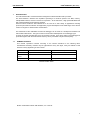
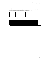
1.1.
NUMERIC NOTATION
This manual represents numbers according to the notation described in the following table.
Hexadecimal and binary numbers may be hyphenated at every four digits, if they are difficult to read
because of many digits being in each number.
Number
Notation rule
Example
Decimal number
Only numerals are indicated.
"10" represents number 10 in decimal.
Hexadecimal
A number is suffixed with letter H.
"10H" represents number 16 in decimal.
A number is suffixed with letter B.
"10B" represents number 2 in decimal.
number
Binary number
Number Notation Rules
Multi is a trademark of Green Hills Software, Inc. in the US.
1
RTE-VR5432-CB
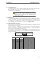
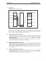
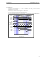
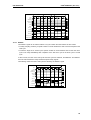
2.
USER’S MANUAL (Rev. 2.01)
FUNCTIONS
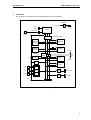
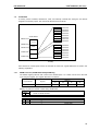
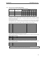
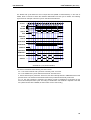
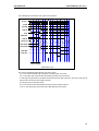
The overview of each function block of the RTE-VR5432-CB is shown below.
DC/DC
3.3V/2.5V
OSC
xxMHz
DC-JACK
5V
VR5432
Mode SW
RESET
SW
JCPU(CPU CONE)
PBSRAM
CONT
PBSRAM
SDRAM
CONT
SDRAM
SYSAD
TIMOUT
GBUS
Bridge
IRQ
CONT
ROM
GBUS
TIM
DMAC
DB9
SCC
DB9
SCC
CN26
PRT
PORT
7SEG-LED
PORT
DIP-SW
C D A
IRQ
GBUS CONE
RTE-VR5432-CB Block Diagram
2
RTE-VR5432-CB
USER’S MANUAL (Rev. 2.01)
3.
MAJOR FEATURES
• Two types of monitor ROM are provided: one is used for the GreenHills Multi and the other for the NEC
PARTNER.
• Real-time execution and evaluation at a high-level language level are possible.
• 256 Kbytes of PB-SRAM and 64 Mbytes of SDRAM are provided as standard.
• Two interfaces are provided: Serial (2 channels) and parallel (IEE1284).
• A ROM emulator and N-Wire tool can be connected.
4.
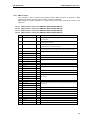
BASIC SPECIFICATIONS
Processor
CPU clock
Bus clock
Power supply
Memory
EPROM
PB-SRAM
SDRAM
I/O
Serial interface
Parallel interface
Timer
I/O port
Others
CPU connector
GBUS connector
Reset switch
VR5432
150 MHz (167 MHz max.)
60 MHz (max.)
+5 V, 2.0 A (max.)
256 KB
256 KB
64 MB
128 K × 16 bits (40-pin DIP) × 1 (512 Kbytes max.)
32 K × 32 bits × 2
4 M × 4 bits × 4 banks × 8
Equivalent to NS16550, DB9 connector × 2 channels
IEEE1284 compatible, CON26 connector
µPD71054, 500-ns resolution
LED (7 segment) display/switch input
Connector connecting all VR5432 pins
RTE-CB compliant 32-bit I/F (4-GB, 32-bit bus, supporting DMA)
Push type
3
RTE-VR5432-CB
5.
USER’S MANUAL (Rev. 2.01)
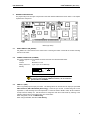
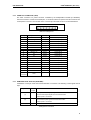
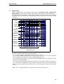
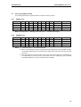
BOARD CONFIGURATION
The physical layout of the major components on the RTE-VR5432-CB board is shown below. This chapter
explains each component.
Board (Top View)
5.1.
RESET SWITCH (SW_RESET)
SW_RESET is a reset switch for the entire board. Pressing this switch causes all the circuits including
the CPU to be reset.
5.2.
POWER CONNECTOR (JPOWER)
The power supplied to the JPOWER connector should be one rated as listed below.
Voltage:
+5 V
Current:
Maximum of 2.0 A
Mating connector: Type A (5.5 mm in diameter)
Polarity:
+5V
GND
GND
+5V
Note the polarity when attaching the power connector.
To supply power from the JGBUS connector, do not connect a
power source to JPOWER.
5.3.
SWITCH 1 (SW1)
SW1 is a general-purpose input port switch. The setting status can be read from an input port (see 7.4.4
SW1 Read Port (SW1 B800-0000H [Read Only])). When the port is read, a switch being set to OFF
represents 1, while its being set to ON represents 0. When the monitor ROM is used, all SW1 switches
except some are already set. Set this switch for assignment with the monitor ROM by referring to the
following sections and in accordance with your environment:
When using Multi, see 11.1.2 SW1 Setting.
When using PARTNER, see 12.1.1 SW1 Setting.
4
RTE-VR5432-CB
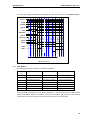
5.4.
USER’S MANUAL (Rev. 2.01)
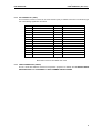
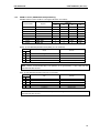
SWITCH 2 (SW2)
SW2 selects an operation of the board by hardware. The setting of the switch can be read from an input
port (see 7.4.5 SW2 Read Port (SW2 B800 to 1000H [Read Only])).
No.
Signal name
Factory setting
1
FBOOT
OFF
Function
Specifies resources to be allocated to the CS0 space.
OFF: The on-board UV-EPROM is allocated to the CS0 space.
ON: GCS1- space of GBUS is allocated to the CS0 space (see
10.3 CHIP SELECT).
2
TEST1
OFF
Set this signal to OFF.
3
BCLK_LOW
OFF
Selects frequency of oscillator mounted on OSC1. Depending on
the value set, the monitor ROM changes the number of ROM and
SRAM wait cycles. In addition, the number of I/O wait cycles is
changed by hardware.
OFF: Bus clock exceeds 33 MHz.
ON:
5.5.
Bus clock is kept at 33 MHz or less.
4
DDDD
OFF
Specifies the write data rate. The Config register of the VR5432
must be set according to the value set here.
OFF: DxxDxxDxxDxx
ON: DDDD
5
TESET2
OFF
Must be set to OFF.
6
Not used
OFF
Must be set to OFF.
7
Not used
OFF
Must be set to OFF.
8
GCLK LOW
OFF
Must be set to OFF.
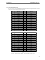
SWITCH 3 (SW3)
SW3 selects the type of ROM inserted in the ROM socket and performs setting related to banks.
No.
Signal name
Factory setting
1
ROM_TYPE0
OFF
2
ROM_TYPE1
OFF
3
BANK_DIS
OFF
Function
Selects the type of ROM.
[ROM_TYPE1, ROM_TYPE0]
[
OFF
,
OFF
]:
[
OFF
,
ON
]:
[
ON
,
OFF
]:
[
ON
,
ON
]:
When monitor ROM is used
When 27C4096 is used
When 27C2048 is used
When 27C1024 is used
Specifies whether the upper and lower halves (banks) of ROM
are separated. Be sure to set this signal to OFF when monitor is
used.
OFF: Upper and lower halves of ROM are separated.
ON: Upper and lower halves of ROM are used as a contiguous
area.
4
Not used
OFF
Must be set to OFF.
5
Not used
OFF
Must be set to OFF.
6
Not used
OFF
Must be set to OFF.
7
MON64
OFF
Specifies the monitor type.
OFF: 32-bit mode
ON: 64-bit mode
8
LITTLE
OFF
Specifies the endian.
OFF: Big endian
ON: Little endian
Remark
If connecting a ROM emulator, set BANK_DIS to ON, and perform the setting to use the
ROMs as a continuous ROM space. (See 9.2 ROM DATA ASSIGNMENT)
5
RTE-VR5432-CB
5.6.
USER’S MANUAL (Rev. 2.01)
SWITCH 4 (SW4)
SW4 specifies the mode of a CPU pin. When a signal of this switch is set to OFF, the corresponding
CPU pin is 1; when it is set to ON, the pin is 0.
SW4
DivMode [1..0] Ratio
1
2
ON
ON
0: 2:1
OFF
ON
1:2.5:1
ON
OFF
2: 3:1
OFF
OFF
3: 4:1
Remark (* indicates factory-setting)
*
SW 4-3 is always fixed to OFF.
SW 4-4 is for testing. Always fix it to OFF.
5.7.
SWITCH 5 (SW5)
SW5 physically cuts the board’s signal lines connected to CPU pins. All the switches are factory-set to
ON (connected). The factory setting should be used in normal cases.
No.
5.8.
CPU pin name
Factory setting
1
Not used
OFF
Internally used resource
2
INT2-
ON
GINT1- of GBUS
3
INT3-
ON
GINT2- of GBUS
4
INT4-
ON
GINT3- of GBUS
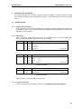
7SEG-LED, XXX-LED
The LEDs are used to indicate statuses, as listed below. The four 7-segment LEDs are used by the
monitor at startup. After that, they can be used for any user application.
LED4
LED3
LED2
Name
POWER
LED1
Description
Lights when power is supplied to the port.
SRAM
Lights during access to the PB-SDRAM space.
DRAM
Lights during access to the SDARM space.
LOCAL
Lights during access to the LOCAL space.
GBUS
Lights during access to the GBUS space.
Board LED Status
6
RTE-VR5432-CB
5.9.
USER’S MANUAL (Rev. 2.01)
CLOCK SOCKET (OSC1)
An oscillator for generating the clock signal to be supplied to the CPU is mounted in the OSC1 socket.
OSC1 is converted to the 3.3-V level, and is connected to the CPUCLK pin of the CPU.
Accepts DIP 8-pin (half-type) oscillators.
When you have to cut an oscillator pin for convenience, be
careful not to cut it too short, or otherwise the frame (housing)
of the oscillator may touch a pin in the socket, resulting in a
short-circuit occurring.
5.10. ROM SOCKETS
The RTE-VR5432-CB has ROM sockets to hold 40-pin ROM chips to provide standard 128 Kbytes (64K
× 16 bits). When the ROM chips used here are to be replaced, their type should be 27C1024, 27C2048,
or 27C4096, and the access time should be 120 ns or less. The SW3 switch must be set again when the
type of ROM is changed or a ROM emulator is connected. (See 5.5 SWITCH3 (SW3))
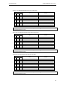
5.11. SERIAL CONNECTOR (JSIO1, JSIO2)
The JSIO1 and JSIO2 connectors are used for the RS-232C interface that is controlled by the serial
controller (TL16C550CPT) on the board.
JSIO1 and JSIO2 are 9-pin D-SUB RS-232C connectors (male) like that commonly used on the PC/AT.
All signals on both of these connectors are converted to the RS-232C level. The figure and table below
indicate the pin and signal arrangement of these connectors.
For the signals to be connected to the host, the table indicates two modes of wiring on the host: one for
a 9-pin D-SUB connector, and the other for a 25-pin D-SUB connector. (Regular cross-cable wiring is
used for these connections.)
1
2
6
3
7
4
8
5
9
Pin Arrangement of JSIO1 and JSIO2
Signal name
Input/
output
1
DCD
Input
2
RxD(RD)
Input
JSIOx pin
Connector pin number on the host side
D-SUB9
D-SUB25
3
2
3
TxD(SD)
Output
2
3
4
DTR(DR)
Output
1, 6
6, 8
5
GND
5
7
6
DSR(ER)
Input
4
20
7
RTS(RS)
Output
8
5
8
CTS(CS)
Input
7
4
9
RI
Input
Connector Signals of JSIO1 and JSIO2
7
RTE-VR5432-CB
USER’S MANUAL (Rev. 2.01)
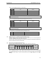
5.12. PARALLEL CONNECTOR (JPRT)
The JPRT connector is a printer connector controlled by the serial/parallel controller (TL16PIR552).
Since the connector consists of 26 header pins, a conversion cable is required to use this connector as a
normal printer connector. The numbers of the connector pins and their functions are described below.
2
4
6
8
10 12 14 16 18 20 22 24 26
1
3
5
7
9
11 13 15 17 19 21 23 25
JPRT Pin Arrangement
JPRT pin
Signal name
Input/output
Remark
1
STB-
Output
10-KΩ pull-up
2
AUTO_FD-
Output
10-KΩ pull-up
3
D0
Output
10-KΩ pull-up
4
ERROR-
Input
10-KΩ pull-up
5
D1
Output
10-KΩ pull-up
6
INIT-
Output
10-KΩ pull-up
7
D2
Output
10-KΩ pull-up
8
SELECT_IN-
Output
10-KΩ pull-up
9
D3
Output
10-KΩ pull-up
11
D4
Output
10-KΩ pull-up
13
D5
Output
10-KΩ pull-up
15
D6
Output
10-KΩ pull-up
17
D7
Output
10-KΩ pull-up
19
ACK-
Input
10-KΩ pull-up
21
BUSY
Input
10-KΩ pull-up
23
PE
Input
10-KΩ pull-up
25
SELECT
Input
10-KΩ pull-up
26
NC
10,12,14,16,
18,20,22,24
Not used
GND
JPRT Connector Signal Table
5.13. ROM EMULATOR TEST PIN (JROM-EML)
JROM-EML is a test pin used when a ROM emulator is connected. The following control signals can be
input.
Signal name
Input/
output
RESET(1)
Input
All the ports are reset by inputting a low level.
Connect reset request signals from the ROM emulator.
Pulled up with 1-KΩ resistor.
NMI-
Input
NMI is input to the CPU by inputting a low level.
Connect NMI request signals from the ROM emulator.
–––
GND. Connect to GND of ROM emulator.
(2)
Function
Pulled up with 1-KΩ resistor.
GND(3)
JROM_EM Pin Functions
8
RTE-VR5432-CB
USER’S MANUAL (Rev. 2.01)
5.14. ICE CONNECTOR (JDCU)
This connector is used to connect an in-circuit emulator (ICE). It enables connection of an RTE-TP type
ICE. The following signals are connected.
Pin No.
Signal name
Pin No.
Signal name
A1
TRCCLK
B1
GND
A2
TRCDATA0
B2
GND
A3
TRCDATA1
B3
GND
A4
TRCDATA2
B4
GND
A5
TRCDATA3
B5
GND
A6
TRCEND
B6
GND
A7
DDI
B7
GND
A8
DCK
B8
GND
A9
DMS
B9
GND
A10
DDO
B10
GND
A11
/DRST
B11
NC.
A12
/BKTGIO
B12
NC.
A13
NC.
B13
+3.3V
JDCU2 Connector Signals
Board-side connector: KEL 8830E-026-170S
5.15. JGBUS CONNECTOR (JGBUS)
This is a 32-bit data width bus connector for expansion purposes. For details, see 10 SPECIFIC GBUS
SPECIFICATIONS and 14 APPENDIX C GBUS COMMON SPECIFICATIONS.
9
RTE-VR5432-CB
USER’S MANUAL (Rev. 2.01)
5.16. CPU CONNECTORS (JCP1, 2)
The CPU connector signals are directly linked to the VR5432. Since these signals are used in the board,
caution is required when pulling out signals from JCPU.
JCPU pin
No.
1
3
5
7
9
11
13
15
17
19
21
23
25
27
29
31
33
35
37
39
41
43
45
47
49
51
Signal name
+5V
SYSAD31
SYSAD29
SYSAD27
SYSAD25
+5V
SYSAD23
SYSAD21
SYSAD19
SYSAD17
+3.3V
SYSAD15
SYSAD13
SYSAD11
SYSAD9
+3.3V
SYSAD7
SYSAD5
SYSAD3
SYSAD1
+2.7V
/NMI
/INT1
/INT3
+2.7V
no use
JCPU pin
No.
2
4
6
8
10
12
14
16
18
20
22
24
26
28
30
32
34
36
38
40
42
44
46
48
50
52
Signal name
GND
SYSAD30
SYSAD28
SYSAD26
SYSAD24
GND
SYSAD22
SYSAD20
SYSAD18
SYSAD16
GND
SYSAD14
SYSAD12
SYSAD10
SYSAD8
GND
SYSAD6
SYSAD4
SYSAD2
SYSAD0
GND
/INT0
/INT2
/INT4
GND
no use
JCPU1 Connector
JCPU pin
No.
1
3
5
7
9
11
13
15
17
19
21
23
25
27
29
31
33
35
37
39
41
43
45
47
49
51
Signal name
+5V
SYSCMD4
SYSCMD2
SYSCMD0
no use
+5V
/EVALID
/EREQ
/EOK
/PREQ
+3.3V
SYSADC3
SYSADC1
SYSCLK2
+3.3V
JTDO
JTCK
TRISTATE
ENDIAN
+2.7V
DIVMODE0
TRCEND
TRCDATA2
TRCDATA0
+2.7V
no use
JCPU pin
No.
2
4
6
8
10
12
14
16
18
20
22
24
26
28
30
32
34
36
38
40
42
44
46
48
50
52
Signal name
GND
SYSCMD3
SYSCMD1
no use
no use
GND
/SYSRESET
/PMASTER
/PVALID
no use
GND
SYSAD2
SYSADC0
no use
GND
JTDI
JTMS
/COLDRESET
no use
GND
DIVMODE1
TRCDATA3
TRCDATA1
/BKTGIO
TRCCLK
no use
JCPU2
Connector: Hirose, board side: FX2-52P-1.27SV, other side: FX2-52S-1.27SV
10
RTE-VR5432-CB
6.
6.1.
USER’S MANUAL (Rev. 2.01)
CONNECTION WITH THE HOST PC
RS-232C CONNECTION
RS-232C connect the host machine using the monitor ROM by means of the following procedure:
<1>
Get an optional RS-232C cable and a power supply.
<2>
Set and check the setting of the switches on the board. Specify a baud rate by using SW1 (see
11.1.2 SW1 Setting and 12.1.1 SW1 Setting).
<3>
Connect the JSIO1 connector and host machine with the RS-232C cable, and supply power to
the JPOWER connector. Confirm that the POWER-LED on the board lights and that the 7segment LED indicating that the monitor has started lights.
If the LED does not light, turn off the power immediately, and
check the connection.
<4>
Start the debugger on the host machine, and connect it via the RS-232C interface. If an error
occurs, confirm the connection of the serial cable and the setting of the switches (especially, baud
rate). For the method and procedure of starting the debugger, see the debugger manual.
Place the board on an insulating material. If a conductive
material touches the board while power is supplied to the
board, the board may malfunction.
11
RTE-VR5432-CB
7.
USER’S MANUAL (Rev. 2.01)
HARDWARE REFERENCES
This chapter describes the hardware of the RTE-VR5432-CB.
7.1.
RESET
Resets are effected by the causes listed below. They are handled as cold reset of the CPU, and result in
system reset of the control circuits on the board.
• Power-on reset: Triggered at power-on of the board.
• Reset switch: Triggered by Reset switch (SW RST) provided on the board.
• GBUS reset: Reset request from the JGBUS connector.
• JROM_reset: Input from Pin No. 1 (RESET-) of the JROM_EML connector. (See 5.13 ROM
EMULATOR TEST PIN (JROM-EML).)
• DCU reset: Reset request from the in-circuit emulator. (See 5.13 ROM EMULATOR TEST PIN
(JROM-EML).)
7.2.
INTERRUPTS
Interrupts sources from CPU external are as follows.
Interrupt
Source
Reference
NMI-
JROM_EML (NMI-)
5.13
INT0-
PIC INT0M
7.4.9
INT1-
PIC INT1M
7.4.9
INT2-
GBUS_INT1-
INT3-
GBUS_INT2-
INT4-
GBUS_INT3-
Memo For the programming method using interrupts in the monitor environment, see 13 APPENDIX
C INTERRUPT PROGRAMMING.
12
RTE-VR5432-CB
7.3.
USER’S MANUAL (Rev. 2.01)
ADDRESS MAP
The board’s address allocation is as follows.
Logical address
Physical address
0xFFFF FFFF
ROM
+0x1FFF FFFF
+0x1F00 0000
I/O
0xC000 0000
+0x1800 0000
kseg1
0xA000 0000
GBUS
kseg0
+0x1000 0000
0x8000 0000
DRAM
+0x0800 0000
0x4000 0000
SRAM
kseg0/1
0x0000 0000
+0x0000 0000
Address Map
When a program is executed using a remote monitor, this is done using the kernel space 8000-0000H to
BFFF-FFFFH without using TLB mapping. The physical address is determined by adding 8000-0000H
when using a cache, or adding A000-0000H when not using a cache.
7.3.1.
SRAM Space (0000-0000H to 07FF-FFFFH)
Two PB-SRAM devices, each consisting of 32 Kbytes × 32 bits, are provided as SRAM. The total
capacity is therefore 256 Kbytes. Access with 0 waits is possible up to the maximum bus clock, but
wait emulation inserting 0 to 3 clocks of wait is also possible. (See 7.4.1 SRAM Controller (SRAMC
B800-6000[Read/Write])).
Since the high-order bits of the address lines are not decoded, an image appears every 256 Kbytes.
Access can be performed to both cached and non-cached space.
7.3.2.
DRAM Space (0800-0000H to 0FFF-FFFFH)
Eight SDRAM devices, each consist of 4 Mbytes × 4 bits × 4 banks are provided as DRAM. The total
capacity is therefore 64 Mbytes. SDRAM settings must be performed prior to SRAM use. (See 7.4.2
DRAM Controller (DRAMC B800-5000[Read/Write])). Since the high-order bits of the address lines
are not decoded, an image appears every 64 Mbytes. Access can be performed to both cached and
non-cached space.
7.3.3.
GBUS Space (1000-0000H to 17FF-FFFFH)
Regarding the GBUS area, the access space is mapped to GBUS. For details, see 10 SPECIFIC
GBUS SPECIFICATIONS. Access to both cached and non-cached space is possible from the board,
but allocate use according to the resources of the access destination.
13
RTE-VR5432-CB
USER’S MANUAL (Rev. 2.01)
7.3.4.
I/O Space (1800-0000H to 1EFF-FFFFH)
This space (memory mapped I/O) is allocated by the I/O device for controlling the functions of the
board. For details on the I/O map, etc., see 7.4 I/O DETAILS. Access is performed to non-cached
space.
7.3.5.
ROM Space (1F00-0000H to 1FFF-FFFFH)
Regarding the ROM space, either 128 Kbytes (64 K words × 16 bits), 256 Kbytes (128 K words × 16
bits), or 512 Kbytes (256 K words × 16 bits) of UV-EPROM with an access time of 120 ns or less can
be mounted. The type of ROM and the usage method are set with SW3. (See 5.5 SWITCH 3 (SW3).)
Since the high-order bits of the address lines are not decoded, an image appears for each ROM
capacity.
The number of ROM waits varies depending on the SW2-3 (BCLK_LOW) settings, but an access time
of 120 ns or more is secured for the maximum frequency.
Access can be performed from both cached and non-cached spaces.
14
RTE-VR5432-CB
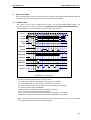
7.4.
USER’S MANUAL (Rev. 2.01)
I/O DETAILS
A memory access controller, DUART/LPT, timer, and interrupt controller are among the I/O devices
mapped in the memory space. The various I/O allocations are as follows.
PIC
reserved
TIMWR
ECP
PRN
SCC1
SCC0
PIC
Virtual address
0xBEFF FFFF
reserved
+0x00 7000
+0x00 6000
+0x00 5000
+0x00 4000
+0x00 3000
+0x00 2000
+0x00 1000
+0x00 0000
0xBB00 0000
SRAMC
DRAMC
+0x00 6000
+0x00 5000
SDRAMINIT +0x00 4000
reserved +0x00 3000
7Seg
+0x00 2000
SW2
+0x00 1000
SW1
+0x00 0000
DMAC
0xBA00 0000
0xB900 0000
0xB800 0000
I/O Map
Since kernel non-cached space access is assumed for these I/Os, logical addresses are used in the
following explanation.
7.4.1.
SRAM Controller (SRAMC B800-6000[Read/Write])
The SWAIT register performs wait control for the SRAM space. 0 to 3 waits can be set for the read
cycle using this register. The register allocation is as follows.
Data bus
Logical address
B800-6000H
Register
SRAMC SWAIT
D3
D2
D1
D0
0
0
SWAIT1
SWAIT0
SWAIT[1..0]: Sets the number of waits during SRAM read.
SWAIT
Number of SRAM read waits
1
0
0
0
0
0
1
1
1
0
2
1
1
3
Recommended value
(Reset value)
15
RTE-VR5432-CB
7.4.2.
USER’S MANUAL (Rev. 2.01)
DRAM Controller (DRAMC B800-5000[Read/Write])
DRAMC sets the access conditions. The register allocation is as follows.
Data bus
Logical address
B800-5000H
Register
D3
D2
D1
D0
DRAMC RCD
0
0
RCD1
RCD0
-5010H
DRAMC RP
0
0
RP1
RP0
-5020H
DRAMC RC
0
RC2
RC1
RC0
-5030H
DRAMC RRC
0
RRC2
RRC1
RRC0
-5040H
DRAMC RAS
0
RAS2
RAS1
RAS0
-5050H
DRAMC LAT
0
0
LAT1
LAT0
-5060H
DRAMC RSC
0
0
RSC1
RSC0
-5070H
DRAMC AP
0
0
0
AP
RCD[1..0]: Sets SDRAM parameter tRCD (Delay ACT to read/write).
RCD
tRCD
Remark
1
0
0
0
0
1
--
1
0
2 SYSCLK
Recommended value
1
1
3 SYSCLK
(Reset value)
--
Memo Use the recommended value. The operation is not guaranteed if a value other than the
recommended value is used.
RP[1..0]: Sets SDRAM parameter tRP (PRE to ACT/REF).
RP
tRP
Remark
1
0
0
0
--
0
1
--
1
0
2 SYSCLK
Recommended value
1
1
3 SYSCLK
(Reset value)
Memo Use the recommended value. The operation is not guaranteed if a value other than the
recommended value is used.
16
RTE-VR5432-CB
USER’S MANUAL (Rev. 2.01)
RC[2..0]: Sets SDRAM parameter tRC (ACT to REF/ACT).
RC
tRC
2
1
0
0
0
0
--
0
0
1
--
0
1
0
--
0
1
1
--
1
0
0
--
1
0
1
5 SYSCLK
1
1
0
6 SYSCLK
1
1
1
7 SYSCLK
Remark
Recommended value
(Reset value)
Memo Use the recommended value. The operation is not guaranteed if a value other than the
recommended value is used.
RRC[2..0]: Sets SDRAM parameter tRRC (REF to REF/ACT).
RRC
tRRC
Remark
2
1
0
0
0
0
--
0
0
1
--
0
1
0
--
0
1
1
--
1
0
0
--
1
0
1
--
1
1
0
6 SYSCLK
Recommended value
1
1
1
7 SYSCLK
(Reset value)
Memo Use the recommended value. The operation is not guaranteed if a value other than the
recommended value is used.
RAS[2..0]: Sets SDRAM parameter tRC (ACT to PRE).
RAS
tRAS
2
1
0
0
0
0
--
0
0
1
--
0
1
0
--
0
1
1
--
1
0
0
4SYSCLK
1
0
1
--
1
1
0
--
1
1
1
7 SYSCLK
Remark
Recommended value
(Reset value)
Memo Use the recommended value. The operation is not guaranteed if a value other than the
recommended value is used.
17
RTE-VR5432-CB
USER’S MANUAL (Rev. 2.01)
LAT[1..0]: Sets SDRAM parameter tLAT (/CAS latency).
LAT
tLAT
Remark
1
0
0
0
0
1
--
1
0
2 SYSCLK
Recommended value
1
1
3 SYSCLK
(Reset value)
--
Memo Use the recommended value. The operation is not guaranteed if a value other than the
recommended value is used.
RSC[1..0]: Sets SDRAM parameter tRSC (Mode Register Set Cycle Time).
RSC
tRSC
Remark
1
0
0
0
0
1
--
1
0
2 SYSCLK
Recommended value
1
1
3 SYSCLK
(Reset value)
--
Memo Use the recommended value. The operation is not guaranteed if a value other than the
recommended value is used.
AP: Sets whether to use the SDRAM automatic precharge function.
AP
Automatic precharge
0
Use
1
Don’t use
Remark
Reset value
7.4.3.
DRAM Initialization Port (DRAM_INIT B800-4000H[Write Only])
SDRAM is initialized based on the DRAMC setting value. Data is don’t care. The Mode Register Set
command of SDRAM is issued when output is performed.
This port is used to write the parameters set for the ports to SDRAM. After setting all the parameters to
the ports, output them to this port as the last step.
7.4.4.
SW1 Read Port (SW1 B800-0000H [Read Only])
This port is used to read the status of SW1. The table below indicates the data format.
Physical address
B800000H
input
Data bus
D7
D6
D5
D4
D3
D2
D1
D0
SW1
-8
SW1
-7
SW1
-6
SW1
-5
SW1
-4
SW1
-3
SW1
-2
SW1
-1
Setting
0 = ON
1 = OFF
SW1-1 corresponds to switch 1 of SW1, while SW1-8 corresponds to switch 8 of SW1. When a bit of
the corresponding switch is set to ON, 0 is read. When it is set to OFF, 1 is read. SW1 is used to set
the operation of the monitor. For how to set this switch, see 11.1.2 SW1 Setting and 12.1.1 SW1
Setting.
18
RTE-VR5432-CB
7.4.5.
USER’S MANUAL (Rev. 2.01)
SW2 Read Port (SW2 B800-1000H [Read Only])
This port is used to read the status of SW2. The data format of this port is shown in the table below.
Physical address
Data bus
Setting
D7
D6
D5
D4
D3
D2
D1
D0
B801000H
SW2
SW2
SW2
SW2
SW2
SW2
SW2
SW2
0 = ON
input
-8
-7
-6
-5
-4
-3
-2
-1
1 = OFF
SW2-1 corresponds to bit 1 of SW2, and SW2-8 corresponds to bit 8 of SW2. When a bit of the
corresponding switch is set to ON, 0 is read; when it is set to OFF, 1 is read. SW2 is used to switch the
hardware operation. For the function of each switch, see 5.4 SWITCH2 (SW2).
7.4.6.
7-Segment LED Display Data Output Port (7SEG-LED B800-2000 [Write Only])
This port sets the data to be displayed on the four 7-segment LED. The table below indicates the data
format. When a bit is set to 0, the corresponding segment is turned on.
Data
Logical address
Setting
D7..31 D6..30 D5..29 D4..28 D3..27 D2..26 D1..25 D0..24
B800-2000H
output
LED1
-DP
LED1
-G
LED1
-F
LED1
-E
LED1
-D
LED1
-C
LED1
-B
LED1
-A
B800-2001H
LED2
LED2
LED2
LED2
LED2
LED2
LED2
LED2
output
-DP
-G
-F
-E
-D
-C
-B
-A
B800-2002H
LED3
LED3
LED3
LED3
LED3
LED3
LED3
LED3
output
-DP
-G
-F
-E
-D
-C
-B
-A
B800-2003H
output
LED4
-DP
LED4
-G
LED4
-F
LED4
-E
LED4
-D
LED4
-C
LED4
-B
LED4
-A
0 = Turned on
1 = Turned off
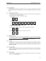
The figure below illustrates the correspondence between the bits and the segments of the
7-segment LED.
A
F
B
G
C
E
D
DP
19
RTE-VR5432-CB
7.4.7.
USER’S MANUAL (Rev. 2.01)
Serial/parallel I/O (SCC0/1 LPT B900-1000 to B900-4000[Read/Write])
The TL16PIR552 (dual UART with 1284 parallel port) made by Texas Instruments is used as the
UART/printer. The TL16PIR552 provides two UART channels and an IEEE1284-compliant bidirectional printer port (1 channel). The UART send/receive block features a 16-character FIFO buffer,
and a function to automatically control the RTS/CTS flow is provided, which reduces overrun errors
with a minimum of interrupts.
The TL16PIR552 registers are allocated as indicated in the table. For the functions of the registers,
see the TL16PIR552 manual. (The TL16PIR552 manual can be obtained in the TI&ME corner in the
homepage of Texas Instruments (http://www.ti.com/).
Address
Function
Read
Write
B900-1000
UART-CH#0
RBR/DLL
THR/DLL
IER/DLM
IER/DLM
B900-1020
IIR
FCR
B900-1030
LCR
LCR
B900-1040
MCR
MCR
B900-1050
LSR
LSR
B900-1060
MSR
MSR
B900-1070
SCR
SCR
RBR/DLL
THR/DLL
B900-2010
IER/DLM
IER/DLM
B900-2020
IIR
FCR
B900-1010
B900-2000
UART-CH#1
B900-2030
LCR
LCR
B900-2040
MCR
MCR
B900-2050
LSR
LSR
B900-2060
MSR
MSR
B900-2070
B900-3000
PRINTER(PPCS-)
SCR
SCR
DATA
DATA/ECPAFIFO
B900-3010
DSR
-----
B900-3020
DCR
DCR
B900-3030
EPPADDR
EPPADDR
B900-3040 to B900-3070
B900-4000
PRINTER(ECPCS-)
EPPDATA
EPPDATA
PPDATAFIFO/
TESTFIFO/CNFGA
PPDATAFIFO/
TESTFIFO
B900-4010
CNFGB
-----
B900-4020
ECR
ECR
TL16PIR552 Register Allocation
A 16-MHz clock is connected to the XIN input of the TL16PIR552.
The UART-CH#0, UART-CH#1, and PRINTER interrupts can be connected to CPU interrupts via PIC.
UART-CH#0, UART-CH#1, and PRINTER are connected to the JSIO1 connector, JSIO2 connector,
and JPRT on the rear panel, respectively. Moreover, UART-CH#0 is used when using a debugger for
serial transmission, and INT0 is used via PIC as the interrupt at this time.
The TL16PIR552 is reset by system reset.
Caution Do not change the contents of UART-CH#0 when using the monitor.
20
RTE-VR5432-CB
7.4.8.
USER’S MANUAL (Rev. 2.01)
Timer (Timer B900-5000[Read/Write])
NEC’s µPD71054 is used as the timer. The µPD71054 is compatible with Intel’s i8254, and is provided
with three timer counters. Various types of control can be performed using these timers.
The µPD71054 registers are allocated as shown in the table below.
Logical address
Register
Complement
B900-5000
PCNT0
Timer 0
B900-5010
PCNT1
Timer 1
B900-5020
PCNT2
Timer 2
B900-5030
PCNTL
Control
For the functions of the registers, see the manual of the µPD71054.
The timer is used as follows.
Timer
Clock
Mode
Application
0
2MHz
2
Timer interrupt 0
Used for monitor
1
2MHz
2
Timer interrupt 1
Can be used by user
2
2MHz
2
DRAM refresh
Caution Do not change the contents of timer 0 when using the monitor.
21
RTE-VR5432-CB
7.4.9.
USER’S MANUAL (Rev. 2.01)
Interrupt Controller (PIC B900-0000[Read/Write])
PIC performs interrupt control. The register allocation is as follows.
Data bus
Logical address
Register
D7
D6
D5
D4
D3
D2
D1
D0
B900-0000
PIC
INT0M
IM07 IM06 IM05 IM04 IM03 IM02 IM01 IM00
B900-0010
PIC
INT1M
IM17 IM16 IM15 IM14 IM13 IM12 IM11 IM10
B900-0020
PIC
INTR
B900-0030
PIC
INTEN
IR7
IR6
IR5
IR4
IR3
IR2
0
0
0
0
0
0
IR1
IR0
INT1 INT0
EN
EN
The INT0M and INT1M registers mask interrupts input to INT0 and INT1, respectively. They are
enabled when the IM0x and IM1x bits are “1,” and when several bits have been selected, interrupts
become active through ORing.
The INTR register is the interrupt status, and “1” is read when there is an interrupt request, regardless
of the mask status. Write “1” to the bit corresponding to this register to clear an edge interrupt request.
The interrupt sources allocated to the IM0[0..7], IM1[0..7], and IR[0..7] bits are as follows.
IM0,IM1,IR
Interrupt source
Request level
0
Timer 0 (Mode 2)
Edge (rising)
1
Serial 0
Level (high)
2
GBUS-INT0-
Level (low)
3
BUS ERROR
Level (low)
4
Timer 1 (Mode 2)
Edge (rising)
5
Serial 1
Level (high)
6
Parallel (printer)
Edge (rising)
7
DMAC INTREQ-
Level (low)
The INTEN register enables/disables interrupts to INT0, INT1.
INTEN0: Controls INT0. INT0 can be disabled by hardware with this bit. At this time, the status of the
INT0 pin changes to high level.
INTEN0
INT0
0
Disable
1
Enable
(Reset value)
INTEN1: Controls INT1. INT0 can be disabled by hardware with this bit. At this time, the status of the
INT1 pin changes to high level.
INTEN1
INT1
0
Disable
1
Enable
(Reset value)
Caution Do not change INT0-related contents when using the monitor.
22
RTE-VR5432-CB
USER’S MANUAL (Rev. 2.01)
7.4.10. DMA Controller
This controller is used to perform DMA transfer between GBUS resources in response to DMA
requests from GBUS. A total of 4 DMA controller channels are provided.
DMA transfer is normally performed in 2 cycles (read cycle and write cycle). Burst cycles are not
supported.
7.4.10.1.
7.4.10.2.
7.4.10.3.
7.4.10.4.
DMA channel 0 control port (DMACNT0 BA00-0000[Read/Write])
DMA channel 1 control port (DMACNT1 BA00-0080[Read/Write])
DMA channel 2 control port (DMACNT2 BA00-0100[Read/Write])
DMA channel 3 control port (DMACNT3 BA00-0180[Read/Write])
Bit
Signal name
RST
0
DMA_EN*1
0
1
TC*2
0
Function
0: Stop DMA
1: Execute DMA
0: DMA transfer not completed
1: DMA transfer completed
*3
2
DMA_SINGLE
3
SOFT_DREQ*4
x
4
DATA_SIZE[0] *5
x
5
DATA_SIZE[1] *5
x
6
Not used
x
7
Not used
x
8
DST_CD[0] *6
x
9
DST_CD[1] *6
x
10
Not used
x
11
Not used
x
0: Continuously use GBUS.
1: Release GBUS once after every transfer
0: Perform DMA transfer according to the hardware DMA request line.
1: Perform DMA transfer even if the hardware DMA request line is inactive.
Set size of data to be transferred with DATA_SIZE[1:0].
Set transfer destination address increase/decrease with DST_CD[1:0].
x
*6
12
SRC_CD[0]
13
SRC_CD[1] *6
x
14
Not used
x
15
Not used
x
16
DST_CS[0] *7
x
Specify the GBUS chip select space of the transfer destination address with
17
DST_CS[1] *7
x
DST_CS[1:0].
18
DST_CS[2] *7
x
19
Not used
x
20
SRC_CS[0] *7
x
Specify the GBUS chip select space of the transfer destination address with
21
SRC_CS[1] *7
x
SRC_CS[1:0].
*7
x
22
SRC_CS[2]
23
Not used
x
24
Not used
x
25
Not used
x
26
Not used
x
27
Not used
x
28
Not used
x
29
Not used
x
30
Not used
x
31
Not used
x
Set transfer destination address increase/decrease with SRC_CD[1:0].
x
23
RTE-VR5432-CB
USER’S MANUAL (Rev. 2.01)
<<Cautions>>
1. Set “1” to DMA_EN after completing the settings of the other bits. Do not change DMA_EN from “0”
to “1” while manipulating other bits.
Do not overwrite other bits in the DMA controller when DMA_EN is “1.” The operation is not
guaranteed if other bits are overwritten at this time.
2. TC becomes “1” after the number of bytes set in the Byte Count register has been transferred.
Write “1” to this bit to clear TC.
Prior to clearing TC, write “0” to DMA_EN. If TC is cleared while DMA_EN is “1,” DMA starts again
the instant it is cleared.
3. When DMA_SINGLE is set to “1,” the DMA controller gives up the GBUS mastership every time
one DMA transfer is completed, enabling the CPU to use the GBUS. When DMA_SINGLE is set to
“0,” DMA is continued while the DMA controller retains the GBUS mastership, and the CPU cannot
acquire the GBUS mastership until DMA transfer ends. For details, see 7.4.10.19 Single transfer
and non-single transfer.
4. When SOFT_DREQ is set to “1,” DMA transfer is performed without the need for hardware DMA
requests. However, even if SOFT_DREQ is “1,” the DMAAK signal of the GBUS becomes active
during the DMA cycle.
5. The DATA_SIZE[1:0] settings are as follows.
[0,0]: 8-bit transfer
[0,1]: 16-bit transfer
[1,0]: 32-bit transfer
[1,1]: Setting prohibited
6. The DST_CD[1:0] and SRC_CD[1:0] settings are as follows. The transfer address
increment/decrement unit is determined by the DATA_SIZE[1:0] setting.
[0,0]: Fixed
[0,1]: Increment
[1,0]: Decrement
[1,1]: Setting prohibited
7. The DST_CS[2:0] and SRC_CS[2:0] settings are as follows.
[0,0,0]: GCS0 space
[0,0,1]: GCS1 space
[0,1,0]: GCS2 space
[0,1,1]: GCS3 space
[1,0,0]: GCS4 space
[1,0,1]: GCS5 space
[1,1,0]: GCS6 space
7.4.10.5.
7.4.10.6.
7.4.10.7.
7.4.10.8.
DMA channel 0 transfer origin address port (DMASRCADDR0 BA00-0010[Read/Write])
DMA channel 1 transfer origin address port (DMASRCADDR1 BA00-0090[Read/Write])
DMA channel 2 transfer origin address port (DMASRCADDR2 BA00-0110[Read/Write])
DMA channel 3 transfer origin address port (DMASRCADDR3 BA00-0190[Read/Write])
These ports are used to set DMA transfer origin addresses. 24 bits from A0 to A23 are effective for the
address. Transfer addresses must be aligned to the data size specified in DATA_SIZE[1:0] set to the
DMA control port of each channel. The operation in case the set addresses are not aligned is undefined.
The contents of the address to be used for DMA transfer can be read from these ports during DMA
transfer or upon DMA transfer end.
24
RTE-VR5432-CB
7.4.10.9.
7.4.10.10.
7.4.10.11.
7.4.10.12.
USER’S MANUAL (Rev. 2.01)
DMA channel 0 transfer destination address port (DMADSTADDR0 BA00-0020[Read/Write])
DMA channel 1 transfer destination address port (DMADSTADDR1 BA00-00A0[Read/Write])
DMA channel 2 transfer destination address port (DMADSTADDR2 BA00-0120[Read/Write])
DMA channel 3 transfer destination address port (DMADSTADDR3 BA00-01A0[Read/Write])
These ports are used to set DMA transfer destination addresses. 24 bits from A0 to A23 are effective for
the address. Transfer addresses must be aligned to the data size specified in DATA_SIZE[1:0] set to the
DMA control port of each channel. The operation in case the set addresses are not aligned is undefined.
The contents of the address to be used for DMA transfer can be read from these ports during DMA
transfer or upon DMA transfer end.
7.4.10.13.
7.4.10.14.
7.4.10.15.
7.4.10.16.
DMA channel 0 byte count port (DMABYTECNT0 BA00-0030[Read/Write])
DMA channel 1 byte count port (DMABYTECNT1 BA00-00B0[Read/Write])
DMA channel 2 byte count port (DMABYTECNT2 BA00-0130[Read/Write])
DMA channel 3 byte count port (DMABYTECNT3 BA00-01B0[Read/Write])
These ports are used to set the number of bytes to be DMA transferred - 1. 24 bits of data from Bit 0
to Bit 24 are effective. The DMA controller decrements the contents of this port by 1, 2, or 4 according to
the data size specified in DATA_SIZE[1:0] set for the DMA control port of each channel, every time one
DMA transfer ends. DMA ends when result carry for this decrementing operation occurs (TC becomes
“1.”)
The current byte counter value can be read during DMA transfer or upon DMA transfer end.
7.4.10.17. DMA interrupt control port (DMAINTCNT BA00-0200[Read/Write])
Bit
Signal name
RST
Function
0
INT_EN[0]
0
0: Don’t request interrupt when TC bit of channel 0 is “1.”
0: Request interrupt when TC bit of channel 0 is “1.”
1
INT_EN[1]
0
0: Don’t request interrupt when TC bit of channel 1 is “1.”
0: Request interrupt when TC bit of channel 1 is “1.”
2
INT_EN[3]
0
0: Don’t request interrupt when TC bit of channel 2 is “1.”
0: Request interrupt when TC bit of channel 2 is “1.”
3
INT_EN[4]
0
0: Don’t request interrupt when TC bit of channel 3 is “1.”
0: Request interrupt when TC bit of channel 3 is “1.”
4
TC[0] *1
0
Read contents of TC bit of channel 0.
5
TC[1] *1
0
Read contents of TC bit of channel 1.
6
TC[2] *1
0
Read contents of TC bit of channel 2.
7
TC[3] *1
0
Read contents of TC bit of channel 3.
<<Caution>>
For TC[3:0], the contents of Bit 1 of the DMA control port can be read as is. This bit enables
judgment of which channel has issued an interrupt request.
TC[3:0] of this port is read-only, and when TC is cleared, TC of the control port of each channel
must be manipulated.
7.4.10.18. Priority
Channel 0 has the highest priority, and channel 3 has the lowest priority. If several DMA requests are
contending, which channel DMA transfer is to be performed is judged based on the status of the DMA
request immediately before the start of the bus cycle following acquisition of the GBUS mastership.
25
RTE-VR5432-CB
USER’S MANUAL (Rev. 2.01)
7.4.10.19. Single transfer and non-single transfer
The setting made in DMA_SINGLE of the DMA control port determines whether the GBUS mastership
is relinquished following the end of DMA transfer of 1 cycle for each channel. The setting made in
DMA_SINGLE of each channel determines the status following the DMA transfer cycle of the
corresponding channel.
When DMA_SINGLE is set to “1,” the DMA controller relinquishes the GBUS mastership every time
one DMA transfer has ended, giving the CPU the opportunity to use the GBUS. If this is followed by an
active DMA request, the DMA controller again requests mastership of the GBUS.
When DMA_SINGLE of the DMA control port is set to “0,” the DMA controller does not relinquish the
GBUS mastership in the case of an active DMA request (or if SOFT_DREQ is “1”) even if transfer ends,
and DMA transfer is continued. However, since arbitration of priority between channels is performed,
DMA transfer is not necessarily performed for the same channel.
7.4.10.20. DMA request sample timing during non-single transfer
Whether or not to perform the DMA cycle during non-single transfer depends on the DMA request
status at the timing (GREADY = Low, GWAITI = High) when the write cycle to the transfer destination
becomes ready. If this timing corresponds to when a DMA request is active, the DMA controller keeps
the GBUS mastership and DMA transfer is continued.
26
RTE-VR5432-CB
8.
8.1.
USER’S MANUAL (Rev. 2.01)
BUS CYCLE TIMING
In the RTE-VR5432-CB, access is performed from the SYSAD via the bridge for SRAM, DRAM, ROM, and
I/O devices. The basic control timing for each access cycle is described below.
SRAM ACCESS
The number of wait cycles for SDRAM read access is set with the SRAMC-SWAIT register. The
selection range is 0 to 3 wait cycles. (See 7.4.1 SRAM Controller (SRAMC B800-6000[Read/Write].)
The following figure shows an example of burst read with 2 wait cycles set.
0
1
2
3
4
5
6
7
8
9
10 11 12 13 14 15 16 17 18 19
SYSCLK
SYSAD
SYSCMD
A
EOD
READ
PVALIDEOKPMASTEREVALIDSRAM-ADDR
A
SRAM-DATA
SRAM CSSRAM ADSPSRAM ADSCSRAM ADV-
Ws Ws
Ws Ws
Ws Ws
Ws Ws
SRAM G-
Read (burst 4 word)
SRAM Read Cycle (SWAIT[]=2)
The status is described below following the clock number.
0 to 1: The CPU’s external read cycle starts. Normally, EOK- is inactive.
2 to 3: The SRAM read cycle is determined and EOK- becomes active.
3 to 4: The number of wait cycles set with SWAIT (in this example, 2) is inserted.
5: A read command is issued to PBSRAM.
7: Data is output from PBSRAM. EVALID- is returned accordingly.
8 to 16: Cycles are repeated until the last data (EOD).
(6 to 8): The number of wait cycles set with SWAIT (in this example, 2) is inserted.
SRAM ADV- is made active, and the internal address of PBSRAM is incremented.
Note In the case of 8-word burst data, the SRAM ADSP signal is made active at clock 16, an address
is provided from external, and burst processing continues.
27
RTE-VR5432-CB
USER’S MANUAL (Rev. 2.01)
The SRAM write cycle follows the CPU’s output data rate (DDDD or DxxDxxDxxDxx). In the case of
SRAM, EOK- is returned 2 clocks after address determination and the cycle is started. The following
figure shows an example of the burst cycle of data rate DxxDxxDxxDxx.
0
1
2
3
4
5
6
7
8
9
10 11 12 13 14 15 16 17 18
SYSCLK
SYSAD
SYSCMD
A
READ
EOD
PVALIDEOKPMASTEREVALIDSRAM-ADDR
A
SRAM-DATA
SRAM CSSRAM ADSPSRAM ADSCSRAM ADVSRAM W-
Write (burst 4 word)
SRAM Write Cycle (DxxDxxDxxDxx)
The status is described below following the clock number.
0 to 1: The CPU’s external write cycle starts. Normally, EOK- is inactive.
2 to 3: The SRAM write cycle is determined and EOK- becomes active.
4: The first data output is performed. At this time, the data is directly latched to PBSRAM and the write
operation starts. The address is latched beforehand and provided simultaneously at this time.
5 to 13: The write operation is repeated. The address counter in PBSRAM is incremented for the
second and subsequent write cycles. The timing for SRAM ADV- and SRAM W is adjusted to the data
rate. (When the data rate is DDDD, the active status occurs continuously.)
28
RTE-VR5432-CB
8.2
USER’S MANUAL (Rev. 2.01)
DRAM ACCESS
DRAM controller settings are required for DRAM. (See 7.4.2 DRAM Controller (DRAMC B8005000[Read/Write].) In the following example, all the settings correspond to the recommended values.
The DRAM read cycle when PAGE = 0 (auto precharge ON) is shown below. However, this corresponds
to the start of the cycle, if refresh and precharge do not overlap. If they overlap, the end of these cycles
is waited for.
0
1
2
3
4
5
6
7
8
9
10 11 12 13 14 15 16 17 18 19
SYSCLK
SYSAD
SYSCMD
A
READ
EOD
PVALIDEOKPMASTEREVALIDDRAM-ADDR
Acol
Araw
DRAM-DATA
DRAM CSDRAM RASDRAM CASDRAM WEDRAM CKE
Read (burst 8 word)
DRAM Read Cycle
The status is described below following the clock number.
0 to 1: The CPU’s external read cycle starts. Normally, EOK- is inactive.
2 to 3: Access to DRAM is determined, EOK- becomes active, and at clock 3, an active command is
issued for SDRAM. The row address is given to DRAM ADDR at this time.
4 to 5: tRCD is waited for and a read command is issued to SDRAM at clock 5. At this time, the column
address is given to DRAM ADDR.
7: The first read data is determined. EVALID- is made active, and this data is directly read to the CPU.
8 to 14: Data is read from SDRAM in continuous bursts. During this time, EVALID- to the CPU is made
active. A burst stop command is issued during clock 13, and a precharge command is issued during
clock 14.
Note If AP = 1 (auto precharge OFF), no precharge command is issued at clock 14.
29
RTE-VR5432-CB
USER’S MANUAL (Rev. 2.01)
The DRAM write cycle follows the CPU’s output data rate (DDDD or DxxDxxDxxDxx). In the case of
DRAM, an active command is issued 3 clocks after the address is determined, and 1 clock later EOK- is
returned to start the cycle. The following figure shows an example of the burst cycle with data rate
DxxDxxDxxDxx.
0
1
2
3
4
5
6
7
8
9
10 11 12 13 14 15 16 17 18 19
SYSCLK
A
SYSAD
SYSCMD
WRITE
EOD
PVALIDEOKPMASTEREVALIDDRAM-ADDR
Acol
Araw
DRAM-DATA
DRAM CSDRAM RASDRAM CASDRAM WEDRAM CKE
Write (burst 4 word)
DRAM Write Cycle (DxxDxxDxxDxx)
The status is described below following the clock number.
0 to 1: The CPU’s external write cycle starts. Normally, EOK- is inactive.
2 to 3: The DRAM write cycle is determined, and an active command is issued for SDRAM at clock 3.
At this time, the row address is given to DRAM ADDR.
4 to 6: EOK- becomes active 1 clock after the active command, and 2 clocks after EOK-, the CPU’s
external write cycle starts.
7: The first data output is performed. A write command is issued for SDRAM so that this data can be
written directly. The column address is given to DRAM ADDR at this time.
8 to 16: The write operation is repeated. From the second and subsequent writes, the timing is taken
from DRAM_CKE to synchronize with the data rate.
17: The burst stop command is issued to SDRAM.
18. The precharge command is issued to SDRAM.
Note When AP = 1 (auto precharge OFF), no precharge command is issued at clock 18.
30
RTE-VR5432-CB
USER’S MANUAL (Rev. 2.01)
When AP = 1 (auto precharge OFF), during the interval until precharge is issued, the lower address in
SDRAM is temporarily held. If access is performed to the same lower address space in this status (hit),
the active command is skipped, so that SDRAM access starts two clock cycles earlier for both the read
cycle and the write cycle. However, in the case of non-match (miss hit), precharge must be performed
before the target address, so that the overhead increases.
SDRAM refresh uses the CBR (auto) refresh command, and refresh is performed approximately every
15 µs through the setting of Timer 2.
31
RTE-VR5432-CB
8.3.
USER’S MANUAL (Rev. 2.01)
LOCAL BUS ACCESS
The local bus is a sync bus that has a data width of 32 bits and operates at 1/2 SYSCLK.
The following figure shows the read cycle on the local bus.
0
1
2
3
4
5
6
7
8
9
10 11 12 13 14 15 16 17 18
SYSCLK
SYSAD
SYSCMD
A
READ
EOD
PVALIDEOKPMASTEREVALIDLBUS CLK
LBUS ADDR
A
LBUS DATA
LBUS RDLBUS RDY-
Read (Single)
LBUS Read Cycle
The status is described below following the clock number.
0 to 1: The CPU’s external read cycle starts. Normally, EOK- is inactive.
2 to 3: The read cycle to the LBUS is determined, and EOK- becomes active.
6: The read cycle to the LBUS starts.
8 to 9: The clocks in this interval differ according to the accessed resource.
13 to 15: The fact that data has been prepared on the LBUS is indicated by the fact that status
becomes active at LBUS RDY.
Data from LBUS is output to SYSAD in synchronization with SYSCLK. Following LBUS RDY, EVALIDis returned to the CPU at clock 15 and the bus operation ends.
32
RTE-VR5432-CB
USER’S MANUAL (Rev. 2.01)
The following figure shows the write cycle on the local bus.
0
1
2
3
4
5
6
7
8
9
10 11 12 13 14 15 16 17 18
SYSCLK
SYSAD
SYSCMD
A
WRITE
EOD
PVALIDEOKPMASTEREVALIDLBUS CLK
LBUS ADDR
A
LBUS DATA
LBUS WRLBUS RDY-
Write (Single)
LBUS Write Cycle
The status is described below following the clock number.
0 to 1: The CPU’s external write cycle starts. Normally, EOK- is inactive.
2 to 3: The write cycle of the LBUS is determined and EOK- becomes active.
4: Data output is performed. The LBUS controller latches the data at this time. The CPU cycle ends at
this point, but the write cycle actually continues.
6. The write cycle to the LBUS starts.
8 to 9: The clocks in this interval differ according to the accessed resource.
13 to 14: The LBUS write cycle ends when LBUS RDY becomes active.
33
RTE-VR5432-CB
8.4.
USER’S MANUAL (Rev. 2.01)
LIST OF REQUIRED CLOCKS
The following tables list the required number of clocks for memory access.
8.4.1.
SRAM Access
Cycle type
1st
2nd
3rd
4th
5th
6th
7th
8th
total
SingleRead
6+n
6+n
SingleWrite
5
5
8 BurstRead
6+n
1+n
1+n
1+n
4 BurstWrite
5
1+n
1+n
1+n
1+n
1+n
1+n
1+n
Remark
SWAIT[] = 0
DDDD
13 + 8*n
SWAIT[] = 0
8 + 3 *n
DDDD
Note In the read cycle, n = SWAIT[]. In the write cycle, n = 2 for data rate DxxDxx.
8.4.2.
SDRAM Access
Cycle type
1st
2nd
3rd
4th
SingleRead
8
SingleWrite
8
8 BurstRead
8
1
1
1
4 BurstWrite
8
1+n
1+n
1+n
Notes
5th
6th
7th
8th
total
Remark
DDDD
1
1
1
1
15
11 + 3 *n
SWAIT[] = 0
DDDD
1. In the write cycle, n = 2 for data rate DxxDxx.
2. When auto precharge is ON, the precharge time following the last cycle is added, but there
is no penalty if there are two or more idle cycle clocks by the start of the next cycle from the
last cycle.
3. If the auto precharge is OFF, the first cycle of the cycles during which the row address has
hit is shorted by 2 clocks. Inversely, in the case of no hit, a precharge cycle is inserted
immediately before the 1st cycle, so that 2 clocks are added.
34
RTE-VR5432-CB
9.
9.1
USER’S MANUAL (Rev. 2.01)
ROM PROGRAMMING
Refer to the following section when preparing a program to be placed in ROM on the board.
INITIALIZATION
In the reset processing routine, following processor register initialization, set Timer 2 for the memory
access controller and DRAM refresh.
The following describes board-specific items. For other details, see the manual for the CPU.
<Initialization of Processor Contents>
Config Reg
⋅⋅⋅ SW2-4 = OFF >>EP = 0x6(DxxDxx)
SW2-4= ON >>EP = 0x0(DDDD)
<SRAM Wait Initialization>
[0xB8006000+ offset].b <= 0
⋅⋅⋅ SRAM Wait >> 0 waits
<SDRAM Controller Initialization>
[0xB8005000+ offset].b <= 2
⋅⋅⋅ SDRAM tRCD
>> 2 clocks
[0xB8005010+ offset].b <= 2
⋅⋅⋅ SDRAM tRP
>> 2 clocks
[0xB8005020+ offset].b <= 5
⋅⋅⋅ SDRAM tRC
>> 5 clocks
[0xB8005030+ offset].b <= 6
⋅⋅⋅ SDRAM tRRC
>> 6 clocks
[0xB8005040+ offset].b <= 4
⋅⋅⋅ SDRAM tRAS
>> 4 clocks
[0xB8005050+ offset].b <= 2
⋅⋅⋅ SDRAM tLAT
>> 2 clocks
[0xB8005060+ offset].b <= 2
⋅⋅⋅ SDRAM tRSC
>> 2 clocks
[0xB8005070+ offset].b <= 1
⋅⋅⋅ SDRAM AP
>>Auto precharge: Off (arbitrary)
[0xB8004000+ offset].b <= 0
⋅⋅⋅ SDRAM Mode Reg Set
<Refresh Timer Initialization>
[0xB9005030+ offset].b <= 0xb4
⋅⋅⋅ Timer 2 Mode 2 (Set to approx. 15 µs cycle)
[0xB9005020+ offset].b <= 0x1f
⋅⋅⋅ Timer 2 lower count
[0xB9005020+ offset].b <= 0x00
⋅⋅⋅ Timer 2 higher count
Memo Offset in the case of doing byte access by Big Endian is 3.
9.2
ROM DATA ASSIGNMENT
The remote monitor ROM is configured as four banks. Normally, set SW3-3 to ON to use these four
ROM banks as a continuous ROM space.
Since byte row rearrangement is performed by hardware for this board when the big endian is selected,
write also big endian code as is with a ROM writer. (Previously, such code had to be written in 16-bit
units using higher/lower 8-bit swapping.)
Memo Even if a ROM emulator is used, disable the ROM banks (set SW3-3 to ON).
35
RTE-VR5432-CB
USER’S MANUAL (Rev. 2.01)
10. SPECIFIC GBUS SPECIFICATIONS
This chapter describes the usage status of the GBUS for the RTE-VR5432-CB. For general GBUS
specifications, see 14 APPENDIX C GBUS COMMON SPECIFICATIONS.
10.1
OVERVIEW
An overview of the GBUS signal usage status for the RTE-VR5432-CB is provided in the following table.
GBUS signal name
Function
See
GADDR[31:2]
Used as address lines. GADDR [26:31] are not connected.
GDATA[31:0]
Used as data lines. In a read cycle, the signal that is latched on the rising
edge of SYSCLK is supplied to the CPU.
GCS-[6:0]
Created by the board and output as chip select lines
GCLK
Connects SYSCLK divided by 2.
GRESETI-
Output the reset request generated by the board.
7.1
GRESETO-
OR with reset signal on board and connect to Cold Reset*.
7.1
GADS- , GREADY- ,
GBLAST- , GW/R-
Used as bus control signal.
GWAITI-
Use as bus control signal.
GBTERM-
Use as bus control signal.
GRD- , GWR-
RD- and WR- signal generated from the GBUS control signals are
connected.
GHOLD- , GHLDA-
Not connected.
GBREQ-
Not connected.
GDMARQ-[3:0]
Used as DMA request signal.
7.4.10
GDMAAK-[3:0]
Used as DMA acknowledge signal.
7.4.10
GINTO-[3:0]
Used as interrupt request signal.
7.2
GINTI-[1:0]
OUT0 and OUT1 of TIC (µPD71054) are connected to GINTI0- and GINTI1-.
GETC[7:0]
Not connected.
GAHI_EN-
Not connected.
GMOTHER_DETECT-
Use for ready generation in case of access to GBUS when not connected to
JGBUS.
GUSE_DIRECT_ACC-
Not connected.
GCLK_LOW-
High when SW2-8 (BGCLK LOW-) OFF, Low when ON.
GLOCK-[1:0]
Not connected.
10.3
5.4
36
RTE-VR5432-CB
10.2
USER’S MANUAL (Rev. 2.01)
BUS CYCLE
Connect the CPU clock divided by 2 as GCLK to the GBUS. Since GAHI_EN- is not connected,
GADDR[26:31] is unconnected.
Both single cycle and burst cycle are supported for GBUS access.
The Gxxx signal is the GBUS signal in the following waveforms.
The read cycle (single) is described in the following table. (For the burst cycle, see 14.6.2 Burst Cycle.)
0
1
2
3
4
5
6
7
8
9
10 11 12 13 14 15 16 17 18
SYSCLK
SYSAD
SYSCMD
A
READ
EOD
PVALIDEOKPMASTEREVALIDGBUS CLK
GADDR
A
GDATA
GADSGRDY-
Read (Single)
GBUS Read Cycle
37
RTE-VR5432-CB
USER’S MANUAL (Rev. 2.01)
The write cycle (single) is described in the following table. (For the burst cycle, see 14.6.2 Burst Cycle.)
0
1
2
3
4
5
6
7
8
9
10 11 12 13 14 15 16 17 18
SYSCLK
SYSAD
SYSCMD
A
READ
EOD
PVALIDEOKPMASTEREVALIDGBUS CLK
GADDR
A
GDATA
GADSGRDY-
Write (Single)
GBUS Write Cycle
10.3
CHIP SELECT
The following spaces are assigned for the GBUS chip selects.
GBUS signal
Logical address range
Physical address range
Remark (RTE-MB-A resources)
name
GCS0-
0xB0000000 to 0xB0FFFFFF
0x10000000 to 0x10FFFFFF
(MB-SRAM)
GCS1-
0xB1000000 to 0xB1FFFFFF
0x11000000 to 0x11FFFFFF
FBOOT=OFF (MB-FLASH)
0xBF000000 to 0xBFFFFFFF
0x1F000000 to 0x1FFFFFFF
FBOOT=ON (MB-FLASH)
GCS2-
0xB2000000 to 0xB2FFFFFF
0x12000000 to 0x12FFFFFF
(MB-Peri)
GCS3-
0xB3000000 to 0xB3FFFFFF
0x13000000 to 0x13FFFFFF
(MB-EXT-MEM)
GCS4-
0xB4000000 to 0xB4FFFFFF
0x14000000 to 0x14FFFFFF
(MB-EXT-IO)
GCS5-
0xB5000000 to 0xB5FFFFFF
0x15000000 to 0x15FFFFFF
(MB-PCI Bus)
GCS6-
0xB6000000 to 0xB6FFFFFF
0x16000000 to 0x16FFFFFF
(MB-PCI9080 Reg)
Uncached areas are described for the physical addresses. If access is performed as cached areas,
subtract 0x20000000. While it is possible to perform burst access for the resources of this board as
cached areas, use the I/O space and common memory space on an uncached basis.
38
RTE-VR5432-CB
USER’S MANUAL (Rev. 2.01)
11. APPENDIX A MULTI MONITOR
This chapter describes how to make the settings required to establish a connection between the Multi
monitor stored in ROM and the Multi debugger on the host. It also provides notes on the use of the Multi
monitor.
11.1. BOARD SETTING
11.1.1. RTE for Win 32 Installation
When the board is used with the Multi debugger, communication software called RTE for Win32 must
be installed in the PC. Refer to the RTE for Win32 Installation Manual (supplied with this product) for
installation and test methods.
11.1.2. SW1 Setting
SW1 is a switch for general-purpose input ports. For the Multi monitor in the factory-installed ROM,
SW1 is used as shown below. Be sure to use the correct setting.
SW1
1
2
Setting
ON
ON
115,200 baud
Baud rate
OFF
ON
38,400 baud
ON
OFF
19,200 baud
OFF
OFF
9,600 baud
(Factory-set)
Baud Rate Setting
SW1
3
4
Setting
ON
ON
Timer is not used.
Profiler period
OFF
ON
200 Hz
5 ms
ON
OFF
100 Hz
10 ms
OFF
OFF
60 Hz
16.67 ms
(Factory-set)
Profiler Period Setting
SW1
Setting
8
Debugger mode
ON
Monitor uses 7-segment LED
OFF
Normal use state
(Factory-set)
Debug Mode Setting
SW1-5 to SW1-7 are not used with the Multi monitor.
11.1.3. Connection of Board
Connect the board to the PC serially, by referring to 6 CONNECTION WITH THE HOST PC.
39
RTE-VR5432-CB
USER’S MANUAL (Rev. 2.01)
11.2. MULTI MONITOR
The ROM monitor for Multi can be executed in any one of four modes: 32-bit big endian, 32-bit little
endian, 64-bit big endian, and 64-bit little endian. The monitor operating mode depends on the SW3-7:8
settings.
11.2.1. 7-Segment LED on Startup
The 7-segment LED of the ROM monitor for Multi operates as follows when power is supplied to the
board (black indicates the segment that lights).
1) Check operation of 7-segment LED (See figure below.)
If SW1-8 is OFF:
If SW1-8 is ON:
2) Number counting by simple SRAM memory check
* Not executed if SW1-8 is OFF.
3) Connection wait status (The dot does not blink if the profiler timer is stopped.)
4) Connection status (The status of the dot is retained on connection.)
or
11.2.2. Monitor Work RAM
The ROM monitor uses the first 64 Kbytes (from the start address to 1000H) in the SRAM (uncached)
as work RAM (reserved). In other words, user programs are not allowed to use logical addresses
8000-0000H to 8000-FFFFH and A000-0000H to A000-FFFFH, nor their image area.
11.2.3. Interrupt
The INT0 interrupt is used for the monitor. The vector for this interrupt is BFC0-0380H of ROM by
bootstrap (BEV = 1) setting. Therefore, it is not possible to overwrite the vector. With the monitor, it is
possible to overwrite the vector by branching once to a substitute vector securing A000 to 0180H of
the SRAM (uncached).
11.2.4. _INIT_SP Setting
_INIT_SP (stack pointer initial value) is set to 4F7FF0H (immediately before monitor work RAM) by the
monitor. (_INIT_SP can be changed in the Multi environment.) The monitor uses a 32-byte stack area
set by the user program.
11.2.5. Timer Interrupt
If the timer interrupt is disabled, the profiler function of Multi cannot be used (for how to set the timer
interrupt, see 11.1.2 SW1 Setting).
40
RTE-VR5432-CB
USER’S MANUAL (Rev. 2.01)
11.2.6. Initializing Hardware
The ROM monitor performs initialization so that the resources on the board can be directly accessed.
11.2.7. Special Instruction
The monitor uses the following instruction for the single step, breakpoint, and system call functions.
BREAK instruction (0xxxxxxdh)
Do not use a code that may be interpreted as a break instruction in the user program.
11.3. RTE COMMANDS
When the monitor and MIDAS server (RTESERV) are connected by the Multi debugger, the TARGET
window is opened. The RTE commands can be issued in this window. The following table lists the RTE
commands.
Command
HELP, ?
Description
Displays help messages.
INIT
Initializes.
VER
Displays the version number.
CACHEFLUSH
Flushes the cache
SHOWTLB
Displays the contents of the TLB
IOREAD
Reads the I/O (size specification)
IOWRITE
Writes to the I/O (size specification)
RTE Commands
Some commands require parameters. All numeric parameters such as addresses and data are
assumed to be hexadecimal numbers. The following numeric representations are invalid:
0x1234 1234H
$1234
11.3.1. HELP(?)
<Format>
HELP [command-name]
Displays a list of RTE commands and their formats. A question mark (?) can also be used in place of
the character string HELP. If no command name is specified in the parameter part, the HELP
command lists all usable commands.
<Example> HELP INIT
Displays help messages for the INIT command.
11.3.2. INIT
<Format>
INIT
Initializes the RTE environment. Usually, this command should not be used.
11.3.3. VER
<Format>
VER
Displays the version number of the current RTE environment.
11.3.4
CACHEFLUSH
<Format>
CACHEFLUSH
Flushes the cache contents of the CPU.
41
RTE-VR5432-CB
USER’S MANUAL (Rev. 2.01)
11.3.5
SHOWTLB
<Format>
SHOWTLB
Displays in list form the TLB contents of the CPU.
11.3.6
IOREAD
<Format>
IOREAD [BYTE|SHORT|LONG] [address]
Reads the address memory of the specified size and displays this data. The size can be specified as
8, 16, and 32 bits with BYTE, SHORT, and LONG, respectively. This command is used for memory
mapped I/O access.
<Example>
11.3.7
IOREAD BYTE 0xBC000100
BC000100: 1A
IOWRITE
<Format>
OWRITE [BYTE|SHORT|LONG] [data] [address]
Writes data to the address memory of the specified size. The size can be specified as 8, 16, and 32
bits with BYTE, SHORT, and LONG, respectively. This command is used for memory mapped I/O
access.
<Example>
OWRITE SHORT 0x30F0 0xBC00F000
42
RTE-VR5432-CB
USER’S MANUAL (Rev. 2.01)
12. APPENDIX B PARTNER MONITOR
This chapter describes how to make the settings required to establish a connection between the
PARTNER monitor stored in ROM and the PARTNER on the host. It also provides notes on the use of the
PARTNER monitor.
12.1. BOARD SETTING
12.1.1. SW1 Setting
SW1 is a switch for general-purpose input ports. For the PARTNER monitor in the factory-installed
ROM, SW1 is used as shown below. Be sure to use the correct setting.
SW1
Setting
1
2
Baud rate
ON
ON
115,200 baud
OFF
ON
38,400 baud
ON
OFF
19,200 baud
OFF
OFF
9,600 baud
(Factory-set)
Baud Rate Setting
SW1
3
4
Setting
ON
ON
SW1
Setting
Timer
Always use this switch in this status.
8
Debugger mode
ON
Monitor uses 7-segment LED
OFF
Normal use state
(Factory-set)
Debug Mode Setting
SW1-5 to SW1-7 are not used with the PARTNER monitor.
12.1.2. Connection of Board
Connect the board to the PC serially, by referring to 6 CONNECT WITH THE HOST PC.
43
RTE-VR5432-CB
12.2
USER’S MANUAL (Rev. 2.01)
PARTNER MONITOR
The partner ROM monitor can be executed using one of two modes: 32-bit big endian or 32-bit little
endian. The monitor operation mode depends on the SW3-7:8 settings.
12.2.1. 7-Segment LED on Startup
The 7-segment LED of the ROM monitor for PARTNER operates as follows when power is supplied to
the board (black indicates the segment that lights).
1) Check operation of 7-segment LED (See figure below.)
If SW1-8 is OFF:
If SW1-8 is ON:
2) Number counting by simple RAM memory check
* Not executed if SW1-8 is OFF.
3) Connection wait status
4) Connection status
12.2.2. ROM Monitor Work RAM
The ROM monitor uses the first 64 Kbytes (from the start address to 10000H) in the SRAM as work
RAM (reserved). In other words, user programs are not allowed to use logical addresses 8000-0000H
to 8000-FFFFH and A000-0000H to A000-FFFFH, nor their image area.
12.2.3. Interrupt
The INT0 interrupt is used as the interrupt for monitor communication and forcible breaks (ESC button).
The vector for this interrupt is BFC0-0380H of ROM by bootstrap (BEV = 1) setting. Therefore, it is not
possible to overwrite the vector. With the monitor, it is possible to overwrite the vector by branching
once to a substitute vector securing A000 to 0180H of the SRAM (uncached).
12.2.4. INIT_SP Setting
The initial value of the monitor’s stack pointer is set to A003-FFF0H (highest in SRAM). This value can
be changed with the INIT_SP command defined in the partner’s configuration file. The monitor uses
the 32-byte stack area set with the user program.
12.2.5. Remote Connection
The connection with the debugger is of the serial type. Correctly set the SW1 communication speed
setting and the setting of the communication speed with the transmission channel with RPTSETUP.
44
RTE-VR5432-CB
USER’S MANUAL (Rev. 2.01)
12.2.6. Initializing Hardware
The ROM monitor performs initialization so that the resources on the board can be directly accessed.
12.2.7. Special Instruction
The monitor uses the following instruction for the single step, breakpoint, and system call functions.
BREAK instruction (0xxxxxxdh)
Do not use a code that may be interpreted as a break instruction in the user program.
45
RTE-VR5432-CB
USER’S MANUAL (Rev. 2.01)
13. APPENDIX C INTERRUPT PROGRAMMING
This appendix describes interrupt processing in user programs using the monitor.
13.1. INTERRUPT LIBRARY
Since, in the VR5432, a vector is assigned for general exception interrupts as a group and interrupts are
used even in the monitor, this vector is used in common. An interrupt library (attached sample program:
Intvect.c, IntHdr.s/mip) is provided.
This library hooks vectors and is table managed for every exception for exception processing routine
execution. The eight provided library functions are described below.
13.1.1. int InitlrqVect(void)
Performs interrupt vector hooking and table initialization. Upon normal end, 0 is returned, and in case
of an error, a negative error number is returned.
13.1.2. int TermlrqVect(void)
Returns an interrupt vector. Upon normal end, 0 is returned, and in case of an error, a negative error
number is returned.
13.1.3. int SetlrqVect(int no, int func)
Registers (casts with int type) the function func to the interrupt processing table specified by argument
No. An item defined as a macro in the VECT_IPn format in the Intvect.h file is used.
When 0 is specified for func, the previously set processing routine becomes invalid. Upon normal end,
0 is returned, and in the case of an error, a negative error number is returned.
13.1.4. int GetlrqVect(int no)
Returns the function address registered to the interrupt processing tabled specified with the argument
No. If 0, this indicates that there is no registered function. If an error occurs, a negative error number
(odd) is returned.
13.1.5. void SetlPnBit(int IPn)
Enables interrupts specified with argument IPn. (The corresponding bit of the status register is set to
“1.”)
13.1.6. void ReslPnBit(int IPn)
Disables interrupts specified with argument IPn. (The corresponding bit of the status register is set to
“0.”)
13.1.7. void ei(void)
Enables all interrupts.
13.1.8. void di(void)
Disables all interrupts except NMI.
13.2. INTERRUPT ROUTINE
The user-defined interrupt processing routines assume an int type C function (no __interrupt modifier
used). Moreover, to correctly debug the interrupt processing routine, disable the interrupt corresponding
to the start of the interrupt processing routine and enable the interrupt prior to ending. 0 is returned upon
the completion of processing, and a value other than 0 is returned when the operation is returned to the
monitor.
46
RTE-VR5432-CB
USER’S MANUAL (Rev. 2.01)
13.3. SAMPLE PROGRAM
A sample program when performing interrupt processing using user INT1 (IP3) is described below.
#include "intvect.h"
int main( void )
{
⋅
⋅
/* --- can not Break & Step --- */
di();
InitIrqVect();
SetIrqVect( VECT_IP3, (int)IrqHusr );
SetIPnBit( SR_IP3 );
ei();
/* --- --- */
⋅
⋅
⋅
/* --- can not Break & Step --- */
di();
ResIPnBit( SR_IP3 );
SetIrqVect( VECT_IP3, 0);
TermIrqVect();
ei();
/* --- --- */
⋅
⋅
exit;
}
/*** irqHusr ***/
int IrqHusr( struct _irq_stack *istack )
{
int to_monitor;
/* --- can not Break & Step --- */
ResIPnBit( SR_IP3 );
ei();
/* --- --- */
⋅
⋅
/* interrupt operation */
⋅
/* --- can not Break & Step --- */
di();
SetIPnBit( SR_IP3 );
If( to_monitor != 0 ) {
return 1;
}
return 0;
}
/* disable all interrupt */
/* save original vector code & set new vector */
/* set function vector table */
/* set IP3 bit */
/* enable all interrupt */
/* process */
/* disable all interrupt */
/* reset IP3 bit */
/* remove vector */
/* restore original vector code */
/* enable all interrupt */
/* flag */
/* Disable INT1 interrupt */
/* Enable multiple interrupt */
/* Enable INT1 interrupt */
/* request monitor handler */
/* normal end */
47
RTE-VR5432-CB
USER’S MANUAL (Rev. 2.01)
14. APPENDIX C GBUS COMMON SPECIFICATIONS
This appendix explains the GBUS specifications that are not dependent on the type of board.
14.1. TERMINOLOGY
Terminology used in this appendix is explained below.
14.1.1. CPU Board and Motherboard
A board in the RTE-CB series is called a CPU board and a Midas lab board connected to GBUS of the
CPU board is called a motherboard.
14.1.2. Bus Cycle and Micro Cycle
GBUS is a general bus that can be accessed in burst mode.
A bus cycle consists of a series of cycles, including a one in which a burst access occurs, that is
completed (asserting of GADS- is necessary to mark the end of a bus cycle).
Bus cycles are classified into single cycles and a burst cycles. A single cycle is a bus cycle in which
data transfer occurs only once. A burst cycle is a bus cycle in which data transfer occurs two or more
times.
One cycle for each data transfer in a burst cycle is called a micro cycle.
14.2. SIGNALS
The GBUS signals are listed below. The input/output direction of each GBUS signal is indicated as
viewed from the motherboard. Therefore, "input" means that a signal output from the CPU board is input
to the motherboard (this also applies to signal names).
"Bidirectional" signals change direction depending on the status of the bus cycle.
"Input/output" signals also change direction depending on whether the bus master is the CPU board or
motherboard. The direction written first is the signal direction when the CPU board is the bus master,
and the direction written later is the signal direction when the motherboard is the bus master.
A GBUS signal is a +5-V TTL level signal. The motherboard is always little endian.
Signal name
Input/output
Function
GCLK
Input
• Synchronization clock of GBUS. The maximum frequency is 33.33 MHz, and
the minimum frequency is 10.0 MHz. GBUS operates synchronized with the
rising edge of this clock.
• Since, on the motherboard, this clock is terminated at 330 Ω with respect to
+5V and GND, the circuit on the CPU board must be able to drive this
resistance.
• If GCLK is less than 16.67 MHz, GCLK_LOW- goes low. In this way, the
motherboard can adjust the number of wait cycles.
• Because a PLL (Phase Lock Loop) zero delay buffer may be used, if the
frequency of GCLK is changed, the motherboard must not be accessed for at
least 1 ms after the frequency has been changed to allow the PLL to be
GRESETI-
Input
• Reset signal of GBUS. If a reset occurs on the CPU board, this signal goes
low. The motherboard is reset by this signal (the motherboard can also be
reset for other causes on the motherboard).
GRESETO-
Output
locked.
• This signal goes low if the motherboard is reset.
• The motherboard ORs the reset signal on the motherboard with GRESETI- as
GRESETO-. Accordingly, the CPU board resets the circuits on the CPU board
by ORing GRESETI- and GRESETO- (GRESETI- and GRESETO- are ORed
because there is a possibility that the motherboard is not connected).
48
RTE-VR5432-CB
USER’S MANUAL (Rev. 2.01)
Signal name
Input/output
GADDR[31:2]
Input/output
• Address signals of GBUS. These signals are driven by a valid value during a
cycle.
• GADDR[31] is ignored on the motherboard if the CPU is the bus master.
• The low-order addresses A1 and A0 use a byte enable signal.
• GADDR[31:26] from the CPU board can be treated as 0 by using the
GAHI_EN- signal.
• If the bus master is the motherboard and if GADDR[25] is 0, the resources on
the motherboard are selected; if GADDR[25] is 1, the resources on the CPU
board is selected.
Function
GBEN-[3:0]
Input/output
• Byte enable signals of GBUS. These signals are always driven by a valid
value during a cycle.
• GBEN0-, GBEN1-, GBEN2-, and GBEN3- correspond to byte lanes
GDATA[7:0], GDATA[15:8], GDATA[23:16], and GDATA[31:24], and the
corresponding byte lane is valid if GBENx- is low.
GDATA[31:0]
Bidirectional
• Bus data signals of GBUS.
• These signals are pulled up to 10 kΩ on the motherboard.
• The direction of these signals is determined by GW/R-.
GADS-
Input/output
• Address strobe signal of GBUS. If this signal is sampled low on the rising
edge of GCLK, the start of a bus cycle is indicated.
• The motherboard ignores GADS- if none of the chip select signals (GCS-[7:0])
is active.
GREADY-
Output/input
• Ready signal of GBUS. If this signal is sampled low and GWAITI is sampled
high on the rising edge of GCLK during a micro cycle, the end of the micro
cycle is indicated.
• Time-over ready when the CPU board accesses the motherboard is generated
by the motherboard. The reason is to avoid collision with the GREADY- signal.
GWAITI-
Input
• Wait request signal. This signal is sampled on the rising edge of GCLK.
• If the CPU board cannot support a cycle with a few wait cycles, the CPU board
samples GWAITI- low at the sample timing of GREADY- so that the
motherboard cannot handle GREADY- as a ready signal even though it is low
at the time. Usually, this signal is used if the CPU board cannot support zero
wait burst (see 14.6.3 GWAITI-).
GBLAST-
Input/output
• Bus cycle completion notification signal. This signal is sampled on the rising
edge of GCLK.
• This signal is asserted low by the bus master when a micro cycle that
completes the bus cycle starts.
• The bus cycle is completed if the low level of GBLAST-, low level of GREADY-,
and high level of GWAITI- are sampled on the rising edge of GCLK.
GBTERM-
Output/input
• Bus cycle completion request signal. This signal is sampled on the rising edge
of GCLK.
• If the accessed side requests completion of the bus cycle, the GREADY- and
GBTERM- signals go low. If the bus master samples GBTERM- as low when it
samples GREADY- as low, it must complete the bus cycle even though
GBLAST- has not been asserted, and start the bus cycle again by asserting
GADS- again. GBTERM- must be asserted at the same time as GREADY-.
• This signal is used to complete the bus cycle if the accessed side does not
support burst cycles or if a burst cycle exceeding the supported number of
bursts is requested.
• This signal is valid only in a cycle in which the CPU board is the bus master.
49
RTE-VR5432-CB
USER’S MANUAL (Rev. 2.01)
Signal name
Input/output
GW/R-
Input/output
Function
GCS-[7:0]
Input
• Chip select signals. These signals are always driven by a valid value during
the bus cycle.
• The CPU board makes the corresponding chip select signal active to specify
the resources on the motherboard when the CPU board is the bus master.
• Each chip select signal specifies the type of memory/I/O space and the width
of the space (see 14.5 ALLOCATING GCS-[7:0]).
GRD-
Input
• Read timing signal. This signal is asserted when the CPU board is the bus
master.
• This signal is not used by the motherboard.
• If the CPU has an RD- command signal, that signal is usually connected.
GWR-
Input
• Write timing signal. This signal is asserted when the CPU board is the bus
master.
• This signal is not used by the motherboard.
• If the CPU has a WR- command signal, that signal is usually connected.
GHOLD-
Output
• Bus hold request signal.
• This signal is asserted low when the motherboard accesses the resources on
the CPU board to acquire bus mastership.
• If the GUSE_DIRECT_ACC- signal is high, the GHOLD- signal indicates to the
CPU board that the motherboard has no resources that can be accessed. In
this case, the CPU board does not have to support GHOLD-.
GHLDA-
Input
• Bus hold acknowledge signal.
• This signal indicates that the CPU board releases bus mastership of GBUS to
the motherboard. It is then asserted low.
• The CPU board that asserts the GUSE_DIRECT_ACC- signal high can
disconnect the GHLDA- signal.
GBREQ-
Input
• Bus mastership release request signal
• When the motherboard has bus mastership from asserting GHLDA- low, the
CPU board asserts GBREQ- low when it requires bus mastership.
• If GBREQ- is asserted low and the motherboard is in bus cycle, GBLASTmust be asserted in the next micro cycle, the bus cycle must be completed in
the next micro cycle, and GHOLD- must be deasserted.
• GBREQ- is used to return bus mastership to the CPU board temporarily if the
number of bursts in the bus cycle is large when the motherboard is the bus
master, or if a bus cycle with a high priority such as a refresh cycle is pending
on the CPU board.
GDMARQ[3:0]
Output
• Write/Read signal. This signal indicates the direction of the data bus. It is
always driven by a valid value during the bus cycle.
• This signal indicates the direction of the data bus for the bus master.
• DMA request signals. Only two-cycle DMA is supported. Fly-by DMA is not
supported.
• These signals are asserted low if a DMA request is generated on the
motherboard.
• The CPU board must support all four DMA signals. The number of DMA
signals that can be asserted at the same time and can be supported by the
GDMAAK- signal depends on the CPU board.
• The CPU board uses the DMAAK signal in preference to DMAAK-[3:2] if
correspondence between all four GDMARQ- signals and GDMAAK- signals
cannot be established.
50
RTE-VR5432-CB
USER’S MANUAL (Rev. 2.01)
Signal name
Input/output
GDMAAK[3:0]
Input
Function
GINTO-[3:0]
Output
• Interrupt request signals.
• GINTO0- can be used as a level-sensitive signal.
• Whether GINTO-[3:1] can be used as level-sensitive signals or edge-sensitive
signals depends on the CPU board (since they may be directly connected to
the CPU). The motherboard can support both level- and edge-sensitive
signals.
• Occurrence of an interrupt is indicated when these signals are low or on the
falling edges of these signals.
GINTI-[1:0]
Input
• Interrupt request signals.
• These interrupt signals are used to combine an interrupt on the CPU board
with an interrupt on the other motherboard and return the combined signal to
GINTO-[3:0].
• Usually, OUT0 and OUT1 of TIC (µPD71054) on the CPU board are
connected. The motherboard can select the type of sensitivity and polarity of
these interrupt signals.
GETC[7:0]
--
• CPU board dependent signals.
• The contents of GETC[7:0], including the direction and contents of the signals,
are determined by the CPU board. The CPU board uses these signals to
exchange special signals with the motherboard.
GAHI_EN-
Input
• Upper address valid signal.
• If this signal is low and if the CPU board is the bus master, the CPU board
drives a valid value on GADDR[31:26]. If this signal is high, the CPU board
does not drive a valid signal on GADDR[31:26], and the circuits on the
motherboard perform processing with all of GADDR[31:26] low.
GMOTHER_
DETECT-
Output
• Motherboard detection signal.
• This signal is pulled up on the CPU board, and is connected to GND on the
motherboard. The CPU board uses this signal when it must determine if the
motherboard is connected (for example, time-over ready generation circuit of
the CPU board).
GUSE_
DIRECT_ACC-
Input
• If this signal is low, the CPU board has resources that can be accessed by the
motherboard.
GCLK_LOW-
Input
• If this signal is low, the frequency of GCLK is 16.67 MHz or less. If it is high,
the frequency of GCLK is 16.67 to 33.33 MHz.
• The circuits on the motherboard use this signal to determine the number of
wait cycles required for accessing the resources on the motherboard.
GBLOCK-[1:0]
Input
• Bus lock signals. These signals must be valid during a bus cycle and for bus
cycles that must be locked.
• If a bus lock signal is output by the CPU, the bus lock signal is connected to
the motherboard using these pins.
• The GBLOCK0- signal is valid for the GCS0- space. GBLOCK1- is valid for
the GCS5- and GCS7- spaces.
+5V
Output
• Power supply. Supplies +5 V ±5% from the motherboard to the CPU board.
• DMA acknowledge signals.
• These signals are asserted low to acknowledge DMA requests from the
motherboard.
• The CPU board uses the DMAAK signal in preference to DMAAK-[3:2] if
correspondence between all four GDMARQ- signals and GDMAAK- signals
cannot be established.
• The motherboard is designed to operate even though there is no GDMAAKsignal.
51
RTE-VR5432-CB
USER’S MANUAL (Rev. 2.01)
Signal name
Input/output
Function
+12V
Output
• Power supply. Supplies +12 V ±10% from the motherboard to the CPU board.
However, if the CPU board does not require +12 V, the motherboard does not
have to supply +12 V.
52
RTE-VR5432-CB
USER’S MANUAL (Rev. 2.01)
14.3. PIN ASSIGNMENTS
The following table shows the GBUS pin assignments. Reserve indicates a reserved pin. N/C indicates
that a pin is not connected.
No.
1
5
9
13
17
21
25
29
33
37
41
45
49
53
57
61
65
69
73
77
81
85
89
93
97
101
105
109
113
117
121
125
129
133
137
141
145
149
153
157
161
165
169
173
177
Signal name
+12V
GADDR2
GADDR6
GADDR8
GADDR12
GND
GADDR18
GADDR22
GADDR24
GADDR28
GND
GBEN1GDATA31
GDATA27
GND
GDATA21
GDATA17
GDATA15
GDATA11
GND
GDATA5
GDATA1
GND
GRESETIGND
GCS0GCS4Reserve
GRDGHOLDGDMARQ0GDMAAK0Reserve
GND
GINTO2GETC0
GETC4
Reserve
GND
GRESETON/C
N/C
N/C
N/C
GND
No.
2
6
10
14
18
22
26
30
34
38
42
46
50
54
58
62
66
70
74
78
82
86
90
94
98
102
106
110
114
118
122
126
130
134
138
142
146
150
154
158
162
166
170
174
178
Signal name
+12V
GADDR3
GADDR7
GADDR9
GADDR13
+5V
GADDR19
GADDR23
GADDR25
GADDR29
+5V
GBEN0GDATA30
GDATA26
+5V
GDATA20
GDATA16
GDATA14
GDATA10
+5V
GDATA4
GDATA0
GW/RGADSGCLK
GCS1GCS5Reserve
GWRGHLDAGDMARQ1GDMAAK1Reserve
+5V
GINTO3GETC1
GETC5
Reserve
+5V
GBLOCK0N/C
N/C
N/C
N/C
+5V
No.
3
7
11
15
19
23
27
31
35
39
43
47
51
55
59
63
67
71
75
79
83
87
91
95
99
103
107
111
115
119
123
127
131
135
139
143
147
151
155
159
163
167
171
175
179
Signal name
GND
GADDR4
GND
GADDR10
GADDR14
GADDR16
GADDR20
GND
GADDR26
GADDR30
GBEN3GND
GDATA29
GDATA25
GDATA23
GDATA19
GND
GDATA13
GDATA9
GDATA7
GDATA3
GND
GBTERMGBLASTGND
GCS2GCS6Reserve
GND
GBREQGDMARQ2GDMAAK2Reserve
GINTO0GINTI0GETC2
GETC6
GAHI_ENGUSE_DIRECT_ACC-
GBLOCK1N/C
N/C
N/C
N/C
+12V
No.
4
8
12
16
20
24
28
32
36
40
44
48
52
56
60
64
68
72
76
80
84
88
92
96
100
104
108
112
116
120
124
128
132
136
140
144
148
152
156
160
164
168
172
176
180
Signal name
+5V
GADDR5
+5V
GADDR11
GADDR15
GADDR17
GADDR21
+5V
GADDR27
GADDR31
GBEN2+5V
GDATA28
GDATA24
GDATA22
GDATA18
+5V
GDATA12
GDATA8
GDATA6
GDATA2
+5V
GREADYGWAITI+5V
GCS3GCS7Reserve
+5V
N/C
GDMARQ3GDMAAK3Reserve
GINTO1GINTI1GETC3
GETC7
GMOTHER_DETECT-
GCLK_LOWN/C
N/C
N/C
N/C
N/C
+12V
The following connectors are used:
CPU board side connector
→ KEL 8817-180-170L
Motherboard side connector (straight) → KEL 8807-180-170S
Motherboard side connector (L angle) → KEL 8807-180-170L
53
RTE-VR5432-CB
USER’S MANUAL (Rev. 2.01)
14.4. PROCESSING OF UNUSED PINS
Signals that are not input to the GBUS motherboard are pulled up or down on the motherboard and can
be unconnected on the CPU board. Signals that can be unconnected and the processing performed on
the motherboard for those pins are shown below.
Signal name
Processing
GADDR[31:26]
• If GADDR[31:26] are not used, GADDR[31:26] can be unconnected by making the
GAHI_EN- signal high or by disconnecting it. In this case, if the CPU is the bus
master, all the bits of GADDR[31:26] are treated as 0 on the motherboard.
GWAITI-
• Pull-up processing is performed.
GBLAST-
• Pull-up processing is performed.
GBTERM-
• Pull-up processing is performed.
GCS-[7:0]
• Pull-up processing is performed.
GHLDA-
• Pull-up processing is performed.
GBREQ-
• Pull-up processing is performed.
GDMAAK-[3:0]
• Pull-up processing is performed.
GINTI-[1:0]
• Pull-up processing is performed.
GAHI_EN-
• Pull-up processing is performed.
GUSE_DIRECT_ACC-
• Pull-up processing is performed.
GCLK_LOW-
• Pull-up processing is performed.
GBLOCK-[1:0]
• Pull-up processing is performed.
14.5. ALLOCATING GCS-[7:0]
The following table shows the allocation of the chip select signals (GCS-[7:0]). All of the spaces can be
accessed in a burst cycle. A space marked I/O under the heading "Recommended space" means that, if
the CPU has an I/O space, it is recommended that the space be allocated as an I/O space. "Minimum
range" indicates that the CPU board must allocate at least the indicated area for the corresponding chip
select space. "Maximum range" indicates that, if the CPU board has an extra address range, addresses
can be allocated for the indicated range.
Signal
Recommended Minimum
range
Maximum
Remark
name
space
range
GCS0-
Memory
1 Mbyte
Bus lock possible with GLOCK0-
GCS1-
Memory
2 Mbytes
Because a flash ROM is allocated to this space on the
motherboard, the program must be able to be booted from this
space, instead of from UV-EPROM on the CPU board, via a
switch.
GCS2-
I/O
64 Kbytes
GCS3-
Memory
64 Kbytes
16 Mbytes
GCS4-
I/O
64 Kbytes
16 Mbytes
GCS5-
Memory
1 Mbyte
2 Gbytes
Bus lock possible with GLOCK1-
GCS6-
I/O
512 bytes
GCS7-
I/O
64 Kbytes
2 Gbytes
Bus lock possible with GLOCK1-
54
RTE-VR5432-CB
USER’S MANUAL (Rev. 2.01)
14.6. BUS CYCLE
14.6.1. Single Cycle
The following chart shows the single cycle when GBWAITI- and GBTERM- are always inactive and the
CPU board is the bus master. If the motherboard is the bus master, the GCSx-, GDMAAK-, and
GWAITI- signals are not used.
0 wait
2 waits
GCLK
GCSxGDMAAKxGADDR[31:2]
ADDR1
ADDR0
GBE-[3:0]
Valid
Valid
GW/R-
Valid
Valid
GADSGBLASTGWAITIGREADYGBTERM-
GDATA[31:0] read
GDATA[31:0] write
DATA0
DATA1
14.6.2. Burst Cycle
The following rules apply to a burst cycle:
• The addresses in the burst cycle can be in any sequence allowed by the GBUS specifications.
However, the address sequence may be specified according to what is to be accessed.
• In a burst cycle, all of GBE-[3:0] must be active.
• The number of bursts (the number of micro cycles) is not limited. If the target of the access limits the
number of bursts, use the GBTERM- signal (see 14.6.4 GBTERM-) to request canceling of the burst.
The following charts show the burst cycle when GBWAITI- and GBTERM- are always inactive and the
CPU board is the bus master. If the motherboard is the bus master, the GCSx-, GDMAAK-, and
GWAITI- signals are not used.
0 wait
0 wait
0 wait
0 wait
ADDR1
ADDR2
ADDR3
GCLK
GCSxGDMAAKxGADDR[31:2]
ADDR
GBE-[3:0]
GW/R-
Valid
GADSGBLASTGWAITIGREADYGBTERM-
GDATA[31:0] read
GDATA[31:0] write
DATA0
DATA1
DATA2
DATA3
55
RTE-VR5432-CB
USER’S MANUAL (Rev. 2.01)
1 wait
1 wait
0 wait
2 waits
GCLK
GCSxGDMAAKxADDR0
GADDR[31:2]
ADDR1
ADDR2
ADDR3
DATA1
DATA2
DATA3
GBE-[3:0]
GW/R-
Valid
GADSGBLASTGWAITIGREADYGBTERM-
GDATA[31:0] read
DATA0
GDATA[31:0] write
14.6.3. GWAITIThe GWAITI- signal can be used as follows in a cycle in which the CPU board is the bus master:
• To delay sampling of data by a specific number of clocks because the data cannot be sampled in the
read cycle.
• To hold the target of an access by the specific number of clocks because data for the next micro
cycle is not ready immediately after completion of the first micro cycle in the burst cycle of a write
cycle.
In other words, the roles of the read cycle and write cycle are switched, but GREADY- and GWAITIserve as data transmission ready and data reception ready signals.
The following charts show that a wait cycle is inserted by the GWAITI- signal.
Read cycle
1 + 1 wait
1 + 1 wait
GCLK
GCSxGDMAAKxGADDR[31:2]
ADDR1
ADDR0
GBE-[3:0]
GW/RGADSGBLASTGWAITIGREADYGBTERMGDATA[31:0]
DATA0
DATA1
56
RTE-VR5432-CB
USER’S MANUAL (Rev. 2.01)
Write cycle
3 waits
0 + 2 waits
GCLK
GCSxGDMAAKxGADDR[31:2]
ADDR1
ADDR0
GBE-[3:0]
GW/RGADSGBLASTGWAITIGREADYGBTERMDATA0
GDATA[31:0]
DATA1
14.6.4. GBTERMIf both the GBTERM- signal and GREADY- signal become active at the same time, the bus master
completes the bus cycle after the current micro cycle ends, and then starts the burst cycle again by
asserting GADS- active.
The GBTERM- signal is asserted active if the target of the access does not support burst cycles or
accesses are made more than the supported number of bursts. Asserting the GBTERM- signal only
without also asserting the GREADY- signal is not allowed.
The following chart shows that the burst cycle is canceled by the GBTERM- signal.
1 wait
1 wait
0 wait
1 wait
GCLK
GCSxGDMAAKxGADDR[31:2]
ADDR0
ADDR1
ADDR2
ADDR3
DATA1
DATA2
DATA3
GBE-[3:0]
GW/R-
Valid
GADSGBLASTGWAITIGREADYGBTERM-
GDATA[31:0] read
GDATA[31:0] write
DATA0
57
RTE-VR5432-CB
USER’S MANUAL (Rev. 2.01)
14.7. TIMING
This chapter describes the timing of Midas lab's motherboard. The CPU board is designed to satisfy this
timing.
14.7.1. Setup Time
GCLK
Tsetup
Input
Thold
Valid
Signal name
Tsetup Min. (ns)
Thold Min. (ns)
GADDR[31:2]
12
0
GBEN-[3:0]
8
0
GDATA[31:0]
7
0
GADS-
14
0
GREADY-
9
1
GWAITI-
14
0
GBLAST-
8
0
GBTERM-
8
1
GW/R-
10
0
GCS-[7:0]
14
0
GBREQ-
15
0
GDMAAK-[3:0]
6
0
GLOCK-[1:0]
12
0
14.7.2. Delay Time
GCLK
Tdelay
Output
Valid
Signal name
Tdelay Max. (ns)
GADDR[31:2]
21
GBEN-[3:0]
17
GDATA[31:0]
21
GADS-
15
GREADY-
15
GBLAST-
17
GBTERM-
16
GW/R-
15
58
RTE-VR5432-CB
USER’S MANUAL (Rev. 2.01)
- Memo -
RTE-VR5432-CB User’s Manual
M911MNL01
Midas lab
59