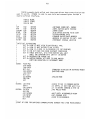
1
FTL REPORT R82-4
MTL COPY, DON'T REMOVE
33.412, MIT .... 02139
A PROGRAMMABLE PILOT ORIENTED
DISPLAY SYSTEM FOR GA AIRCRAFT
James A. Littlefield
May 1982
FTL REPORT R82-4
A PROGRAMMABLE PILOT ORIENTED
DISPLAY SYSTEM FOR GA AIRCRAFT
James A. Littlefield
May 1982
FTL REPORT R82-4
A PROGRAMMABLE PILOT ORIENTED
DISPLAY SYSTEM FOR GA AIRCRAFT
Abstract
This 1ape' presents a complete description of a digital flight
data processing platform designed to support a range of airborne or
flight simulator based experiments requiring the acquisition, processing,
and display of information. The Programmable Pilot Oriented Display
(PPOD) is based on IEEE S-100 bus standard equipment and readily available
software utilities. The design philosophy and techniques used to achieve
project objectives with a minimum of hardware/software customization
are discussed. System resources include three Z80 processors,
intelligent 10, complete interprocessor communications firmware, and
RS-170 composite video output. Discussion of both PPOD capabilities
and the steps required to employ PPOD in future experimental setups are
presented in the context of a mobile test run.
Aknowl edgements
The results presented in this paper could not have been achieved
without the individuals and organizations named below.
My advisors, Profs. A. Elias and W. Hollister, have provided technical advise, software expertise, and valuable suggestions throughout the
PPOD development effort.
Their digital data processing and flight
experience are partially responsible for the flexibility of the PPOD architecture. Prof. R. Simpson, Flight Transportation Laboratory director, has
supplied both a congenial working environment and many profitable insights
from his experience with pilot workload research.
Carter Pfaelzer, Al
Shaw, Don Weiner, Sue French, and Paul Wetzel have all contributed much in
the way of technical support and encouragement.
The research for this project was performed at the MIT Flight
FTL facilities and staff were important
Transportation Laboratory.
throughout the project.
Digital Marine Electronics Inc. provided one of
their Northstar 6000 Loran-C receivers for mobile testing.
The
Transportation Systems Center/DOT and especially Mr. William Wade are to be
thanked for providing a microprocessor development system during the early
stages of the PPOD project.
Funding for the development effort was provided by NASA Langley Research Center through the Joint University Program
for Air Transportation Research. (NGR-36-'109-017)
Table of Contents
Chapter
IV
II
III
IV
V
Page
Background and Introduction
System Hardware
The Interprocessor Communications Package
Software Development Utilities and Examples
Conclusions and Recommendations for Continued Research
References
Bibliography
Appendix AAppendix BAppendix CAppendix DAppendix E-
Software Listings
Hardware Modification Schematics
Jumper Setting and Customization Procedures
Processor Memory Allocation
Hardware/Software Vendors
86
87
91
116
123
127
131
5
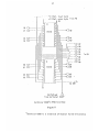
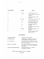
List of Figures
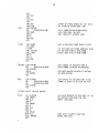
1.
PPOD Level I Objectives
13
2.
PPOD Level II Objectives
14
3.
PPOD Level III Objectives
16
4.
PPOD/Pilot/Aircraft Data Flow
18
5.
Task/Subtask Breakdown
20
6.
Simplified Mode 2 Interrupt Cycle
27
7.
145 Byte Data Transfers
31
8.
P1/P2 Communication Data Flow
32
9.
Interrupt Jammer r.2
33
10.
Data Port F2 Addition
11.
Loran Data Buffer Circuit
37
12.
Northstar 6000 Data Word Format
39
13.
GPIA Data Frame Format
40
14.
EPSCO Data Frame Format
43
15.
IUSER3. Variables and Flags
44
16.
IUSER3 Flowchart
46
17.
P1/P2 Communication Data Flow
53
18.
FUSER6 Variables and Flags
54
19.
FUSER6 Flowchart
55
20.
MACOD3 Variables and Flags
65
21.
MACOD3 Flowchart
66
22.
Mobile Test Run Data Plot
76
23.
RNAV User Command Set
77
24.
Navigation Equations for RNAV Program
79
25.
RNAV CRT Display
80
PPOD:
Programmable Pilot Oriented Display
A Digital Platform for Airborne Experimentation
Chapter I
Introduction and Background
The innovative application of advanced electronics to the needs of
the general aviation conmunity has been a slow process.
Economics, govern-
ment certification requirements, reliability considerations, and pilot
resistance are some of the factors which have caused this lag.
These
reservations have been aggravated by a scarcity of reliable experimental
information concerning control systems involving human decision making in a
hybrid man/machine environment.
Qualitative models of isolated sensory/
motor subsystem-s under rigidly controlled test conditions are available;
however, the performance of the human operator under any realistic task
constraint requiring the interaction of many sensory/control subsystems has
only been characterized in task specific terms.
This type of task specific
characterization does not lend insight into the internal functioning of the
human operator as a control loop element and thus is of limited usefulness
in anticipating human performance in an environnent only slightly altered
from that of the original test conditions.
Many instruments in use today,
especially in general aviation, trace their ancestry back to the early days
of aircraft development when the skies were not crowded and night or bad
weather operations were rare.
Before new display and other man-machine
interface technoloqies can, with confidence, be integrated into the cockpit
further quantitative and qualitative experiments oriented toward iathematical characterization of the pilot as a control element wil
be required.
Today, researchers in a variety of disciplines are actively pursuinq the answers to questions which have a bearing on instrument design.
This type of inquiry has taken on a particular urgency as the capabilities
of both airframe/power plant and electronics have continued to expand in
concert with a rapid increase in the demands placed on the pilot.
Of late,
particular attention has been focused on the transmission of data to the
pilot and the reverse process, means whereby the pilot can communicate his
The tradenames listed below are used throughout this paper and
belong to the indicated organizations.
MicroAngelo, Screenware PakI, Screenware PakII are
tradenames of the Scion Corp.
FCD-1,
1^2 are tradenames of Teletek Inc.
CP/M, PL/I-80, LINK-80 are tradenames of Digital Research Inc.
DM6400 is a tradename of Measurement Systems and Controls Inc.
Vedit is a tradename of CompuView Products, Inc.
Northstar 6000 is a tradename of Digital Marine Electronics Inc.
Z-80 is a tradename of Zilog Inc.
8080 is a tradename of Intel.
control outputs to the aircraft.
The pilot/instrument interface seems to
be one of the major bottlenecks in the aircraft control loop.
The limited
nature of the present day data paths between airplane and pilot first
became evident in military applications.
task such as
target acquisition,
Faced with a rapidly evolving
performance
of evasive maneuvers,
or
aircraft carrier landings the combat flyer must monitor a large number of
critical
parameters while simultaneously providing control outputs.
The
advent of STOL/VSTOL and ducted fan types of craft has also compounded the
difficulty of the control task in both the input and output areas.
In the civilian sector, pilots are increasingly required to adsorb
large amounts of data.
Crowded skies, a proliferation of navigation data
sources, and increased night/marginal weather operations have demonstrated
the inadequacy of many of the common techniques for presenting flight data.
As the necessity for increasing the capacity of the aircraft-pilot data
channel has been more clearly demonstrated,
more basic research has been
focused on the human operator and his input/output channels.
Results from
modern control theory have been combined with conclusions based on data
gathered from rigidly controlled experiments with human subjects to yield
mathematical models describing the internal functioning of the human operator.
In addition, information transmission theory and statistics have been
used to construct measures of channel capacity which can be applied to both
machine-machine and man-machine data links. The Shannon-Weiner information
measure provides a useful measure of data channel performance.
According
to this result information is quantized in units of bits with the information provided by an event 'x'
concerning event 'y'
given as I(x,y)=Log2
P( y)/P(x) [Ref. 1].
The utility of this measure has been deimonstrated in
a variety of experiments involving humans in control and pattern recognition tasks [Ref.
Although nost
1-6].
of the tasks described in the
experiments referenced are simple, they highlight many of the individual
characteristics which
are combined
in a complex task such as
vehicle
control.
Large budgets and more acute needs have placed the military and
commercial
manufacturers in the forefront of workload/human factors eng-
ineering research.
To date the techniques of this type of research have not
been extensively applied to the general aviation area.
Special
con-
sideration has only of late been given to the needs of the general aviation
In the past,
pilot flying in the single pilot IFR regime.
providing
general aviation with means of travelling with increased ease and safety
has been a subject of ongoing research by the participants of the NASA
Tri-University Program for research in Air Transportation.
the applicability
of
Loran-C
source holds
that this data
demonstrated
experience with Omega,
to general
Loran-C,
aviation
great
area
Recent work on
navigation has
promise.
Flight test
and preliminary work on Global Positioning
System Navstar combined with the previously mentioned needs for increased
channel capacity for pilot-craft links has provided the motivation for the
work reported in this paper.
matting, and processing
In the past much difficulty recording, for-
the output data from onboard experimental equip-
ment has been encountered.
Frequently pilots found extremely accurate
position information difficult to interpret because the display format wa's
unfamiliar
or
ambiguous.
These observations
demonstrated
that it is
possible to degrade overall
information if
pilot performance despite better situation
Ideally it
this data is presented in a confusing format.
should be possible to alter the presentation of flight information independent of the source of the raw data.
This
paper contains documentation
on
a flight data
processing
platform which provides a means of addressing all of the questions detailed
above.
The Programmable Pilot Oriented Display (PPOD)
project has as its
objectives, the creation of a digital flight data processing and display
system which supports the testing of both new navigation and new display
concepts.
An additional objective was to determine the extent to which
standard microprocessor technology could be conveniently adapted to the
airborne environment.
These goals have resulted in a development program
which differs considerably from market prototype production.
factors while still a consideration have been relaxed.
Size, weight,
Room for future
expansion and easy access for hardware maintenance/modification have taken
precedence over visual appeal.
Every attempt has been made to allow for
system upgrade and to support the greatest possible range of experiments.
Such a development philosophy can result in a device which presents the
potential user with such a bewildering set of features, options, and reconfiguration choices that overall device utility is minimal.
A major motiva-
tion for the use of standard hardware and proven software was the desire to
avoid complexity.
PPOD
and the documentation contained in this paper
constitute a compromise between ultimate flexibility and basic simplicity.
PPOD hardware, software, and the Interprocessor Communications Package provide a coherent operating environment in which it
is possible to design
This paper also provides a description of the boundaries to
experiments.
the
operating
environment
and
various
techniques
for
exploiting
the
available system capabilities to their greatest extent.
One
in
flight
function
of
PPOD
is workload
experimentation.
Especially critical for the evaluation of new display technologies is the
question of how the new medium affects the intelligability of the data
represented.
When a programmable link connects the data source with a CRT
the type of data presented to the pilot and the way in which this data is
shown can be altered in flight.
In addition PPOD is able to generate
secondary tasks or to contaminate valid flight data with extranneous visual
information
while
simultaneously monitoring
pilot's performance.
and recording the subject
Essentially PPOD functions as one of the primary data
paths between the pilot and his flight environment.
Since PPOD is program-
mable this data link can be artificially loaded until it
saturates or dif-
ferent display formats can be subjectively evaluated in a similar flight
regime.
In addition the information processed by PPOD can be recorded for
post flight analysis.
about the maximum
Similar techniques have yielded important insights
channel
capacity of the human
sensory system under
various conditions.
Initially PPOD will be used primarily for researching workload conditions in the single pilot IFR regime.
The experimental program has been
designed to progress through three levels of complexity.
These levels are
distinguished primarily
between
by the
type of communication
equipment and the digital processors residing in PPOD.
aircraft
Since each test
level contains a very large range of possible experiments, the test program
was not outlined as a schedule but rather as a conceptual breakdown enumerating three general classes of experiments which will be of interest in
the immediate future.
The first level involves no physical connections to
the aircraft except for power cables.
PPOD will function primarily as an
Through a series of ground simulations
electronic copilot at this level.
and flight tests, the extent to which an electronic scratchpad can aid a
pilot will be determined.
pilots
and
Especially in the GA single pilot IFR situation
are required to utilize information from charts, approach plates,
instruments,
controller.
as
as
well
heeding
the
instructions
of
a ground
A small computer with easy data/command entry and CRT display
tower frequen-
could provide a convenient method of organizing headings,
cies, takeoff or approach checklists, airport elevations.
Projected appli-
cations include fuel consumption and weight and balance calculations for
optimizing range.
An onboard real time clock will be used to schedule the
presentation of critical flight information.
PPOD can be instructed to
measure time intervals and remind the operator to check flight status when
a certain time has elapsed.
Storage of takeoff, landing, and emergency
procedure checklists is also anticipated.
The
second
instrumentation
to
level
involves one-way data channels from aircraft
PPOD's digital
10 ports.
This
level
from several
will
include
avilable data
automatic
selection of position information
sources.
Engine status although a desirable feature may not be tested
except in ground simulations.
available, it
Because a dedicated test aircraft is not
is not possible to conduct tests requiring modifications to
PPOD Lavel I Objectives
1.
Teal TLrwe Clock/Pacar Functions
a)
2.
Takeoff/Landing, Emergency checklists
a)
3.
4.
Deliver pilot promts on a preset schedule
during critical flight phases.
Autoatic checklist display/verify.
Storage of inforration pertaining to flight conditions
or destination
a)
Information available at operator request.
b)
Information displayed at a scheduled time.
Flight Computer Functions
a)
Cruise perfornance tables, takeoff distance, etc.
b)
Flight planning computations- fuel consumption,
wind corrections, weight and balance conputations
PPOD Level I Objectives
Figure 1
PPOD Level II Objectives
1.
Navigation
VOR, Loran-C, and other interface capability
a)
PPOD auto-selects from several data sources.
1)
Coordinate transfori-tion and display format.
2)
Multiple waypoint storage-- automatic switchover
b)
when way-point is reached.
Variable display forirat
c)
1)
2)
3)
2.
Flight Status Warnings
Engine/ Electronics
a)
Aircraft Configuration
b)
c)
d)
e)
3.
Mbving Map Display
-North Up Fbrrrat
Expanded Scale Fonrat
Airspeed, Stall warnings
Altitude Advisory
PPOD system fault detection/ self test
Other Functions
Kalrran filtering of navication data
a)
Enhanod IIS display rodes
b)
DABS message display, weather data
c)
PPOD Level II Objectives
Ficure 2
the instrument panel or the mounting of remote sensors in the enqine compartment.
To date most of the development work has been directed to this
second level.
Presently a Northstar 6000 Loran-C receiver is being used in
a test level
two mode.
PPOD has been programmed to monitor two data
channels which the receiver multiplexes onto a single data bus.
Based on
signal to noise thresholds PPOD automatically selects the channel which
provides the best position information.
The raw data in the two channels
provides enough information to compute position, estimated time of arrival,
and ground speed.
variables.
An enroute navigation display is generated from these
Eventually this data will be applied to final approach and
enhanced ILS displays as well.
The third level
interactions
of test complexity is characterized by two way
between PPOD and
the on board
equipment.
Although
PPOD
already contains the processing power necessary to handle rudimentary automatic control functions, a great deal of work remains before any significant experiments at the third test level can be conducted.
Instrumenting
an aircraft with sensors which would allow PPOD to monitor all aspects of
the flight will be a time consuming task.
If a digitized measure of fuel
flow were available the data could be combined with navigation data to compute projected range.
will
As modern autopilots are providing digital ports, .it
be possible to connect PPOD
course following ability.
to these devices providing automatic
Digital tuning of nav/com receivers is another
application to which PPOD is well suited.
are very expensive, costs are dropping.
Although scanning DME receivers
Coupled with the processor speed
and 10 flexibility of PPOD one of the scanning DME receivers would provide
a wide coverage RNAV dependent only on an existing network of transmitters.
PPOD Level III Objectives
PPOD/Autopilot Link for automatic course following
Message Downlink capability
Avionics frequency/rrode control
a)
Automatic selection of Loran chain and stations
based on SNR and grid orthogonality considerations.
b)
Digital tuning of conventional Nav/Com receivers.
PPOD Level III Cbjectives
Figure 3
Although lack of a dedicated test aircraft has limited the type of
experiments done to date,
PPOD has been designed to support a long range
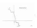
flight test program encompassing all of the levels mentioned above.
simulation work
is not correspondingly
limited.
Extracting
Ground
flight and
engine status information from a simulator is electrically simpler and does
not compromise flight crew safety.
Some work has been done with simulated
landings using a prototype ILS display generated by PPOD and driven by
digitized
position signals from
within the analog simulator
(Ref.
7).
These experimehts have demonstrated that the combination of analog flight
simulator,
PDP-11/10 computer,
satile simulation setup.
and PPOD represent an expensive yet ver-
The PDP-11 can be used to simulate the digital
outputs from navigation devices ranging from VOR to Loran-C to scaning DME.
In addition the PDP-11 could be used to generate digitized engine status
data.
Digitized information whether artificially generated or based on
flight simulator outputs can then be fed to PPOD for processing and display
generation.
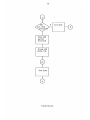
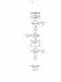
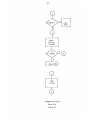
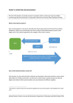
A human subject completes the test control loop as shown in
figure 4.
The level I,
in determining
the
II,
III test plan organization has served as a guide
required capabilities of the hardware and software
included in the PPOD system.
different performance it
Since the experiments at each level demand
was necessary to select several component sub-
systems able to support the experimental objectives and to operate in a
conceptually
straight
forward
fashion.
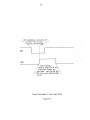
The PPOD system architecture
reflects the underlying structure of the objectives mentioned above.
underlying task structure
This
dictated a modular approach at the hardware/
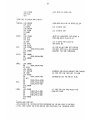
00,
Loran
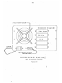
CRT
PPOD
PPOD/Pilot/Aircraft Data Flow
Figure 4
VR/DME
GPS
firmware level of system integration.
Following the outline of the test
program the choice of hardware and software utilities was reduced to selection of conponents able to perform
10 formatting and data acquisition,
coordinate conversion and arithmetic processing, and finally generation of
video output.
The rich array of experiments,
jected, is dependent on this modularity.
both in progress and pro-
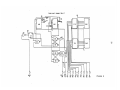
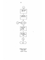
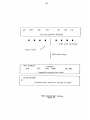
PPOD actually consists of three
Z-80A CPU chips and support circuitry hereafter designated PO,P1,P2.
In
any of the operational modes PPOD's task can be divided into three distinct
subtasks; 1)-data 10,
2)-
control-coordinate conversion-number crunching,
and 3)-video display generation.
PO,P1,P2 are assigned to each of these
three subtasks as illustrated in figure 5.
PO handles storage, formatting,
and control functions related to the two 8 bit bidirectional data ports, 16
latched control output lines,
handle reformatting
passed to P1.
PO may also
and transmission error checking before the data is
All code dependent on the 10 format of the device being
tested in allocated to PO.
units.
and 12 status input lines.
P1 has the most general task of the three
Pl's duties include coordinate conversion, generation of commands
to PO and P2, user data entry processing, and synchronization of the operation of all three CPUs.
P1.
Hardware failure detection is also allocated to
P2, the video processor, accepts commands mainly from P1 although it
can also handle light pen inputs.
P2 generates a bit map containing the
picture information based on these graphic command inputs.
Division of a task among three CPU's
increase in system throughput.
has as its main advantage an
This throughput improvement,
however,
is
highly dependent on task organization and interprocessor resource sharing.
PPOD PROJECT-- INTERPROCESSCR COMMUNICATrIONS
Task/Subtask Breakdown
NAVAID------->
I
IO
formatting
TASK
.
-
>
PILOT
-
I
MMPE and
coordinate conversion
Processor 0
Processor
IA2*
FDC-I*
Figure 5
I
iVideo displayl
generation
Processor
MicroAngelo*
Care must be taken in the design of any multiprocessor algorithm to ensure
that two processors do not attempt to access the same portion of memory at
the same time.
It is desirable to exploit the maximum concurrency in any
given task; however, this objective must be balanced against the possibility of resource conflicts.
systems
Modern nultiprocessor
employ
spe-
cialized software to maximize system throughput without incurring resource
The control task is generally divided between two specialized
conflicts.
A control portion of the code adapted to synchroniza-
pieces of software.
tion of the processors functions in an executive capacity allocating memory
space and peripheral access time.
an execution lattice.
The executive is in turn controlled by
Each task given to a multiprocessor is divided into
A subtask is allocated to each processor.
subtasks.
The execution lattice
contains all information relating to the order in which the subtasks can be
Following the structure of the execution lattice, the executive
performed.
enforces the
currency
sequencing of subtask execution so that the maximum con-
of the job
is
exploited
without
causing resource conflicts.
Extremely careful analysis of the job is required to produce an efficient
execution lattice without creating these conflicts.
Considerable skill is
required to divide a job into a series of efficiently executing subtasks
and create the proper execution lattice and executive.
The expertise and
effort required for truly flexible multiprocessing have led to the adoption
of a simpler approach in PPOD architecture.
commodities
in any multiprocessor network are memory and communications
channel capacity.
each CPU,
Generally two of the scarcest
Since PPOD's processors have memory areas reserved for
the communications resource is a more critical constraint.
Interprocessor Commmunications Package (IPCP)
An
has been implemented to ease
this constraint.
This body of firmware is written in assembly language but
can
from high
be accessed
level
languages.
Thus
the multiprocessor
hierarchy is largely transparent to the experimenter despite the potential
for vastly increased throughput which results.
The preceding pages have desribed some of the experiments which
PPOD makes possible.
Considerable effort has been put into creating a
basic structure of compatable hardware and software forming a skeleton upon
which high level expe'riments can be based.
Because the capabilities and
limitations of PPOD are to a large extent defined by the interaction of the
submodules outlined above the remainder of this paper is devoted primarily
to their documentation.
Subsequent chapters will detail the hardware and
software associated with each submodule or task element.
Chapter II
System Hardware
PPOD hardware consists of a variety of S-100 bus compatable cards,
an S-100 mainframe, keyboard entry device, and CRT.
inch floppy disk drive, video terminal,
software development.
Hardware
In addition" a dual 8
and line printer are used during
selection was based on the following
criteria: versatility, low cost, ease in system- upgrade, reliability, low
power consumption.
A secondary consideration affecting choice of com-
ponents was size.
The GA aircraft places severe space restrictions on
avionics.
While these space considerations are less important
research application,
in a
every attempt has been made to integrate several
functions into a single board thus reducing power use and keeping motherboard slots open for future experimental projects.
PPOD hardware resides in a metal case containing a 12 slot motherboard, AC power supply, and cooling fan.
Forced air cooling is required
for several of the logic cards because of the high component density.
circuit breaker is included in the power-on switch.
A
No front panel
controls are available to the user except for a system reset button.
Connectors
for two RS-232-C
serial ports with handshaking lines, disk
drive, composite video, and parallel port are provided at the back of the
cabinet.
Cabinet dimensions are approximately 12X8X18 inches.
The AC input power supply is sufficient for all laboratoy simulation and software development work.
For flight tests a 300 watt DC/AC
power inverter is used.
The inverter unit takes as input 10-18 volts DC
and supplies 120 volts 60Hz output.
Some undesirable characteristics of
the power inverter are its square wave output and the inefficiency inherent
in two levels of voltage conversion.
The harmonics in the square wave
power output do not effect the digital logic but increased jitter in CRT
images has been observed.
reception if
This noise source does not affect the Loran-C
care is taken to ground the receiver.
Both electrical waste
and the added weight of a combined DC/AC power inverter and AC/DC power
supply could be saved if
volts and +/-
an airborne power supply capable of supplying +8
16 volts DC was available.
At present attempts are being
made to locate a manufacturer who will supply a switching power supply of
sufficient wattage.
Switching supplies achieve efficiencies in excess of
90% and are capable of both step-up and step-down operation.
Because of
the low dissipation in a switching supply and the absence of a large trans-former,
switching supplies are generally smaller and lighter then conven-
tional power sources of the same wattage.
These properties recommend the
switching unit for airborne applications where excess weight
is to be
avoided and electrical power is not abundant.
Resources of the system are divided among the three processors.
Each processor and support circuitry resides on a standard bus card.
addition two memory cards,
attached to the bus.
In
a 64k dynamic RAM and a 32k EPROM card, are
There are several different standards for arranging
the power and communication connections in digital systems consisting of
several physically separate units.
for several
reasons.
The S-100 bus standard was preferred
Of primary importance was the popularity of this
particular bus with the manufacturers of the subsystems required for a
complete
microcomputer system.
communications
lines
The S-100 bus supplies a greater number of
between
the
devices
attached
to
the
bus.
Compatability with newer 16 bit microprocessor chips was also an important
consideration.
PO,
the 10 processor, has 2k dynamic RAM and 2k EPROM which con-
tains a control
access (DMA).
program.
Data transfers to P1 are via direct memory
PO is capable of transferring up to 1k bytes and can access
or store data anywhere in the P1 memory map.
PO directly controls two 8
bit bidirectional data ports, two 6 bit status input ports, and two 8 bit
latched control output ports.
In addition status and control/command bytes
can be passed between P1 and PO through data port 04FH.
PO can communicate
with peripheral devices either through the terminated status input lines or
by Z-80 mode 1 interrupt.
The factory supplied 10 routines have been
patched at location 068H and a jump to scratch pad RAM placed at this
address.
Any interrupt to PO will vector directly to the jump instruction
at 068H.
The user is expected to insert the appropriate device handler at
the target address of the jump instruction.
P1,
the main processor responsible for numerical work,
coordinate
conversions, and subtask synchronization utilizes a full 64k address space.
A Measurement Systems and Controls 64k dynamic RAM board and a 32k EPROM
card
fill
the
P1
address
space.
The
RAM board
supplies
on
board
transparent refresh eliminating the need for external refresh generation
circuitry.
RAM and EPROM can be overlayed in blocks as small as 4k; RAM
can be deselected in blocks ranging from 4k to 32k; EPROMs can be individually enabled or deselected.
directly on the P1
board.
An
additional
4k
of memory
is located
This memory block extending from FOOO-FFFF con-
sists of two 2716 EPROM sockets.
Memory address conflicts between P1
onboard memory and off board RAM or EPROM are automatically resolved by P1
unnecessary to deselect off board memory from
address decoders making it
A block of 4k RAM (FOO-FFFF)
FOOO-FFFF.
by P1.
exists which cannot be accessed
Essentially there is an additional 4k RAM available to any pro-
cessor capable of sharing P1 memory.
One of the two EPROM sockets on board
P1 is occupied by a 2k monitor supplied by the manufacturer.
provides
assembly
language
subroutines
for
basic
This monitor
communication
with
P1 has access to two serial ports, one and a half parallel
peripherals.
ports, and up to eight floppy disk drives or an intelligent hard disk.
real
time
clock is
also
implemented.
Standard
Zilog interrupt
chaining is employed for all interrupt sources on board P1.
permits
nested
interrupt execution.
interrupt enable out (IEO)
The
daisy chain
and interrupt enable in (IEI)
A
daisy
This scheme
control
signals
are available at
the parallel port B connector for adding other boards or external devices
to the low priority end of the daisy chain.
Interrupt daisy chaining is
fully documented in the Zilog product descriptions and applications notes
for the
interrupt
Z-80
SIO,
PIO,
and
CTC chips.
P1 utilizes the Z-80 node 2
protocol.
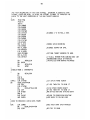
A time history of a mode 2 interrupt sequence is
shown in figure 6.
A low level on the processor INT line indicates an
external device is requesting attention.
the
position
of the
requesting
Device priority is determined by
device in the daisy chain.
The CPU
acknowledges the interrrupt request by raising the INTA, bus pin number 96,
CPU completes execution of
'.
current instruction
before a'cknowledge,'
INT
INTA.
Interrupting
device puts its 8 bit',
,' interrupt vector on
,'
the data
bus during the
\
CPU interrupt acknowledge
cycle.
Simplified Mode 2 Interrupt Cycle
Fi gure 6
to a high level.
Upon receipt of the INTA high level,
device places an 8 bit interrupt vector on the data bus.
the interrupting
This interrupt
vector is combined with an interrupt table base address to yield a 16 bit
absolute memory address.
tial
location contain
interrupting device.
The contents of this address and the next sequenthe 16 bit address of the code to service the
Although the mode 2 interrupt level requires more
hardware and involves more critical timing than the mode 1 interrupt level
employed by PO,
the mode 2 level supports a greater number of interrupt
sources and the location of the individual service routines can easily be
altered since the table of service routine addresses resides in RAM.
P1 runs at 4 MHz clock speed.
board
Jumper options on the processor
program the unit to automatically insert 1 wait state for all on
board memory access.
Any reference to locations in the range FOOO-FFFF
automatically generates a wait state.
The 32k EPROM card generates 1 wait
state independent of processor wait state mode.
P1 and support circuitry consists of a Teletek FDC-1 r.2.
In addi-
tion to the jumper settings which are fully documented in appendix C,
several slight modifications have been made to the P1 card.
require that the S-100 address,
data,
status,
DMA operations
and control lines be tri-
stated according to rigidly specified bus timing instructions as part of
the transfer of control to a temporary bus master.
The stock FDC-1 r.2
unit does not handle the transfer of bus control properly.
Two minor manu-
facturer suggested modifications were performed to correct this problem.
The changes are fully described in appendix C.
Future revisions of the
FDC-1 processor card should not require this alteration.
P2, the video processor, is a Scion Corp.
graphics board.
MicroAngelo monochrome
This unit accepts command bytes at port OFOH and provides
status information at OF1H.
In addition, provision is made for a light pen
graphic input however this feature is not utilized at present.
Outputs
from the MicroAngelo board are both direct drive and composite video.
graphics package is supplied by the manufacturer.
The graphics routines
are contained in two 2k EPROMs and are described in chapter III.
are provided for two additional EPROMs.
A
Sockets
This extra space is reserved for
the addition of extensions to the originally
supplied graphics primitives.
Scion Corp. is marketing a 4k extension, PAKII, which includes a variety of
curved primitives.
The suggested method of communication between a host system, in
this case P1, and the MicroAngelo board,
P2,
is a polled method in which
the host reads the status port, OF1H, and passes a command byt'e to the data
port, OFOH, when a ready condition is detected.
The objective of this com-
munication method is to prevent host command bytes from being written over
each other in the MicroAngelo communication buffers.
In an application
where large amounts of data are to be transmitted from host to video unit a
great deal of time can be lost in polling the P2 status port.
This wasted
time translates into decreased system throughput since the host processor
and the video processor are both tied to the communications task.
Another
negative feature of the polled interface is that the waiting time between
commands
is a function
of the execution speed of previous commands.
During execution of code with timing constraints entry into an idling loop
could adversely affect performance.
For these reasons a buffered interrupt
driven Interprocessor Connunications Package (IPCP)
has been written.
The
two communication protocols are diagrammed and compared in figures 7 and
8. The firmware aspects of the IPCP will
be explained in a subsequent
chapter.
MicroAngelo only supplies status information at port OF1H. Jumpers
are provided to patch the status signals to the vectored interrupt lines
of the S-100 bus however P1 expects all interrupts to conform to Z-80 mode
2 specifications.
To remedy this inconpatability the interrupt jammer
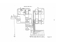
diagrammed in figure 9 was created.
Jammer circuitry monitors the S-100
INT, INTA lines, the P2 status lines, and the P2 status port.
Whenever P2
status port bit 0 falls to a low level indicating a ready condition, the
jammer latchs an interrupt request pending signal.
The D FF and nand gate
save this pending interrupt until all prior interrupts are no longer being
serviced.
P2 interrupt request is then latched by the upper S-R flip-flop
which passes the request to the S-100
bus interrupt line.
S-100 INT is
held at a low level until an INTA signal from P1 indicates that the request
has been aknowledged.
The rising edge of INTA clears the interrupt request
and enables the outputs of two 74LS173s which are connected directly to the
S-100 bus.
bus.
An interrupt vector unique to P2 is thus placed on the data
INTA falling edge disables the 173s freeing the data bus for other
operations.
74LS221 dual monostables have been used for edge/level and
level/pulse conversions.
An S-100 compatable prototyping card carries all
of the jammer hardware.
Communication between P2 and the jammer card is
via vectored interrupt line 0, S-100 pin 4.
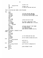
PPOD PROJECT------INTERPROCESSOR
Ft
COMMUNICATIONS
Status
FDC- i*
Microangial1*
M
F0
Data
Single byte data transfer
145 bytQ data transfers
Figure 7
Main processor (Pl)
Graphics
Firmware
115 byte command buffer
Port 04FH
Read Strobe
Inbound
(HCBF)
data latch
-7
Interrupt Janner
Interrupt
Vector
L-------
Pl/P2 Communication Data Flow
Figure 8
Interrupt Jamer Rev.2
00
-
HCBF
4
+5
INTA INT 07
96 73 43
9605 D4'03
93 92 91 42
02
41
Dl
94
950
449
Figure
Fgr
Addition of the jamming circuit to the graphics board as purchased
from the manufacturer provides system users with a second high speed method
of passing data from P1 to P2.
In depth analysis of optimun use conditions
for the two protocols is postponed until chapter III.
A second hardware
addition to the P2 processor communications circuitry allows the video
board to receive data/command information via data port OF2H in addition to
port OFOH.
Addition of the circuit shown in figure 10 was motivated by a
need to support a high level graphics command set capable of suspending any
lower level command execution.
Use of the added data port will be detailed
in a later section.
Remaining
hardware
graphic output screen,
items
are
the
inflight
and development console.
data
entry device,
Any video terminal uti-
lizing RS-232-C standard data transmission can be used in the laboratory.
Graphic and alphanumeric output from P2 is displayed on a 9 inch diagonal
The display phosphor is P31,
Motorola monitor.
sistance green
phosphor.
for the video monitor.
12 volt DC as well.
a relatively long per-
Both 120/220 volt AC power settings are standard
The unit used with PPOD has been modified to accept
In flight data entry is through a full size alpha-
numeric keyboard. Such a unit is not practical for pilot data entry on production equipment where an 8, 12
number of inputs.
, 16 key unit provides the necessary
PPOD's research orientation demands a full size keyboard
capable of modest inflight system reconfiguration.
the P1 card is used for keyboard input.
directly from the P2 processor card.
The 8 bit PIO port on
Power for the keyboard is taken
P2 Hardware Modification
U44 Pin 1
U45 Pin 11
-
'LS367
P2 Data Bus
Bit 4
U29 Pin 1
B
-
U9 Pin 9
U29 Pin 11
U53 Pin 11
Modification Procedure
Cut trace from U45 Pin 9 to U29 Pin 11
Cut trace from U45 Pin 9 to U53 Pin 11
Connect remaining jumpers as indicated above
NOTE:
All IC designations for this figure correspond
with those of the P2 (Scion Corp. MicroAngelo)
user's manual.
Data Port F2 Addition
Figure 10
Chapter III
The Interprocessor Communications Package
Complete subroutines for data transmission between the processors
are provided by the Interprocessor Communications Package (IPCP)
firmware.
IPCP routines are divided into task dependent routines and those which may
be used in any experimental setup.
The PO control program represents the majority of the task dependent code.
Specific input device formats,
rudimentary calculations, and
data stream filtering are tasks which vary from device to device. A specific control program example is given below to illustrate the utility of the
parallel processor hierarchy and the method of communication between P1 and
P0.
Digital data from a Northstar 6000 Loran-C receiver has been used
in a series of experiments.
The Northstar supplies a serial output data
stream at a rate of approximately 75,000 bits per second.
By taking data
out of the receiver at the input to a parallel to serial converter, a
series of 15 bit words at a lower data rate of 5000 words/sec.. can also be
taken from the receiver.
The format of these words and a sample digital
recording of position are given below.
Fifteen bit words are multiplexed
into one of the PO 8 bit input ports by two of the PO control output lines.
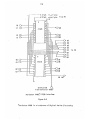
Figure 11 shows the hardware used to buffer the receiver data bus and perform the multiplexing.
lower byte
upper byte
]-<Sel.
] Sel.
f-oin PO
9 +5
D1 L -
10
12
13
] A2
74374
- -
]AAI
3>~~~
~A0
-
1
HH
----- {i~07
>
06
-- T
05
04
fL
I h>
>
D2 E>----D
C>---
D3
~-~
~
-
C
-- -4
--
74374
_PO
01
00
D6
5
.~~~cJC
-
To PO
02
T
e
DO
03
D4*
.
INT
Shift/Load-
from Northstar 6000*
Northstar 6000*/ PPOD interface
figure 11
*
Northstar 6000 is a tradenamae of Digital Marine Electronics
Each 15 bit word is composed of 8 bits of data, 3 bits of address
(which device the data is sent to),
figure 12.
and 4 identification bits as shown in
Four devices external to the Northstar 6000 can be addressed.
Each device is expected to observe the address bits of every data word and
latch those which are sent to it. For the purposes of mobile testing it
was desired to consider data from two of the four available devices.
required data streams are those for the GPIA (address 010)
EPSCO plotter (address 001).
The
and for the
A GPIA data frame consists of 27. bytes con-
taini'ng time differences, latitude and longitude, and auxilliary data for
one of the stations in the Loran-C chain being monitored.
provides signal to noise ratio,
mode number for each station.
slave (Sl)
Auxilliary data
envelope cycle discrepancy,and tracking
Latitude and longitude is based on the first
and the second slave (S2)
time differences (TDs).
TDs and
lat/long are available about once every 2.7 seconds with auxilliary data
stations in a given Loran chain available once every 16 seconds
for all
[see fig. 13].
EPSCO data frames consist of 12 bytes giving S1 and S2 TDs
in binary coded decimal [see fig. 14].
These data frames are available
about once every 2 seconds. A higher update rate is preferable so whenever
S1,
S2 TDs are reliable EPSCO data should be sent to P1 for further pro-
cessing.
Low SNRs as indicated by auxilliary data from the GPIA stream
require a reversion back to the longer although slower data stream.
All communication between PPOD and the Northstar 6000 is handled by
PO which is in turn directed by its control program.
IUSER3,
the
is flowcharted in figure 16.
sequence described below.
This control program,
Control program processing follows
Latching of a new
15 bit word at the
Northstar 6000 Data Word Format
Data representation inside the Northstar 6000 Loran receiver is as
shown below.
These data words are available in serial form at the
receiver digital output jack and can also be accessed in parallel directly
from the receiver's internal data bus.
<A2><A1><AO><I3><I2><I1><IO><D7><D6><D5><D4><D3><D2><D1><DO>
Where
A2-AO determine which of four possible output devices
is being addressed. .
13-10 identify which word in the device data frame
is being transmitted (see device data frame formats).
07-DO contain the data for the device and word specified by
the contents of the A and I fields.
Figure 12
Ref. Digital Marine Electronics Corp.
"Northstar 6000 Remote Serial Data Format"
Northstar 6000 GPIA Data Output Format
Word Nunb er
Identification Bits
Content
1.
F
GRI count (16 bit binary, MSB)
2.
0
GRI count (16 bit binary, LSB)
3.
0
TD1 (24 bit binary, MSB)
4.
0
TD1 (24 bit binary)
5.
0
TD1 (24 bit binary, LSB)
6.
0
TD2 (24 bit binary, MSB)
7.
0
TD2 (24 bit binary)
8.
0
TD2 (24 bit binary, LSB)
9.
0
TD3 (24 bit binary, MSB)
10.
0
TD3 (24 bit binary)
11.
0
TD3 (24 bit binary, LSB)
12.
0
TD4 (24 bit binary, MSB)
13.
0
TD4 (24 bit binary)
14.
0
TD4 (24 bit binary, LSB)
15.
0
Latitude (8 chars, Packed BCD)
16.
0
Latitude (8 chars, Packed BCD)
17.
0
Latitude (8 chars, Packed BCD)
18.
0
Latitude (8 chars, Packed BCD)
19.
0
Long. (8 chars, Packed BCD, MSB)
20.
0
Longitude (8 chars, Packed BCD)
21.
0
Longitude (8 chars, Packed BCD)
22.
0
Long. (8 chars, Packed BCD, LSB)
23.
(See Note)
Auxilliary data
Figure 13
Sheet 1/3
NOTE:
24.
Auxilliary data
25.
Auxilliary data
26.
Auxilliary data
27.
Auxilliary data
Identification bits for auxilliary data determine which of the
following formats applies.
Identification Bits
Content
1
Master auxilliary data
2
TD1 auxilliary data
3
TD2 auxilliary data
4
TD3 auxilliary data
5
TD4 auxilliary data
6
Common data
Master and TD auxilliary data is given in the following format.
Byte
Content
23
Cycle warning, mode (C---MMMM)
24
SNR, 2 words, 10 bit binary in form (OOOSSSSS)
25
SNR,
26
Blink SNR,
27
Blink SNR, 10 bit binary (SSSSSOOO)
(SSSSSOOO)
10 bit binary (OOOSSSSS)
Common auxilliary data is given in the following format.
Byte
23
Content
Manual cycle flag (0= manual cycle)
Figure 13
Sheet 2/3
24
GRI, 16 bit binary MSB
25
GRI,
26
Not used
27
Not used
16 bit binary LSB
GPIA Data Frame Format
Figure 13
Sheet 3/3
Ref.- Digital Marine Electronics corp.
"Northstar Remote Serial Data Format"
EPSCO Plotter Data Frame Format
Information is transmitted from the Northstar 6000 receiver to the
EPSCO plotter in a series of data frames.
Each data frame consists of the
following sequence of words
Word Number
Identification Bits
Contents
1.
000
RESET command
2.
001
Rightmost digit-1
3;
010
Digit 2
4.
011
Digit 3
5.
100
Digit 4
6.
101
Digit 5
7.
110
Leftmost digit-6
8.
111
LOAD command
13 is zero for the first slave TD and one for the second
slave TD.
Each TD is encoded in BCD with one digit per data word.
Figure 14
Ref.-Digital Marine Electronics Corp.
"Northstar 6000 Remote Serial Data Format"
IUSER3 Variables and Flags
The Northstar 6000 interface code can be configured in several different- ways. The various options can be selected by the user at source
code assembly time by programming the control/status variables listed
below.
STATWD(1293)--The STATWD provides bits for passing status information
between parts of the program.
Bit
Bit
Bit
Bit
0:
1:
2:
3:
Bit
Bit
Bit
Bit
4:
5:
6:
7:
H-->A GPIA frame is being accumulated.
Reserved for future use.
H-->A GPIA frame is ready for tranmission to host.
H-->SNR levels for first and second slaves
are above required thresholds.
H-->An EPSCO frame is being accumulated.
Reserved for future use.
H-->EPSCO frame is ready for transmission to host.
Reserved for future use.
SNRWD(1206)---The SNRWD indicates the history of the SNR levels for the
first and second slaves.
If both SNRs were above the
required minimum level then both bits 1,2 will be high.
If
either bit is low then one of the stations is not being
received well and the full GPIA data frame should be passed
to the host.
Bit 0: H-->Next
data
Bit 1: H-->Last
Bit 2: H-->Last
byte from receiver will contain SNR
for either S1 or S2.
SNR checked was above the required minimum.
SNR checked was above the required minimum.
CONWD(1205)---The CONWD location controls the type of data sent from
PO to P1.
The IUSER3 control program can decode either
EPSCO or GPIA data frames, decode both types of data,
or select the optimal data frame based on SNR criteria.
Figure 15
Sheet 1/2
Bit 0: H-->Decode GPIA data.
Bit 1: H-->Decode EPSCO data.
Bit 2: H-->Decode the best data based on SNR levels.
The remaining named locations in the source code listing pertain to
features of the PO hardware and are fully documented in the user's manual
for that processor.
Figure 15
Sheet 2/2
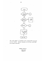
IUSER3 Flowchart
Figure 16
Figure 16 Cont.
Figure 16 cont.
Figure 16cont.
PO enables the outputs of the
receiver produces a mode 1 interrupt to PO.
high order latch, reads the contents of the latch, and examines the address
bits.
If
the device address is not EPSCO or GPIA then no further pro-
cessing occurs.
placed in a
If address bits are correct then the data is
is stored for subsequent processing.
a ring buffer where it
PO places the
high order latch outputs in the high impedence or disabled condition and
enables the low order output data which is also placed in the ring buffer
at the location immediately following the high order byte.
Enough space in
the ri'ng buffer is'allocated to contain two entire frames, one of EPSCO and
one of GPIA data. Thus,
the buffer will be filled once every 2.7 seconds
under normal operating conditions.
storage location
Use of the ring buffer as a temporary
for incoming data significantly relieves the software
timing requirements.
The double buffered scheme allows processing to con-
tinue during the gaps when no data is being transmitted from receiver to
PO.
Idle time is used to process any bytes in the ring buffer.
Once data has been placed in the PO ring buffer processing is
synchronous.
A read pointer (RP), a write pointer (WP), and a count of the
number of bytes waiting to be processed (BTG02) indicate the buffer status.
Sequential
processing continues until
no bytes are left in the buffer.
The synchronous portion of the control program reads each data word from
two successive locations in the ring buffer, determines the device address
and
enters
the
appropriate
processing
subroutine.
EPSCO
data
is
transmitted with plotter control commands preceding and following each TD.
The EPSCO data routine deletes these command
P1.
bytes from the data sent to
GPIA processing code assembles complete GPIA data frames.
Length
checking is done on each frame to make sure that noise has not introduced
extranneous bytes or caused a byte to be lost.
compared with the S1,S2
SNR limits are continuously
SNR values embedded in the auxilliary data portion
of GPIA frames.
When sent to P1,
both GPIA and EPSCO frames have as the first byte
a special tag indicating whether the contents of the frame are EPSCO or
GPIA.
All data transfers are by DMA operation.
The DMA target address in
the P1 memory space can either be set at assembly time or dynamically
changed by a sequence of command bytes sent to the PO command/status port,
04FH.
Before sending a fresh data frame to P1, PO checks to see if the DMA
target address location contains a non-zero value.
If the target address
contains zero then P1 is done with the last data frame and the DMA operation is completed.
If the target address location contains a non-zero
value then the previous frame is still being processed and PO begins accumulation of another data frame.
is provided by the CONWD.
GPIA devices.
Another degree of communications control
Various bits control the decoding of the EPSCO,
Bit 0 high enables GPIA device decoding, bit 1 high enables
EPSCO decoding, bit 2 high causes conditional decoding of either EPSCO or
GPIA device channels according to the SNR criteria mentioned previously.
Task independent code consists primarily of FUSER6.
code passes command bytes to P2 from P1.
This body of
P1/P2 communications occur either
according to the manufacturer suggested polled mode or by an interrupt driven mode.
Operation of the polled transmission link has been described.
To pass a command byte to MicroAngelo, P2, via the interrupt driven link,
all the user must do is place the byte to be transmitted in the A register
and call an FUSER6 subroutine named OUTBT.
OUTBT places the command byte
to be sent to P2 in a 115 byte first in first out (FIFO) buffer.
cess is illustrated schematically in figure 17.
This pro-
FIFO buffer addresses are
stored in the form, base address + offset, so the entire buffer is easily
relocated in memory simply by changing the buffer base address.
Buffer
organization is preserved by two pointers; the write pointer location indicates the offset from base address of the next empty location in the
buffer; the read pointer contains the offset from base address where the
next byte to be read and transmitted to P2 is located.
The difference mod
115 of the two pointer values is the number of bytes currently waiting to
be sent to P2.
Number of bytes left in buffer is stored in a separate
BTGO.
The FIFO is defined to be empty when BTGO=0, i.e. both
location,
read and write pointers are indicating the same location.
In addition to
the 115 byte FIFO created in P1 memory space an equivalent FIFO
P2 memory.
exists in
Thus a total buffer space of 230 bytes is reserved for command
storage.
Consider an example in which it
is desired to create a moving map
display or some other form of visual output which evolves in real time.
Assume that new data is available every 2 seconds as with the Northstar
6000 and that a new map indicating position.with respect to certain landmarks is to be generated with each position update.
In addition the entire
map requires 200 bytes to specify (200 bytes = 40 vectors).
Since vector
generation routines are among the slower elements in the manufacturer
supplied graphics
package,
P1 will
load up the 115 byte FIFO buffers.
Before placing a byte in the FIFO P1 checks to see if
BTGO is zero.
If
Main processor (Pl)
P2
Graphics
Firmware
115 byte command buffer
FUSE R6
8
Interface
routine
Port 04FH
8
Inbound
data latch
Read Strobe
(HCBF)
8 1
-&-8'---,-
Interrupt
Vector
Interrupt Janner
L--------------------------
Pl/P2 Communication Data Flow
Figure 17
Variables and Flags for FUSER6
TDF(EFC3)-
A non-zero value stored at this location enables software
performance monitoring code embedded in the P1 real time
clock interrupt service routine.
RPA(E7F1)-
This location serves as a read pointer and contains the
offset from buffer base address of the next command byte
to be read from the ring buffer and transmitted to P2.
ERRCNT(E6FF)- If enabled the software performance monitor code will
store the number of errors detected and corrected since
system start in this location.
BTGO(E7F2)-
BTGO contains the number of bytes in the ring buffer
waiting to be transmitted to P2.
BASE(E7F4)-
BASE is the base address of the ring buffer. All buffer
operations occur relative to memory locations which are
addressed as offsets of this base address.
START2(F852)- Location of the start of the routine to service the
interrupts generated when P2 requests another command
byte from the P1 ring buffer.
CNTST(E7F3)-
Flag/status variable. Bit functions are as follows..
Bit 0- H->Next attempt to put a byte in buffer will fail
L->Next attempt to put a byte in buffer will not fail
Bit 1- H->Ring buffer is full
L->Ring buffer is not full
Bit 2- H->Buffer is non-empty and transfer is in progress
L->Transfer is not in progress
Bit 3- H->Check bit used for error recovery processing
Bit 4- H->Use buffered transfer mode
L->Use polled transfer mode
Bit 5- H->Reserved for future use
L->Reserved for future use
Bit 6- H->Buffer control bit used to synchronize buffer
emptying operation when an overflow condition occurs
Figure 18
FUSER6 Flowchart
Sheet 1/4
Figure 19
56
FUSER6 Flowchart
Sheet 2/4
Figure 19 Cont.
FUSER6 Flowchart
Sheet 3/4
Figure 19 Cont.
FUSER6 Flowchart
Sheet 4/4
Figure 19 Cont.
BTGO is in fact zero then P1 will write the byte to P2 ccamand port OFOH.
Since P2 has a second 115 byte FIFO in addition to P1's command buffer,
FUSER6 will pass the first 115 bytes written into the P1 command buffer
directly to the P2 command buffer.
When P2's FIFO is full the remaining
bytes will be accumulated in P1's FIFO buffer.
Once all 200 bytes have been placed in one of the two FIFO command
P2 will begin pro-
buffers, P1 can continue execution of some other task.
cessing the command bytes one by one until its own 115 byte buffer is not
Whenever P2's buffer becomes not full an interrupt will be generated
full.
Upon receipt of a "buffer not full" interrupt from P2, P1 will
to P1.
check to see if
buffer.
there are any bytes remaining in its own control/command
Bytes remaining will then be send to the P2 command buffer until
the P2 buffer is once again filled or until BTGO is zero.
Since the P1/P2
data transfer is interrupt driven, P1 is not occupied polling the P2 status
port
during
execution
of
the
entire
map
regeneration
example.
The
interrupt driven protocol allows P2 to excecute autonomously for up to one
second.
Data
transfer
between
command/data/status information.
P1/P2
depends
on
a
P1 sends a byte to P2.
cyclic
flow
of
When P2 reads the
byte an interrupt request is sent to the interrupt jammer circuit described
in chapter II.
The jammer passes the INT request to Pl; P1 responds by
passing the next byte to P2.
point
in this cycle will
Clearly momentary hardware failure at any
cause the operation
to
'hang' indefinitely.
Especially critical are the status generation circuitry on board P2 and the
jammer circuit.
Due to the high noise environment and the catastrophic
nature of even momentary hardware malfunction, a performance monitor (PMON)
routine has been created.
Execution
PMON executes once each second.
history of the P1/P2 data link is contained in the bytes to go word, BTGQ,
and bit 4 of a special control byte(CNTST).
P1 to P2,
Every time a byte is sent from
BTGO is decremented and control word bit 4 is reset.
second PMON sets bit 4 of the control word to a high level.
next second,
Every
If after the
PMON finds that bit 4 is still high then no transfers have
taken place in the last second.
A malfunction is indicated if BTGO is non-
zero and no transmissions have taken place in the previous second.
case PMON will attempt to restart the cycle.
In this
For diagnostic purposes a
running total of the failures detected and corrected for is kept in the
variable ERRCNT.
PMON contributes significantly to the reliability of the
data link yet adds only a short section of code (41 bytes) to the total
length of the RTC (real time clock) interrupt service routine.
In addition
PMON provides protection against externally induced failures and no command
bytes are lost in the restart process.
Since the IPCP allows P1/P2 data transfer either in polled interface or interrupt driven mode and the channel mode can be changed under
software control without losing command bytes, the user must choose carefully the mode appropriate to his application if the objective is to optimize system throughput. The code required to manipulate FIFO pointers and
status flags adds a measurable overhead to the data transfer operation.
This overhead can be avoided by using the polled interface.
transfers will generally be in small,
If P1/P2 data
infrequent bursts then the buffer
control overhead of the interrupt driven mode may actually increase the
amount of time spent on communications related tasks.
On the other hand,
tasks requiring frequent graphic output involving large amounts of vector
generation/blanking or region shading will benefit from the interrupt driven mode.
A choice between the two methods of P1/P2 communication should be
based on the following benchmark data. The routine to place a byte in the
P1 graphics command buffer will take on the average 230 microseconds.
additional
An
135 microseconds is required to transfer the byte from the P1
graphic command buffer to P2.
The polled interface, in contrast,
takes
about 33 microseconds to transmit a single byte from P1 to P2; however,
this figure only applies if
the first transfer attempt
is successful.
After 12 loops the polled interface becomes slower than the interrrupt driven mode.
A conservative calculation indicates that the interrupt driven
protocol should be used whenever more than 175 command/data bytes are to be
sent to P2 in a continuous stream.
More exact calculations depend on the
type of graphic commands being transmitted.
A set of graphics primitives and utility routines is provided by
the
MicroAngelo
point,
vector,
manufacturer.
region
graphics primitives.
This package,
(rectangular),
Screenware
crosshairs,
and
PAKI. provides
tracking
cross
A full ASCII character set in both single and double
height is available as is a complete set of user definable characters for
high resolution character mode graphics.
A significant lack is curved pri-
mitives such as circular regions or portions of arcs.
The gaphics board
manufacturer,
SCION corp.,
correct these omissions.
has recently made available a 4k extension to
This extension will) be integrated in the near
future.
Generally PPOD will be operated in a task environment requiring a
large synchronously executed body of code (hereafter referred to as the top
level code) and one or more smaller code segments invoked asynchronously by
interrupt requests
(interrupt service routines).
P1 is responsible for
coordinating operation of the other two processors and will usually execute
the top level code and interrupt service routines with interrupt requests
generated by PO, P2, and other devices external to the PPOD multiprocessor.
All command and status information is passed between P1 and P2 via data
ports FO and Fl; however,
the status information supplied by P1 does not
indicate whether the command bytes passed to P2 originate from top level
code or service routine code.
If the P1/P2 command byte stream contained
only single byte commands this absence would not be important.
P2 commands
Since most
require more that one byte, top level code interrupted by a
service routine may produce garbled graphic output from P2.
To draw a vec-
tor the following sequence of command bytes must be passed to P2; 91 01 00
01 00.
This command byte stream draws a vector from the graphics cursor
location to the point with coordinates 0100H,
0100H.
Upon receipt of the
"draw vector command code", 91, P2 assumes the next four bytes will specify
the end point of the vector to be drawn.
Assume an interrupt occurs after
top level code has transmitted the 91 and before transmission of the vector
endpoints.
Assume also that the interrupt service routine requires that
the character 'E' be typed in the lower left corner of the CRT.
Following
transmission of the ASCII '45'
(code for 'E'),
P1 returns to execution of
top level code and resumes sending the remainder of the draw vector command, 01 00 01 00.
The command stream sent to P2 will thus be 91 45 01 00
P2 takes the four bytes immediately following the 91 as the vector
01 00.
endpoints so the vector will actually be drawn to 45 01 00 01 rather than
01 00 01 00.
A further complication is that the service routine may alter
P2 internal status registers so that top level code execution cannot resume
normally.
Of primary importance are the gaphic cursor location and the
position of the alpha cursor.
The alpha cursor indicates the position of
the next character to be written on the screen.
A similar function is
assigned to the graphic cursor for vector, point, and region operations.
The garbled graphics caused by command meshing will occur whenever top
level code producing graphic output can be temporarily suspended by a lower
level routine also producing video commands.
The seriousness of the degra-
dation in CRT image will be a function of the number of possible interrupts
and their frequency.
No degradation of video image would occur if
it were possible to
instruct P2 to suspend operation of the current command,
alpha cursors, and wait for a new command to be given.
save graphic and
Of course a command
to reverse this process-restore cursors and resume the previous comnand
-would also be needed.
Essentially two commands are required; a SAVE and a
RESTORE environment instruction.
The environment is assumed to consist of
the positions of both cursors and the bytes already received in the current
active command.
of two
It might seem that all that is required is the definition
new P2 command
bytes.
This approach is not adequate for two
reasons.
Any byte appearing at port FO could be part of some other graphic
instruction hence the SAVE/RESTORE command bytes would be doubly defined.
A related consideration is that the SAVE/RESTORE instructions must be able
to override any
command in progress.
It must be ensured that the environ-
ment manipulation command codes do not occur in any other possible instruction sequence.
A set of modifications was performed to solve these problems.
The
hardware addition described earlier makes P2 sensitive to port F2 in addition to FO and Fl.
Command byte ambiguity is resolved by sending normal
command/data bytes to FO as described in the MicroAngelo user's manual.
SAVE instructions are sent to port F2 and suspend execution of any process
initiated via bytes previously received at port FO.
A software addition
It must be remem-
to the standard P2 operating system was also required.
bered that P2 operates in a fashion similar to P1.
Whenever a byte is
written to P2, an interrupt to the P2 CPU is generated.
This interrupt
invokes a service routine which determines the source of the request and
takes appropriate action.
The code flowcharted in figure 21 has been added
to the standard P2 service routine to support SAVE/RESTORE operations.
A
SAVE operation records the cursors and saves all processor registers as
well as the return address in an auxilliary push-down stack.
RESTORE codes pop these values off the stack.
Subsequent
In the previous example, if
the service routine interrupting top level code issued a SAVE command the
cursor values and the processor registers would be saved.
Just before
return to top level the service routine would then issue a RESTORE command
code resetting cursors to their former positions and restarting execution
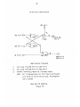
Variables and Flags for MACOD3
Name
Location
Function
00E7
Entry point to PAKI interrupt service
routine.
----
003B
Entry point to PAKI idling loop. All
command executions are initiated from
within this loop.
-
0128
Exit point from PAKI interrupt service
routine. Exit returns to standard register
set and enables interrupts.
----
012C
Exit point from PAKI interrupt service
routine. Exit returns to standard register
set but does not enable interrupts.
PPEND
F944
PPEND=0 then normal command processing
is assumed. PPEND<>0 implies that a
SAVE/RESTORE operation has been requested
by the host. The main command buffer is
allowed to become completely empty before
proceeding.
MSP
F940-1
These two bytes contain the
auxilliary stack pointer where
processor registers and cursor
values are stored by the SAVE
special command.
FF42
Number of command bytes in the main
command buffer waiting to be processed
is stored at this location.
-
Figure 20
This code segment is attached to the standard PAKI
service routine.
interrupt
Special commands are the SAVE and RESTORE
envi ronment functions.
MACOD3 Flowchart
Sheet 1/4
Fi gure 21
MACOD3 Flowchart
Sheet 2/4
Figure 21
MACOD3 Flowchart
Sheet 3/4
Figure 21
MACOD3 Flowchart
Sheet 4/4
Fi gure 21
70
of the 91 operation.
Whenever P2 receives an interrupt, the address of the
next instruction to be executed is pushed onto the processor main stack and
execution vectors to the appropriate interrupt service routine.
The SAVE
routine pops this return address information off the main stack and saves
the return address on the auxilliary stack.
A subsequent RESTORE will
load the program counter with the return address from this auxilliary stack
following
restoration
of
the
other
processor
registers
and
cursors.
Chapter IV
System Software-Utilities and an Experimental Example
A large amount of commercial software is available to the PPOD user.
The hardware and firmware sub-modules described earlier provide experimental flexibility: it is the high level language capability which makes this
flexibility accessable on a rapid turn-around basis. The same criteria.for
hardware selection; modularity, simplicity, reliability, were the basis for
software selection.
CP/M is a widely used operating system for disk supported 8 bit
microprocessors. This operating system is adaptable to a range of hardware
and once customized does not demand user expertise to write code exercising
the full
In addition,
system capability.
since CP/M is extensively
marketed there exists a large number of compatable software utility packages and special purpose 10 drivers. The standard CP/M System includes the
Basic 10 System (BIOS),
a text editor, Dynamic Debugging Tool (DDT),
several assemblers (ASM and RMAC).
Both ASM and RMAC produce executable
code from 8080 assembly language mnemonics.
full line of macro facilities.
and
In addition RMAC supports a
These macro facilities have been used to
implement the Z80 command set through the RMAC 8080 assembler and a Z80
macro library.
RMAC produces relocatable object modules which can sub-
sequently be linked together forming an executable memory image.
used
codes.
for loading,
tracing,
and executing
8080 hexadecimal
DDT is
instruction
Via DDT memory locations and processor registers can be examined
and altered.
Although DDT and RMAC allow relatively convenient assembly language
programming a high level language is generally preferred. In the disk based
PPOD supports a PL/I compiler.
development configuration,
The compiler
accepts PL/I source code and produces relocatable object modules similar to
Through the LINK utility PL/I modules can be
those generated by RMAC.
linked directly to assembly language 10 drivers or interrupt service code.
PL/I was selected as the high level language because it
and bit string manipulations.
allows character
Bit string manipulations are vital when it
is necessary to control specialized hardware from a high level language.
The CP/M
operating
including BASIC,
system
FORTRAN,
not been purchased.
is compatable
with
a number
of
languages
and APL however these high level languages have
To further increase the convenience of high level
programming the VEDIT text editor has been purchased.
VEDIT allows complex
text handling procedures whose effects are immediately visible on the CRT
screen.
It is expected that VEDIT will greatly facilitate the development
and documentation of high level source code.
One problem with the standard PL/I compiler is that the code produced
is not formatted in such a way as to be directly put into EPROM.
The main
difficulty is that PL/I code employs a large language data area (approx.
8k) which is accessed by various PL/I library functions.
In order to pro-
perly execute code generated by the PL/I compiler the 8k language data area
must be initialized to the correct values.
Although the starting address
and extent of the language data area is easily determined the function of
each entry has not been documented and is not so easily determined.
Since
the 8k data area would occupy one quarter of the available EPROM it is not
practical to store the entire data base with every program.
Prof. Antonio
Elias has overcome the difficulty by writing routines to compress the
entire region into.less than 2k bytes.
The program, ANAMEM, does this data
compression. Another program, STAR, recohstructs the entire data base from
the output of ANAMEM. By exploiting the large number of zero entries in the
standard language data base, this data compression technique allows initialization of large areas of RAM without having to store each byte's initial value.
Generally, the compressed data base is stored in EPROM and
STAR is used to reconstruct the full data base at the start of processing
code.
In addition to the ABSOLUTE, CODE,
DATA, and COMMON segments listed
in a program's linking statistics there are two other portions of memory
which must be preserved if reliable operation of the ROMed program is to be
insured.
The first is that occupied by the compressed language data area.
This data must reside at the location expected by the reconstruction
routine, STAR.
The second auxilliary area is the region from 0000-0100
which is used by CP/M for storage of system parameters.
These memory loca-
tions should be programmed into EPROM following a successful load and execution of the program to be ROMed.
Prior load and execution ensures that
the system parameters put in EPROM will be exactly those needed. by the
running program.
It is prudent to alter the system parameters slightly by
programming a RET instruction at the BOOT and BDOS entry points (0000 and
0005).
Programming of EPROMs must be preceded
debugged and properly executing CP/M program.
by creation of a fully
If the program to be placed
in ROM is named 'RMCD'
then the executable menory image will be stored in
the disk file 'RMCD.COM'
following a successful link.
loaded into system RAM via the DDT utility.
cessfully loaded,
The COM file can be
Once the file has been suc-
the processor monitor is reentered by depressing the
system reset button on the mainframe front panel.
This reset operation
terminates any running program but does not reset the system RAM, thus the
executable memory image
operation.
loaded with DDT is not destroyed by the reset
The monitor command 'P <starting address> <end address> F800'
will then program the memory segment <starting address> to <end address>
into the (blank!) EPROM located at F800-FFFF.
Repetition of this process
will place the entire executable memory image in EPROM.
Before execution of the EPROM based program, the P1 memory map must
be reconfigured so there are no address conflicts between RAM and EPROM.
The RAM from E700-FOOO must never be deselected.
by the P1 monitor initialization code.
system RAM and stack
reconfiguration
These locations are used
P1 will not run any code if
space have been overlayed with EPROM.
of the
memory map,
the ROMed
code can be
resetting the system and issuing a 'G <starting address>'
the
Following
invoked by
instruction from
For PL/I code developed under the CP/M operating system
the user consol.
the starting address will be 0100H.
ANAMEM and STAR when combined with standard CP/M utilities allow
the
production
experimental
of
ROM
applications
based
programs
preclude disk
written
drives,
in PL/I.
the
Since most
development
of a
technique for creating ROMed PL/I programs constitutes a vital extension of
the standard system software.
Using the procedure described above a prototype Loran-C based RNAV
Portions of the RNAV processing are done by the PO
has been implemented.
control
program described earlier in connection with the task dependent
The bulk of the data processing is done by PL/I
portion of the IPCP.
routines burned into EPROM.
Elias.
PL/I code for the RNAV was written by Prof. A.
This prototype RNAV has been tested in an automobile.
Loran-C data from this test run is shown in figure 22.
A plot of
Inputs to the PL/I
processing code are derived from two sources; the Loran-C receiver and the
RNAV user keyboard.
Present position is provided from the receiver in
latitude/longitude.
The RNAV user can program a sequence of waypoints to
his destination.
Provision is made for adding, deleting, and inserting
Although the position fix is based
waypoints in a numbered waypoint list.
on Loran-C signals, waypoints are specified relative to the existing VOR
As with conventional RNAVs waypoints can be defined at a named
network.
VOR or at an entered range and bearing from a named VOR.
Use of this
'pseudo VOR'
attractions.
approach to defining
waypoints
has
several
Pilots are familiar with the existing YOR network and rho/theta navigation.
The VORs and connecting radials appear on air route charts and the VOR
geographic positions can easily be stored in EPROM.
are stored in EPROM,
accessable
without
Once the VOR positions
the excellent accuracy of the Loran-C network is
the
inconvenience
of
time
difference
coordinates.
Waypoints can be defined simply by entering a VOR name, radial,
through the command entry keyboard.
and offset
The entire operator command set for
entering, deleting, and changing waypoints is given in figure 23.
Calculations involving geographic coordinates are done assuming a
spherical earth; however, a series of linearized correction factors are
Mobile Test Run Data Plot
Unfiltered Loran-C Data
-1n
1nm.
Figure 22
Comand Code
Effect.
Format
G, 10
T
Set CDI gain to 10
Current course is toward
Waypoint
Current course is from
Waypoint
R 1 110
D
Set desired radial to 110
Delete waypo'int shown
S n
Show name, radial, offset of nth waypoint
A n
Navigate toward nth
Waypoint
Navigate toward previous
Waypoint
E 1 BOS
Define BOS VOR as firstWaypoint
Insert waypoint before
Waypoint shown
I1
Error Messages
INSUFFICIENT DATA-
Command string too short.
INCORRECT DATA-
Alpha/numeric expected in place of
numeric/alpha in command string.
WP NOT DEFINED-
User has tried to navigate to a waypoint which has not yet been entered
via the E 'comm'and.
NAMED WP NOT FOUND-
User has tried to define a waypoint
not contained in the system waypoint
data base.
INTERNAL CONVERSION ERROR-
Overflow/underflow in software
arithmetic function.
RNAV program commands and error ressages
Figure 23
used to account for the deviation in bearing angle with longitude.
The
correction factors are computed preflight and are entered directly into the
program at compile time.
The equations used for computation of position
relative to a desired course are given in figure 24 and are based on those
given in Ref 8.
The magnitude of error incurred by the spherical earth
approximation is well within acceptable limits for enroute navigation at up
to 500 nm ranges.
These approximations would not in general be acceptable
for non-precision approach flying.
A sample RNAV output CRT image is shown in the succeeding figure.
In addition to the CDI arrow near the center of the screen there are three
regions of interest.
top of the screen.
ground speed,
The first is the active waypoint display shown at the
This region indicates the name, number, course, radial,
and time to go relative to the waypoint whose position is
used in the cross-track deviation calculation (the active waypoint).
At
the lower most edge of the screen is the area used for command and error
message display.
Immediately above the command/error message display is
the temporary waypoint display region.
This portion of the screen is used
for review of previously defined waypoints and the display of other temporary command/status data.
The active waypoint display is independent of
the content of the temporary waypoint display.
directly
alter
the
contents
of
the
Only the 'A',
active
'B' comands
waypoint
region.
Arc-length and Bearing Calculations
Under the assurption of a spherical earth the follcwing
equations can be used to co-pute the arc distance and bearing
frm north of two points, A and B, with kncwn latitude and
longitude.
A AA
are latitude/longitie of point A
B' AB
are latitude/longitude of point B
AA =AA AB
9= cosB* sin A
C
osA*
s2= sin-B sinA* cos 4IB* co-sA
- 3= sin"A * sintB + coslA* cos@ * c)A
Angle of the arc from A to B rreasured from true North is
-t=t~1
(C 22
Arc-length from A to B is given by
p = a{tan ~ ((C 2 os
+C1 sin* )/C 3
a= 3443 nm.
Navigation Equations for RNAV Program
Figure 24
V
M
I
N
Q
U
M
.5
(CDI error markings)
(CDI arrow)
(CDI centerline)
WPNT DISPLAY:
WP#V9
OFF
--OFFSET-DIST
BRNG
DES.RAD,
(waypoint entry/review area)
ENTER COMMAND:
(command entry and error message display)
RNAV p:9rAm CRT Display
riure 25
Chapter V
Conclusions and Recommendations for Continued Research
The previous chapters have covered the existing PPOD system from
hardware, firmware, and software perspectives.
very diverse set of experimental
laboratory.
Clearly PPOD can support a
objectives both airborne and in the
Because of PPOD's versatility any comprehensive listing of
future objectives would be nothing more than a hinderance to future users;
rather I shall list a few areas of immediate interest some of which have
served as the seeds from which the PPOD project sprang and some of which
have grown out of the systems integration and development effort.
The PPOD project development effort has achieved several important
results.
A simple but nevertheless crucial task was the selection of the
stock electronic boards on which the system is based.
of
manufacturers
offerring
various
combinations
From the large array
of
features
it was
necessary to chose three or four whose products could form a substrate upon
which further enhancements would be based.
The wide range of possible
applications for the PPOD multiprocessor is an indication of success in
meeting this requirement.
Initial component selection and purchase was
followed by a series of enhancement modifications.
These enhancements
include addition of Z80 mode 1 interrupt support to the PO processor, the
creation of circuitry
and firmware to allow interrupt driven communication
between the P1 and P2 processors, and perhaps most important the addition
of the electronics and the graphics operating system extension required to
nultiplex several
video data sources onto a single CRT.
modifications has been successfully implemented
Each of these
as an extension to the
capabilities of the equipment as originally purchased.
Another objective
of the process of integrating the stock components was to make the functional extensions mentioned above without impacting the performance of the
electronic submodules when operated in more conventional applications.
every case this objective has been met.
In
None of the hardware/firmware
modifications described in preceding chapters detracts from the operation
of the units when operated in the manner intended by the manufacturer.
The capabilities of the PPOD system have been verified in a mobile
environment through an automobile test run.
This test involved observation
of the performance of a prototype Loran-C based RNAV with CRT display.
Addition of a latched 8/16 bit multiplexor circuit to the Loran-C receiver
data bus provided a convenient method of taking position information from a
Northstar 6000 receiver and the multiplexor also eliminated interference
between the PPOD and receiver digital
data buses.
An assembly language
program run by the PO microprocessor controlled the multiplexing and processing of receiver data.
Following coordinate conversion calculations a
CRT image providing destination, cross-track error, and groundspeed information was displayed to the operator.
recorded
for
later
analysis.
Loran-C position data was also
Successful
implementation
of the RNAV
demonstrates the power of a multiprocessor configuration, the convenience
of high level language capability, and the ease with which PL/I code can be
linked to hardware dependent utility routines.
From the results achieved a number of general conclusions can be
drawn.
Experience to date with the Loran-C based RNAV and CRT display
indicates
that the
inconvenience
of time
difference coordinates and
hyperbolic grid navigation can be shifted to a digital processing system
with moderate intelligence.
Once these details are
computer,
system will cause no increase in pilot
use of the Loran-C
relegated to a
workload as compared to a conventional RNAV system. Use of the PPOD system
has demonstrated that 'off the shelf' electronics can be used to achieve a
variety of experimental objectives both in the air and on the ground.
Detailed knowledge of the internal stiucture of the standard components can
be used to integrate several modules into a multiprocessor.
In addition
the PPOD development effort has shown that some of the advantages of
multiprocessing can be achieved with ordinary equipment and carefully
engineered interface modifications.
Throughput increases- are available
without the necessity of formulating the experimental task in terms of many
subtasks, an execution lattice, and a multiprocessor executive.
Most
of
the immediate
peripheral equipment.
needs
relate
to
improvements
in the
A high resolution direct drive CRT of standard
instrument bay size would ease the logistics of flight testing. The rather
awkwardly packaged unit in use does not allow mounting close to other
critical flight instruments.
small
key array,
contribute
simulations.
A similar need exists on the input side.
perhaps kneepad or instrument panel
mounted,
A
would
greatly to flight tests and add to the realism of ground
PPOD's multiprocessor organization and multiple memory maps
provide a solid platform for experiments with voice input/output.
This is
-
an area which has not been extensively researched and may provide some
relief for the already crowded visual data channels.
compatable
voice synthesis
modification.
board would
A simple voice feedback
Addition of an S-100
not require extensive
for keyboard
software
input would allow
pilots to enter command/request data while looking at flight instruments.
Simulation flight testing offers unique opportunities and savings in cost.
Before extensive simulation testing can be done,
improvements will have to
be made in the analog/digital converters presently available.
Preliminary
work has indicated that the conversion spe.ed and resolution of the 12 bit
A/D units now installed in the PDP-11/10 computer are not adequate for producing a stable display driven by analog simulator outputs
[Ref.
7].
Reduction in conversion granularity especially would improve the usefulness
of the simulator/PPOD/PDP-11 combination.
Great possibilites exist for the coupling of a digital autopilot
Experiments involving RNAVs based on various raw data sources
with PPOD.
are only a few of the opportunities.
Implementation of weight, balance,
and range optimization calculations do not require any additional hardware.
A series of qualitative workload studies would be the next logical step
following implementation of an electronic copilot of the type described
earlier.
These are some of the possible experiments as outlined under the
three test levels described in chapter 1.
effort
has
been
devoted
to
definition
To date most of the research
of
the
implementation of a prototype Loran-C based RNAV.
PPOD
architecture
and
The computational power
and mission flexibility of the PPOD multiprocessor should in the future be
utilized at all three of the experimental levels of chapter 1.
The current pace of hardware development makes is difficult even
for rapidly moving production operations to keep abreast of the latest
innovations.
In the space of a year most of the digital circuit boards
used in PPOD have been obsoleted by new models and board revisions.
spite of this fact,
tool.
PPOD
PPOD will
interfaces
with
In
retain its utility as an experimental
much
of
the older
equipment
and
its
components will be compatable with the S-100 equipment of the next several
years.
System architecture provides for modular upgrade as well.
Although designed to fulfill the general requirements of the three
test levels described in chapter 1, already PPOD's versatility has led to
unanticipated applications.
Two examples are use as a microprocessor
development system for remote manipulator firmware simulation/design and as
a development environment for a microprocessor based airline scheduling
system.
There is little doubt that PPOD multiprocessor versatility will
continue
to
be
utilized
in a range
of
imaginative test
programs.
References
1.
Sheridan, T.B., Ferrel, W.B., Man-Manchine Systems:
Information, Control, and Decision Models of Human
Performance, MIT Press, Cambridge MA, London England,
1974
2.
Hess, R.H.; Structural Model of Adaptive Human Pilots,
Journal of Guidance and Control, vol. II No. 5, 1980
3.
Cornsweet, T.N., Visual Psychophysics, Academic Press
New York NY, 1970
4.
Graham, C.H. ed., Vision and Visual Perception,
Wiley, NY, 1965
5.
Green, Swets, Signal Detection Theory and Psychophysics,
Wiley, NY, 1966
6.
Kelley, D.H., Visual Contrast Sensitivity, Optica Acta,
vol 24 No. 2, 1977
7.
Cohen, J.C., Evaluation of Alternative Instrument Landing
System Displays, 16.622 Experimental Projects IReport,
MIT Dept. Aeronautics and Astronautics, 1981 -
8.
Kayton, M., Fraid, W., ed., Avionics Navigation Systems,
John Viley ad Sons Inc., New York, London, Sydney, Toronto, 1969
Bibliography
Data Link Airborne
Lincoln Laboratory,
1.
Anderson, J.C., Leeper, J.L., The DABS
Intelligent Display Operator's Manual, MIT
Bedford MA, 1980.
2.
Barden,
Howard W. Sams & Co.
3.
Single Pilot IFR Autopilot Complexity/
Bergeron, H.P.,
Benefit Tradeoff Study, Flight Dynamics and Control Division,
NASA Langley Research Center, Harpton VA, AIAA paper 80-1869, 1980
4.
Bulloch, C., The Speaking Computer: Automatic Voice Advisory Systems
Coming On Line, Interavia Vol. 12i 1980
5.
Bunker, W.M., Ingalls, Capt. M.L., Circles, Texture, Etc.;
Alternate Approaches to CIG Scene Detail, AIAA Flight, Simulation
Technologies Conference paper #49, 1978
6.
California Computer Systems, Model 2200 Mainframe
Manual, California Computer Systems, Sunnyvale CA, 1980
7.
Cessna Aircraft Co., Cessna Skylane Model 1820 Information Manual,
Cessna Aircraft Co., Wichita, Kansas, 1978
8.
Chang, E.T., A VTOL Prediction Display,
Dept. Aeronautics and Astronautics, 1969
9.
Chang, E.T., Evaluation of Elements In a Contact Analog Display,
SM Thesis, MIT Cambridge MA, 1970
10.
in Avionics,
Advances
G.W.,
Church,
Ft. Lauderdale FL., AIAA paper 79-0562, 1979
11.
Hardy,
Berkstresser,
Callas,
Jackson,
Denery,
Aircraft,
Aviation
General
Future
for
Avionics
Integrated
NASA Ames Research Center, AIAA paper 78-1482, 1978
12.
Introduction to CP/M Features
Digital Research, An
Facilities, Digital Research, Pacific Grove CA, 1976, 1977, 1978
13.
Digital Research, CP/M Assembler User's Guide,
Pacific Grove CA, 1976, 1978
14.
Digital Research, CP/M
Research,
Digital
Handbook,
Microcomputer
Z-80
The
W.,
Inc., Indianapolis, Ind., 1978
Engineer's
Owner's
Thesis, MIT
Bendix
Corp.
and
Digital Research,
Dynamic Debugginq Tool (DDT) User's Guide,
1978
1976,
CA,
Grove
Pacific
15.
Digital Research, CP/M MAC Macro Assembler:
Languaae Manual and
Applications Guide, Digital Research, Pacific Grove CA, 1976, 1978
16.
Digital Research, ED:
A Context Editor for the CP/M Disk System
User's Manual, Digital Research, Pacific Grove CA, 1976, 1978
17.
Ditital Research, Link-80
Pacific Grove CA, 1980
Operators
18.
Digital Research, PL/I-80
Pacific Grove CA, 1980
Language
19.
Digital Research Computers, 32K S-100 EPROM Card
Specification, Digital Research Computers, Garland TX, 1980
20.
Electonics Division,
Electronics Research and
for Civil Aviation, Electronics Division of the
of Electrical Engineers, Savoy Place, London, 1963
21.
Eskenazi,
R.,
Williams, D.S.,
Modular On-board
Imaging, JPL Pasadena CA, AIAA paper 7801715,'1978
Adaptive
22.
Freuler, R.J.,
Hoffman, M.J.,
Experiences with an
Digital Computer System for General Aviation Flight
Ohio State University, AIAA paper 79-1834, 1979
Airborne
Testing,
23.
Green, T., VEDIT, A Visual Editor User's
Products, Inc., Ann Arbor, Michigan, 1980, 1981
24.
Honeywell, Demonstration Advanced Avionics System, Function
Description,
Honeywell
Avionics
Division,
Minn.
Minnesota,
King Radio Corp., Kansas, 1980
25.
Imrich, T.,
Concept Development
Traffic
Displays,
MIT
Flight
report R77-2, Cambridge MA, 1971
26.
Kayton, M.,
Freid, W.,
ed.,
Avionics Navigation Systems,
John Wiley and Sons, Inc., New York, London, Sydney, Toronto, 1969
27.
Kirkpatrick, G.M., Real Time Weather Display
Aviation
Cockpit,
CMK
Consulting
Services,
AIAA Paper 79-1821, 1979
28.
LaRusso, J.A., Gill, A.T., Optical Stimulator with Holographic
Component,
AIAA
Flight
Simulation
Technologi es
Conf.-1978,
paper 176, 1978
29.
McGlynn,
H.J.
Jr.,
Collins,
J.W.F.,
Microprocessor
Digital
Control,
GE
Co.,
Lynn MA, AIAA paper 80-1149, 1980
Guide,
Manual,
Digital
Research,
Digital
Research,
Development
Institution
Manual,
and Evaluation
Transportation
Product
of
ConpuView
Airborne
Laboratory
in the General
Syracuse
NY,
Full
Authority
Binghamton
NY.
30.
Measurement Systems and ,Controls, Technical Manual, DM6400
Series S-100 Dynamic Merory Boards, Measurement Systems and
Controls Inc., Orapge CA, 1979
31.
Miller, G.K. Jr., Riley, D.R., The Effect of Visual-Motion
Time Delays on Pilot Performance in a Pursuit Tracking Task,
AIAA Visual andMotion SimulationCornf., 1976
32.
NASA, Avionics: Projections for Civil Aviation, 1995-2000,
Report CR-159035, NASA Langley Research Center, Hampton VA, 1978
33.
Pal mer, E., Petitt, J., Visual Space Perception on a Computer
and Motion
AIAA Visual
Attachment,
Graphics_ Night Visual
Simul ation Conference, 1976
34.
System - A New
The 767's Flight-Management
R.A.,
Peal,
Generation of Airborne Avionics, Astronautics and Aeronautics,
vol. 18 No. 11, 1980
35.
Poole, H.H., Fundamentals
Ltd., London, 1966
36.
Purser, K., Interactive Computer Graphics, Boeing
Airplane Co., Seattle WA, AIAA paper 80-1889, 1980
37.
Reike, R.R., Compu-Scene- Modular Approach to Day-Night Computer
Image Simulation, AIA Visual and Motion Simulation Conf., 1976
38.
G.J.,
Sutty,
Jr.,
W.0.
Duncan,
R.V.,
Reynolds,
Scenes,
Textured
Via
Cues
Motion
and
Perception
Depth
AIAA Flight Simulation Technologies Conf.-1978,
paper 46, 1978
39.
Corp.,
Scion
Vienna VA, 1980
40.
Spracklen, K., Z-80 and 8080 Assembly
Haydn Book Co., Inc., Rochelle Park, NJ, 1979
41.
Motion Perception and
Stark, E.A.,
Simulation, AIAA Visual
Air Combat
Conf., 1976
42.
Swall ow, R., Goodwin, R., Draudin, R., Computrol - A New
Technique in Image Generation, AIAA Flight Simulation Technologies
Conf. -1978, paper 59, 1978
43.
Teletek,
1980
44.
Intelligent
Teletek,
Teletek, Sacramento CA, 1980
FDC-1
of Display Systems,
MicroAngelo
Product
MacMillan and Co.
Scion
Manual,
User's
Commercial
Language
Corp.,
Programming,
Terrain Visual Cues in
Simulation
Motion
and
Specification,
Teletek,
Sacramento CA,
Interface
Product
Specification,
90
45.
Texas Instruments, The TTL Data
Texas Instruments Incorporated, 1976
46.
Wu, C., A Digital System to Produce
JPL Pasadena CA, AIAA paper 76-968, 1976
47.
Young, L., Research on Integration of Visual and Motion Cues
for
Flight
Simulation,
Manned
Vehicle
Laboratory,
MIT
NASA report CR-153249
48.
Zaks, R.,
CA, 1980
The CP/M
Handbook
with
Book
for
Design
Imagery
MP/M,
Sybex
from
Inc.,
Engineers,
SAR
Data,
Berkeley
Appendix A
Software Listings--Source listings for programs described in the body of the
paper are provided in this appendix.
ISUER5 is a revision of the Northstar 6000 10 control program
IUSER3. This proqram controls the acquisition, error checking, and
formatting of the Loran-C data.
;IUSER4 IS A RELOCATABLE VERSION OF IUSER5
;IUSER5 IS ASSMBLD RELATIVE TO 29A SINCE IT WILL
;BE PLACED AT THAT ADDRESS WHEN MERGED-WITH THE
;STANDARD 1^2 OPERATING CODE, basker.
;REVISION FOR INTERFACE TO PL/1 LORAN CODE.
;DECODES ONLY GPIA DATA AND SENDS AN INTERRUPT TO
;HOST AFTER EVERY 1-2 TO HOST DATA XFER. INTERRUPT VECTOR IS PIOV
;STATWD BIT DEFINITIONS
BIT 0: H-GPIA FRAME IN PROGRESS
BIT 1: RFU
BIT 2: H-GPIA FRAME READY FOR' XMIT
BIT 3: H-SNRS OK ON S1 AND S2
BIT 4: H-EPSCO FRAME IN PROGRESS
BIT 5: RFU
BIT 6: H-EPSCO FRAME READY FOR XMIT
BIT 7: RFU
;CONWD BIT DEFINITIONS
BIT 0= H-DECODE GPIA
BIT 1= H-DECODE.EPSCO
BIT 2= H-DECODE BEST SOURCE
;SNRWD BIT DEFINITIONS
BIT 0= H-CHECK SNR ON NEXT BYTE
BIT 1= H-LAST SNR OK
BIT 2= H-LAST SNR OK
ORG 029AH
ICON
COMSTA
ADR1
PIOV
GPIA
EPSCO
ETAG
GTAG
SNRTHR
IRAM
MOVER
EQU
EQU
EQU
EQU
EQU
EQU
EQU
EQU
EQU
EQU
EQU'
03000H
05000H
OBOOOH
OF8H
020H
010H
O1H
02H
04H
01000H
0151H
INTVCT
DMADDR
WTFLG
MAXL
BOTM
GADDR
EQU
EQU
EOU
EQU
EQU
EQU
023BFH
023B8H
023B5H
060H
01200H
BOTM+1
;I^2/HOST STATUS PORT
;HOST PIO INT VECTOR
;GPIA FRAME ID BITS
;EPSCO FRAME ID BITS
;GPIA FRAME ID TAG
;EPSCO FRAME ID TAG
;SNR LEVEL THRESHOLD
;BASE OF TRANSMIT BUFFER
;ADDRESS OF DMA TRANSFER ROUTINE
;IN 1^2 BASIC KERNEL
;HOST INT VECTOR STORAGE LOCATION
;DMA ADDRESS STORAGE LOCATION
;DMA DIRECTION CONTROL BYTE LOC.
;MAX RING BUFFER LENGTH
;BASE OF PROGRAM SCRATCH RAM
EADDR
INLOW
INHGH
CONWD
SNRWD
GBASE
EBASE
BASR
SCRAT1
BTG02
EQU
EQU
EQU
EQU
EQU
EQU
EQU
EQU
EQU
EQU
GADDR+1
EADDR+1
INLOW+1
INHGH+1
CONWD+1
SNRWD+1
GBASE+28
EBASE+13
BASR+96
SCRAT1+2
OBASE1
OBASE2
STATWD
EQU
EQU
EQU
GBASE
EBASE
BTG02+1
JMP SUPR
INTSEV: PUSH PSW
OK6:
LCHK2:
OVE2:
MVI A,082H
STA 08001H
LDA 08000H
DB
ODDH,077H,00
ANI 070H
JZ OK6
DB
OCBH,6*8+A+4 OH
JNZ OK6
LDA BTG02
CPI MAXL
DB
ODDH,23H
CALL LCHK2
MVI A,081H
STA 08001H
LDA 08000H
DB
ODDH,077HOO
DB
ODDH,23H
CALL LCHK2
POP -PSW
El
RETI
DB
OEDH,4DH
LDA BTG02
INR A
STA BTG02
DB
ODDH,22H
DW
SCRAT1
LDA SCRAT1
CPI MAXL
JC OVE2
DB
ODDH,21H
DW
BASR
RET
;TEMP. STORAGE FOR LOW BYTE INPUT
;TEMP. STORAGE FOR HIGH BYTE INPUT
;LOCATION OF CONWD
;LOCATION OF SNRWD
;GPIA FRAME BUFFER BASE ADDR.
;EPSCO FRAME BUFFER BASE ADDR.
;RING BUFFER BASE ADDRESS
;SCRATCH PAD RAM LOCATION
;CONTAINS # OF BYTES IN RING
;BUFFER WAITING FOR PROCESSING
;STATWD LOCATION
;JMP TO INITIALIZATION CODE
;START OF NORTHSTAR 6000 INT
;SERVICE ROUTINE
;ENABLE HIGH ORDER BYTE
;READ HIGH ORDER BYTE
;CHECK ADDRESS BITS FOR GPIA,EPSCO
;IF WRONG DEVICE THEN QUIT
;CHECK TO SEE IF RING BUFF IS FULL
;CHECK BUFFER LENGTH
;ENABLE LOW ORDER BYTE
;READ LOW ORDER BYTE
;SAVE LOW ORDER BYTE
;RETURN FROM INTERRUPT
;INCR # OF BYTES IN RING BUFFER
;LOAD SCRATI INTO IX
;PUT BYTE INTO RING BUFFER
;ROUTINE PROCESSES BYTES FROM THE RING BUFFER AND ACCUMULATES DATA
;FRAMES IN SPECIAL BUFFERS RESERVED FOR EACH TYPE OF DATA FRAME
EXINT:
PUSH PSW
PUSH H
PUSH B
CALL GETBT
STA INHGH
CALL GETBT
STA INLOW
MVI AGPIA
MOV B,A
LDA INHGH
ANA B
CNZ GPROC
MVI A,EPSCO
MOV B,A
LDA INHGH
ANA B
CNZ EPROC
POP B
POP H
POP PSW
RET
;GET A BYTE FROM THE RING BUFFER
;GET A BYTE FROM THE RING BUFF.
;SAVE IN A TEMPORARY LOCATION
;GET THE LOW BYTE FROM RING BUFF.
;SAVE IN A TEMPORARY LOCATION
;CHECK ADDRESS BIT TO SEE IF IT
;IS PART OF A GPIA FRAME
;IF NOT GPIA THEN CHECK TO SEE
;IF IT IS PART OF AN EPSCO FRAME
;GO TO EPSCO PROCESSING CODE
- -
;RETURNS WITH A BYTE FROM THE RING BUFFER IN THE "A" REGISTER
GETBT:
OVE3:
DB
OFDH,O7EHOO
PUSH PSW
OFDH,23H
DB
OFDH,22H
DB
SCRAT1
DW
LDA SCRATI
CPI MAXL
JC OVE3
OFDH,21H
DB
BASR
DW
LDA BTG02
DCR A
STA BTG02
POP PSW
RET
;PROCESS GPIA DATA
GPROC:
PUSH PSW
PUSH H
PUSH D
LDA INHGH
RRC
JNC NST
;DECREMENT BYTES LEFT IN BUFF.
NST:
LCHK:
RRC
J NC
RRC
JNC
RRC
JNC
iMP
LDA
DB
C NZ
POP
POP
POP
RET
NST
NST
NST
LCHK
STATWD
OCBH,O*8+A+40H
SAVE
D
H
PSW
LDA GADDR
;START OF FRAME MARKED BY 'OF' BYTE
;IF START OF FRAME GOTO LCHK
;IS A FRAME BEING ACCUMULATED?
;YES-THEN SAVE THE BYTE
;NO- THEN EXIT WITHOUT SAVE
;HAS A PREVIOUS FRAME BEEN FILLED?
CPI 01BH
CZ MVE
CALL RESYNC
CALL SAVE
POP D
POP H
POP PSW
RET
RESYNC: LDA
DB
STA
XRA
STA
RET
MVE:
STATWD
OCRH,0*8+A+OCOH
STATWD
A
GADDR
LDA STATWD
DB
OCBH,2*8+A+OCOH
DB
OCBH,O*8+A+OCOH
STA STATWD
RET
;IF YES THEN SET FRAME COMPLETE FLAG
;IF NO THEN START A NEW FRAME
;SAVE FIRST BYTE IN NEW FRAME
;SET STATUS TO INDICATE THAT A
;GPIA FRAME IS BEING ACCUMULATED
;SET GPIA BUFFER POINTER TO BOTTOM
;OF GPIA BUFFER
;SET STATUS TO INDICATE THAT A FULL
;FRAME IS READY TO BE SENT TO HOST
;STORE A BYTE IN GPIA BUFFER
SAVE:
LXI H,GBASE
LDA GADDR
MOV E,A
INR A
STA GADDR
XRA A
MOV D,A
DAD D
LDA INLOW
MOV M,A
CALL SNRCHK
RET
;PUT BASE ADDRESS OF GPIA BUFF IN 'HL'
;GET OFFSET FROM BASE FOR NEXT
;EMPTY LOCATION.
;SAVE BYTE IN EMPTY LOCATION
;CHECK SNR LEVEL
;PROCESS EPSCO DATA
EPROC:
PUSH PSW
PUSH H
PUSH D
LDA INHGH
ANI OFH
JZ ECHK
LDA
DB
CNZ
POP
POP
POP
RET
STATWD
OCBH,4*8+A+40H
SAVE2
D
H
PSW
;LOOK FOR START OF EPSCO FRAME
;IS EPSCO FRAME ALREADY BEING
;ACCUMULATED?
;YES-SAVE BYTE
;NO EXIT
;CHECK FOR START OF FRAME
ECHK:
LDA STATWD
OB
OCBH,4*8+A+OCOH
STA STATWD
LDA EADDR
CPI OCH
CZ MVE2
XRA A
STA EADDR
POP D
POP H
POP PSW
RET
;SET STATUS TO INDICATE THAT AN
;EPSCO FRAME IS BEING ACCUMULATED.
;IS A PREVIOUS FRAME FULL OR
;IS THIS THE FIRST ONE.
;IF NOT FIRST ONE THEN SEND-FULL
;FRAME TO HOST AND SET BUFFER
;POINTER TO BOTTOM OF BUFFER
;MOVE EPSCO BUFFER
MVE2:
LDA STATWD
DB
OCBH,6*8+A+OCOH
STA STATWD
RET
;SET EPSCO FRAME FULL STATUS
;SAVE EPSCO DATA BYTES
SAVE2:
LDA
ANI
CPI
RZ
ORA
RZ
LXI
LDA
MOV
INR
STA
MVI
DAD
INHGH
07H
07H
A
H,EBASE
EADDR
E,A
A
EADDR
DOOH
D
;IS IT AN EPSCO DATA WORD
;YES BUT IT IS A LOAD
;COMMAND SO DONT SAVE IT
;IT IS A RESET COMMAND,
;DONT SAVE IT
;PUT EPSCO BUFF. BASE IN 'HL'
;ADD OFFSET TO BASE
LDA INLOW
MOV M,A
RET
;PUT BYTE IN FREE LOC.
;ROUTINE TO CHECK SNR LIMITS
SNRCHK: LDA GADDR
CPI 017H
CZ DCHK
LDA GADDR
CPI 018H
CZ SNRC
RET
DCHK:
LDA INHGH
ANI 07H
CPI 02H
JZ SKP
CPI 03H
SKP:
EXT5:
SNRC:
OK1:
LSNR:
JNZ
LDA
DB
STA
RET
LDA
DB
STA
RET
EXT5
SNRWD
OCBH,0*8+A+OCOH
SNRWD
;SNR DATA WILL BE IN BYTES 23,24
;IS IT BYTE 23?
;IS IT BYTE 24?
;BYTE 23 INDICATES THE SLAVE #
;FOR SNR DATA IN BYTE 24
;IS IT DATA FOR SLAVE #1
;OR SLAVE #2
;IF FOR #1,#2 THEN SET STATUS
;SO NEXT BYTE WILL BE CHECKED
;AGAINST THE SNR THRESHOLD
SNRWD
OCBH,0*8+A+80H
SNRWD
LDA SNRWD
DB
OCBH,O*8+A+40H
JZ EXT5
LDA INLOW
CPI SNRTHR
JM LSNR
LDA SNRWD
DB
OCBH,1*8+A+40H
JZ OK1
DB
OCBH,2*8+A+OCOH
DB
OCBH,1*8+A+OCOH
DB
OCBHO*8+A+80H
STA SNRWD
RET
LDA SNRWD
DB
OCBH,1*8+A+80H
DB
OCBH,0*8+A+80H
DB
OCBH,2*8+A+80H
STA SNRWD
RET
;COMPARE SNR VALUE AGAINST SNR THRESH
;IF SNR TOO LOW THEN JMP TO LSNR
;OTHERWISE SET AN SNR OK FLAG
;IF SNR TOO LOW THEN RESET THE
;SNR-OK FLAGS
;SUPERVISOR ROUTINE
;-FOLLOWING THE INITIALIZATION PROCEDURE AN IDLING LOOP IS ENTERED
;-THIS LOOP SCANS THE RING BUFFER AND PROCESSES THE INCOMING BYTES
;-AS THEY ACCUMULATE IN THE RING BUFFER. WHENEVER A COMPLETE DATA
;-FRAME, EPSCO OR GPIA, IS READY AN ATTEMPT IS MADE TO TRANSFER THE
;-DATA TO THE HOST PROCESSOR AT THE DMA TARGET ADDRESS
SUPR:
PUSH PSW
PUSH H
XRA A
STA SNRWD
STA EADDR
STA GADDR
STA STATWD
STA INTVCT
STA GADDR
STA EADDR
STA SNRWD
STA STATWD
STA BTG02
MVI A,01H
STA CONWD
MVI A,083H
STA 08001H
LXI HADR1
SHLD 023B8H
MVI A,PIOV
STA INTVCT
DDDH,21H
DB
DW BASR
DB
OFDH,21H
BASR
DW
;DISABLE 1^2 TO FDC-1 INTS
;ENABLE GPIA DECODING
;DISABLE OUTPUT ON DPTL
;SET DMA TARGET ADDRESS TO ADR1
;1^2 WILL RETURN PIOV DURING HOST INT
;ACKNOWLEDGE CYCLE IF PIOV<0
;INITIALIZE RING BUFFER POINTERS
;ENABLE MODE 1 INTERRUPTS
SUPR1:
DB
OEDH,56H
DB
EI
POP H
POP PSW
LDA STATWD
OCBH,2*8+A+40H
CNZ XGP
LDA STATWD
OCBH,6*8+A+40H
DB
CNZ XEP
LDA BTG02
ORA A
CNZ EXINT
JMP SUPR1
;IS A GPIA FRAME READY?
;IF YES THEN TRY TO SEND IT
;IS AN EPSCO FRAME READY?
;IF YES THEN TRY TO SEND IT
;ARE BYTES WAITING IN RING BUFF?
;YES-GO TO PROCESSING ROUTINE
;LOOP BACK TO IDLING LOOP
;CODE TO PROCESS A GPIA DATA FRAME
XGP:
LDA CONWD
OCBH,0*8+A+40H
DB
CNZ SEGP
;DOES HOST WANT GPIA FRAMES?
;YES TRY TO SEND
SEGP:
LDA CONWD
DB
OCBH,2*8+A+40H
CNZ BSRCE
LDA STATWD
DB
OCBH,2*8+A+80H
STA STATWD
RET
XRA A
DCR A
STA WTFLG
LXI B,01H
CALL MOVER
LDA IRAM
ORA A
RNZ
LXI H,IRAM
MVI A,GTAG
MOV M,A
LXI B,01CH
LXI HOBASE1
LXI D,IRAM+1
DB
OEDH,OBOH
XRA A
STA WTFLG
LXI B,01CH
CALL MOVER
CALL OPCOM
RET
;MAYBE-IS GPIA THE BEST SOURCE?
;ALTER BUFFER STATUS FLAGS
;SET WTFLG FOR HOST->I^2 TRANSFER
;GET IST BYTE FROM FDC-1 DATA BUFF
;IS FIRST BYTE =0?
;IF NOT THEN HOST IS STILL USING
;LAST FRAME
;SET WTFLG FOR XFER TO HOST
;SET UP FOR XFER TO FDC-1, 'lC' BYTES
;CALL ROUTINE TO DO DMA
;CALL ROUTINE TO GENERATE INT TO HOST
;BSRCE DETERMINES WHICH OF THE TWO FRAMES, GPIA OR EPSCO, IS PREFERRED
BSRCE:
SEGP2:
LDA SNRWD
DB
OCBH,1*8+A+40H
JZ SEGP2
DB
OCBH,2*8+A+40H
RNZ
CALL SEGP
RET
;WERE SNRS ABOVE THRESHOLD
;ON FIRST AND SECOND SLAVES?
;IF NOT THEN SEND GPIA FRAME
;CALL ROUTINE TO SEND GPIA DATA
;CODE TO SEND AN EPSCO DATA FRAME
XEP:
LDA
DB
CNZ
LDA
DB
CNZ
LDA
DB
STA
RET
BSRCE2: LDA
DB
;IS EPSCO DATA WANTED?
CON
OCBH,1*8+A+40H
SEP(
CONtWD
OCBH ,2*8+A+40H
BSR(CE2
STA TWD
OCBH,6*8+A+80H
STAlTWD
SNRW D
OCBH ,1*8+A+40H
;IF YES THEN TRY TO TRANSFER
;IS PREFERRED SOURCE WANTED?
;ALTER BUFFER STATUS.
;WERE LAST TWO SNRS ABOVE THRESHOLD?
100
RZ
DB
OCBH,2*8+A+40H
RZ
CALL SEPC
RET
;RETURN IF NOT
;RETURN IF NOT
;IF BOTH OK THEN SEND EPSCO DATA
;CODE TO SEND EPSCO DATA FRAMES TO HOST PROCESSOR
SEPC:
XRA A
DCR A
;SET WTFLG FOR XFER FROM HOST
STA WTFLG
;GET ONE BYTE FROM HOST MEMORY
LXI B,01H
;IF FRST BYTE=O THEN THE DATA IS USED
CALL MOVER
LDA IRAM
ORA A
RNZ
LXI H,IRAM
;ATTACH EPSCO TAG TO FRAME
MVI A,ETAG
MOV M,A
;OK, SEND 'D' MORE BYTES TO HOST
LXI B,ODH
LXI H,OBASE2
;MOVE FROM TEMPORARY BUFF. TO 10 BUFF.
LXI D,IRAM+1
DB
OEDH ,OBOH
XRA A
STA WTFLG
;SET WTFLG FOR XFER TO HOST MEMORY
LXI B,0DH
;'D' BYTES TO XFER
CALL MOVER
;CALL ROUTINE TO DO DMA
CALL OPCOM
;CALL ROUTINE TO GENERATE HOST INT.
RET
;ROUTINE TO GENERATE INTERRUPTS TO HOST
OPCOM: PUSH PSW
PUSH H
LXI H,ICON
LDA INTVCT
ORA A
JZ GONE
;IF INT VECTOR ZERO THEN LEAVE
LDA INTVCT
STA COMSTA
;PUT INT VECTOR IN OUTBND DATA LATCH
MOV A,M
OPCo:
DB
OCBH ,3*8+A+40H
JNZ OPCO
;WAIT FOR IEI
MVI A,010H
;INTERRUPT HOST
MOV M,A
MOV A,M
OPCl:
OCBH ,1*8+A+40H
;WAIT FOR HOST TO AKNOWLEDGE INT
DB
JZ OPCl
XRA A
;CLEAR INTERRUPT TO HOST
MOV M,A
POP H
GONE:
POP PSW
RET
101
FUSER6 supports both polled and interrupt driven data communication between P1 and P2. FUSER6 is used to pass data and command bytes through a
double buffered interface.
PUBLIC OUTBT
PUBLIC START1
MACLIB Z80
TDF
RPA
ERRCNT
BTGO
CNTST
BASE
START2
NXTBT
EQU
EQU
EQU
EQU
EQU
EQU
EQU
EQU
OEFC3H
QE7F1H
OE6FFH
OE7F2H
OE7F3H
OE7F4H
OF853H
OE6FEH
;SOFTWARE ERROR DET. ENABLE
;COMM. BUFFER WRITE POINTER
;ERROR COUNT
;# OF BYTES WAITING TO BE SENT
;STATUS/CONTROL BYTE
;COMMAND BUFFER BASE ADDRESS
;ADDRESS OF ROUTINE TO INIT. INTS
;TEMPORARY STORAGE LOCATION
;CNTST BIT DEFINITIONS
BIT 0= HIGH IF NEXT XFER TO BUFFER WILL FAIL
BIT 1= HIGH IF XMIT BUFFER TO UA IS FULL
BIT 2= HIGH IF A XFER IS IN PROGRESS (IE INT PENDING)
BIT 3= CHK BIT USED FOR ERROR RECOVERY PROCESSING
BIT 4= FORCE XFER BIT, IF=O THEN ROUTINE WILL WAIT
UNTIL THE OUTBOUND BYTE CAN FIT IN BUFFER
BIT 5= RESERVED FOR FUTURE USE
BIT 6= BUFFER CONTROL BIT USED TO SYNC BUFFER
EMPTYING OPERATION IN INTERRRUPT MODE.
OUTBT:
PUSH PSW
STA NXTBT
LDA CNTST
BIT 4,A
CNZ OUTBT1
LDA CNTST
BIT 4,A
CZ OUTBT2
POP PSW
RET
OUTBT2: LDA BTGO
ORA A
JNZ OUTBT2
OUTB2A: IN OF1H
ANI 01H
JNZ OUTB2A
LDA NXTBT
OUT OFOH
RET
;TRANSFER IN POLLED OR BUFFERED MODE?
;BUFFERED MODE
;POLLED MODE
;CHECK TO SEE IF COMMAND BUFFER
;IS EMPTY- IF NOT THEN WAIT TILL
;IT IS BEFORE SENDING A BYTE IN
;THE POLLED MODE
;WAIT UNTIL MICROANGELO READY
;GET COMMAND BYTE
;SEND TO MICROANGELO
;START OF CODE FOR BUFFERED COMMUNICATIONS BETWEEN FDC-1 AND MICRO-ANGELO
102
;COMMAND BYTES ARE STORED IN A 115 BYTE RING BUFFER AND TRANSFERED VIA
;AN INTERRUPT DRIVEN INTERFACE. THIS CODE SHOULD NOT BE USED UNLESS
;THE THE "FDC-1 EXT. INT SUPPORT" (FOOO-F7FF) AND "EXT. INT TABLE"
;(F800-FFFF) ARE ON BOARD FDC-1 AND THE S-100 PROTO BOARD IS ATTACHED
;TO THE BUS.
OUTBT1: CALL OUTBT3
LDA CNTST
BIT 6,A
JNZ OTE
JMP OUTBT1
OTE:
RET
OUTBT3: DI
PUSH D
PUSH H
MVI A,OFFH
STA TDF
ENTR:
EXT1:
LDA NXTBT
CALL IWP
LDA CNTST
BIT O,A
JNZ EXT1
RES 1,A
STA CNTST
CALL START1
XRA A
POP H
POP D
EI
RET
SETB 1,A
STA CNTST
BIT 2,A
CZ STARTI
MVI AOFFH
POP H
POP D
;TRY TO PUT THE BYTE IN THE BUFF.
;WAS ATTEMPT SUCCESSFUL?
;YES-RETURN TO CALLING CODE
;NO- TRY AGAIN
;NO INTS ALLOWED DURING BUFFER
;POINTER MANIPULATIONS
;SET TDF HIGH TO ENABLE SOFTWARE CHECKS
;MONITOR AND ERROR CORRECTION CODE EMBEDDED
;IN 1SEC INTERRRUPT SERVICE ROUTINE.
;CALL ROUTINE TO INCR. WRITE POINTER
;IS BUFFER FULL?
;YES IT IS FULL
;NO- CLEAR BUFFER FULL FLAG
;GENERATE AN INT IF NECESSARY
;BUFFER MANIPULATIONS DONE, INTS OK
;SET BUFFER FULL FLAG
;IF XFER NOT IN PROGRESS THEN START ONE
RET
;ROUTINE TO INCREMENT WRITE POINTER
IWP:
PUSH PSW
LXI HBTGO
MOV A,M
CPI 073H
JNC LP1
LDA CNTST
RES O,A
STA CNTST
;IS COMM. BUFF FULL?
;YES - JMP
;NO -RESET BUFFER FULL FLAG
103
LP:
LP1:
SKP:
INR M
DCX H
DCX H
MOV A,M
MOV E,A
INR A
CPI 073H
JC LP
XRA A
MOV M,A
MVI DOOH
LXI HBASE
DAD D
POP PSW
MOV M,A
LDA CNTST
SETB 6,A
STA CNTST
LXI H,BTGO
MOV A,M
CPI 073H
JC SKP
LDA CNTST
SETB 0,A
STA CNTST
RET
LDA CNTST
SETB O,A
RES 6,A
STA CNTST
POP PSW
RET
;INCR. # OF BYTES IN BUFFER
;GET WRITE POINTER OFFSET
;INCR. WRITE POINTER OFFSET
;IS WRITE POINTER AT TOP OF BUFF.
;NO - THE JUMP
;YES- THEN ROLLOVER TO BUFF. BASE
;ADD WRITE POINTER TO BUFF. BASE
;SAVE THE COMMAND IN BUFF.
;SET BUFFER CONTROL BIT
;DID LAST BYTE FILL BUFFER
;IF YES THEN SET BUFFER FULL FLAG
;OTHERWISE JUST RETURN
;SET BUFFER FULL FLAG
;RESET BUFFER CONTROL BIT
ROUTINE TO INITIATE INTERRUPTS FROM MICROANGELO
A TRANSFER IS PENDING IF THE COMMAND BUFFER IS NONEMPTY,
I.E. A BYTE HAS BEEN WRITTEN TO MICROANGELO AND FDC-1 IS
WAITING FOR AN INTERRUPT. IF NO TRANSFER IS IN PROGRESS,
BUFFER IS COMPLETELY EMPTY OR MICROANGELO FAILED TO GENERATE
THE NEXT BYTE REQUEST INTERRUPT, THEN START1 WILL CALL START2
TO RESTART THE INTERRUPT SEQUENCE.
START1:
LDA CNTST
BIT 2,A
CZ START2
RET
END
;IS XFER PENDING
;IF NOT THEN CALL START2
104
MACOD3 allows graphic output from several tasks to be multiplexed onto a
single screen.
;MACOD3 ALLOWS THE HOST TO SAVE ALL PROCESSOR REGISTERS, ALPHA,
;AND GRAPHIC CURSORS, AND THE CURRENT RETURN ADDRESS VIA AN '01'
;COMMAND SENT TO PORT OF2H.
;THE REGISTERS, CURSORS ARE RESTORED AND EXECUTION BEGUN AT
;THE SAVED RETURNIADDRESS WHEN AN 'AC' COMMAND IS RECEIVED AT
;PORT OFOH.
;THESE TWO COMMANDS CAN BE USED TO KEEP MULTI-BYTE GRAPHICS COMMANDS
;FROM TWO DIFFERENT CODE SEGMENTS RUNNING IN THE HOST PROCESSOR
;FROM GETTING MERGED.
;THIS REVISION CALLS RESTORE AS A SYNCHRONOUS OPERATION
CX1
CX2
CY1
CY2
AX1
AX2
AY1
AY2
MSP
CMDL
MORE
PPEND
TBLBS
NUMB
TEMP
EQU
EQU
EQU
EQU
EQU
EQU
EQU
EQU
EQU
EQU
EQU
EQU
EQU
EQU
EQU
INX
MOV
INX
MOV
POP
INX
MOV
INX
MOV
POP
INX
MOV
INX
MOV
POP
INX
MOV
INX
MOV
INX
OFFFBH
OFFFCH
OFFF9H
OFFFAH
OFFDOH
OFFD1H
OFFCEH
OFFCFH
0F940H..
0F942H
OF943H
0F944H
OFAC2H-080H
OF945H
OF946H
H
M,C
H
MB
B
H
M,C
H
M,B
B
H
M,C
H
M,,B
B
H
M,C
H
M,B
H
;MOBY STACK POINTER, 2 BYTES
;LENGTH OF CURRENT COMMAND
;NO OF BYTES LEFT TO GET
;RESTORE ERROR FLAG<>O THEN RESTORE PENDING
;BASE OF COMMAND LENGTH TABLE
;NO OF BYTES IN CURRENT COM. IN MAIN BUFF
;TEMPORARY STORAGE FOR INPUT BYTE
;SAVE BC
;SAVE HL
;SAVE FLAG/STATUS
;POP RETURN ADDRESS OFF STACK
;SAVE RETURN ADDR. ON MOBY STACK
105
LDA OFF42H
ORA A
JZ SWBUFF
MVI A,OFFH
STA PPEND
JMP 012CH
LDA OFF42H
CKBT:
ORA A
JNZ 012CH
SWBUFF: IN OOH
CPI 01H
JZ SAVE
JMP 0128H
;GET BUFFER FULLNESS
;IF BUFFER IS EMPTY THEN PROCEED
;OTHERWISE SET PENDING FLAG
;EXIT FROM PAKI WITH NO EI
;IS BUFFER EMPTY YET
;IF NON-EMPTY THEN EXIT WITH NO El AND
;WITHOUT READING THE COMMAND BYTE
;01=SAVE COMMAND
;IF NOT 01 THEN DON'T DO ANYTHING
;SAVE MICROANGELO ENVIRONMENT
SAVE:
DB OEDH,05BH9040HOF9H
;LDED MSP - COMMAND
LXI H,AY1
LXI B,04H
DB OEDH,OBOH
;LDIR COMMAND
LXI H,CY1
LXI B,04H
DB OEDH,OBOH
;LDIR COMMAND
MOV H,D
MOV L,E
SHLD MSP
;SAVE-STACK POINTER
DB OD9H,08H
PUSH PSW
PUSH H
LHLD MSP
;GET MOBY STACK POINTER
MOV M,E
INX H
MOV M,D
;SAVE DE
INX H
MOV M,C
INX H
MOV MB
;SAVE BC
POP B
INX H
MOV M,C
INX H
MOV M,B
;SAVE HL
POP B
INX H
;SAVE FLAG/STATUS
MOV M,C
INX H
MOV M,B
POP B
;POP RETURN ADDRESS OFF STACK
INX H
MOV M,C
;SAVE RETURN ADDR. ON MOBY STACK
INX H
MOV M,B
INX H
106
SHLD MSP
XRA A
STA PEND
MOV A,H
;CLEAR PENDING FLAG
;TOP OF STACK IS AT OFFOOH
CPI OFFH
JZ 0HO
JMP 003BH
;STACK OVERFLOW CAUSES RESET
;ENTRY POINT TO START A NEW COM.
;ROUTINE TO RESTORE ENVIRONMENT
RESTR:
OK:
EQY $
DI
LHLD MSP
MOV A,H
CPI OFAH
JNC OK
MOV A,L
CPI OD4H
JNC OK
JMP EXIT3
POP H
LHLD MSP
DCX H
MOV B,M
DCX H
MOV C,M
PUSH B
DCX H
MOV B,M
DCX H
MOV C,M
PUSH B
DCX H
MOV B,M
DCX H
MOV C,M
PUSH B
DCX H
MOB B,M
DCX H
MOV C,M
DCX H
MOV E,M
DCX H
SHLD MSP
DB 08H,OD9H
LHLD MSP
LXI D,CX2
LXI B,04H
DB OEDHOB8H
LXI D,AX2
LXI B,04H
DB OEDH,OB8H
;CHECK TO SEE IF ANYTHING IS ON STACK
;BOTTOM OF STACK IS AT OFAD4H
;IF ALREADY AT BOTTOM THEN DON'T RESTORE
;POP OLD RETURN ADDRESS OFF STACK
;PUSH OLD PSW ON STACK
;PUT OLD HL ON STACK
;GET OLD BC
;GET OLD DE
;SAVE MOBY STACK POINTER VALUE
;RETURN TO TEMPORARY REG. SET
;PUT MOBY STACK POINTER BACK IN HL
;LDDR COMMAND
;LDDR COMMAND
107
MACOD3 allows graphic output from several tasks to be multiplexed onto a
single screen.
;MACOD3 ALLOWS THE HOST TO SAVE ALL PROCESSOR REGISTERS, ALPHA,
;AND GRAPHIC CURSORS, AND THE CURRENT RETURN ADDRESS VIA AN '01'
;COMMAND SENT TO PORT OF2H.
;THE REGISTERS, CURSORS ARE RESTORED AND EXECUTION BEGUN AT
;THE SAVED RETURN ADDRESS WHEN AN 'AC' COMMAND IS RECEIVED AT
;PORT OFOH.
;THESE TWO COMMANDS CAN BE USED TO KEEP MULTI-BYTE GRAPHICS COMMANDS
;FROM TWO DIFFERENT CODE SEGMENTS RUNNING IN THE HOST PROCESSOR
;FROM GETTING MERGED.
;THIS REVISION CALLS RESTORE AS A SYNCHRONOUS OPERATION
CX1
CX2
CY1
CY2
AX1
AX2
AY1
AY2
MSP
CMDL
MORE
PPEND
TBLBS
NUMB
TEMP
EQU
EQU
EQU
EQU
EQU
EQU
EQU
EQU
EQU
EQU
EQU
EQ~U
EQU
EQU
EQU
INX
MOV
INX
MOV
POP
INX
MOV
INX
MOV
POP
INX
MOV
INX
MOV
POP
INX
MOV
INX
MOV
INX
OFFFBH
OFFFCH
OFFF9H
OFFFAH
OFFDOH
OFFD1H
OFFCEH
OFFCFH
OF940H
OF942H
OF943H
0F944H
OFAC2H-080H
0F945H
OF946H
H
M,C
H
M,B
B
H
M,C
H
M,B
B
H
M,C
H
M,B
B
H
M,C
H
M,B
H
;MOBY STACK POINTER, 2 BYTES
;LENGTH OF CURRENT COMMAND
;NO OF BYTES LEFT TO GET
;RESTORE ERROR FLAGOO THEN RESTORE PENDING
;BASE OF COMMAND LENGTH TABLE
;NO OF BYTES IN CURRENT COM. IN MAIN BUFF
;TEMPORARY STORAGE FOR INPUT BYTE
;SAVE BC
;SAVE HL
;SAVE FLAG/STATUS
;POP RETURN ADDRESS OFF STACK
;SAVE RETURN ADDR. ON MOBY STACK
108
LDA OFF42H
ORA A
JZ SWBUFF
MVI A,OFFH
STA PPEND
JMP 012CH
CKBT:
LDA OFF42H
ORA A
JNZ 012CH
SWBUFF: IN OOH
CPI O1H
JZ SAVE
JMP 0128H
;GET BUFFER FULLNESS
;IF BUFFER IS EMPTY THEN PROCEED
;OTHERWISE SET PENDING FLAG
;EXIT FROM PAKI WITH NO El
;IS BUFFER EMPTY YET
;IF NON-EMPTY THEN EXIT WITH NO EI AND
;WITHOUT READING THE COMMAND BYTE
;01=SAVE COMMAND
;IF NOT 01 THEN DON'T DO ANYTHING
;SAVE MICROANGELO ENVIRONMENT
SAVE:
DB OEDH,05BH,040H,OF9H
;LDED MSP - COMMAND
LXI HAY1
LXI B,04H
DB OEDH,OBOH
;LDIR COMMAND
LXI HCY1
LXI B,04H
DB OEDH,OBOH
;LDIR COMMAND
MOV H,D
MOV L,E
SHLD MSP
;SAVE STACK POINTER
DB OD9H,08H
PUSH PSW
PUSH H
LHLD MSP
;GET MOBY STACK POINTER
MOV M,E
INX H
MOV M,D
;SAVE DE
INX H
MOV M,C
INX H
MOV MB
;SAVE BC
POP B
INX H
MOV M,C
INX H
MOV MB
;SAVE HL
POP B
INX H
;SAVE FLAG/STATUS
MOV M,C
INX H
MOV MB
;POP RETURN ADDRESS OFF STACK
POP B
INX H
MOV M,C
;SAVE RETURN ADDR. ON MOBY STACK
INX H
MOV M,B
INX H
109
SHLD MSP
XRA A
STA PPEND
MOV A,H
CPI OFFH
JZ OOH
JMP 003BH
;CLEAR PENDING FLAG
;TOP OF STACK IS AT OFFOOH
;STACK OVERFLOW CAUSES RESET
;ENTRY POINT TO START A NEW COM.
;ROUTINE TO RESTORE ENVIRONMENT
RESTR:
EQY $
DI
LHLD MSP
MOV A,H
CPI OFAH
JNC OK
MOV A,L
CPI OD4H
OK:
JNC OK
JMP EXIT3
POP H
LHLD MSP
DCX H
MOV B,M
DCX H
MOV C,M
PUSH B
DCX H
MOV B,M
DCX H
MOV C,M
PUSH B
DCX H
MOV B,M
DCX H
MOV C,M
PUSH B
DCX H
MOB B,M
DCX H
MOV C,M
DCX H
MOV E,M
DCX H
SHLD MSP
DB 08H,OD9H
LHLD MSP
LXI D,CX2
LXI B,04H
DB OEDH,OB8H
LXI D,AX2
LXI B,04H
DB OEDHOB8H
;CHECK TO SEE IF ANYTHING IS ON STACK
;BOTTOM OF STACK IS AT OFAD4H
;IF ALREADY AT BOTTOM THEN DON'T RESTORE
;POP OLD RETURN ADDRESS OFF STACK
;PUSH OLD PSW ON STACK
;PUT OLD HL ON STACK
;GET OLD BC
;GET OLD DE
;SAVE MOBY STACK POINTER VALUE
;RETURN TO TEMPORARY REG. SET
;PUT MOBY STACK POINTER BACK IN HL
;LDDR COMMAND
;LDDR COMMAND
110
.
;MSP MUST POINT TO A FREE LOCATION
;SAVE MOBY STACK POINTER
INX H
SHLD MSP
XRA A
STA PPEND
DB OD9H
DB 08H
POP H
;CLEAR BAD XFER FLAG
;EXX, EXAF-RETURN TO WORKING REG. SET
;POP OLP VALUE OF HL OFF STACK
;POP OLO VALUE OF PSW OFF STACK
POP PSW
EI
RET
JUMP BACK TO OLD ADDRESS
EXIT3:
PUSH PSW
XRA A
STA PPEND
POP PSW
EI
RET
INTPS contains assembly language extensions to the 3.2(b)
P1 monitor program. These extensions include interrupt handlers
and the appropriate interrupt table additions for the MicroAngelo
and PMON service routines. The enhanced capabilities of INTPS are
enabled by making the changes listed below to the 3.2(b) monitor.
3.2(b) Monitor Revision Procedure
Program the instruction given at the indicated location.
Instruction
Location
F079
JMP F800
F6EA
JMP F880
F6EE
JMP F8AA
;PARAMETER INITIALIZATION COMMANDS
ENDL
EQu
$
DB OA8H,OF9H,RESTR-OF900H.
DB OA7HOOH,07H,OF9H,040H
DB OD4HOFAH,OOH,OOH,OOH,OOH,OOH
DB OA7H,00H,02H,OFFH,OC6H,047HOF9h
DB OA7H,OOH01H,OFFHOC8H,03H
ORG OF800H
;THESE PARAMETERS ARE FOR THE BUFFERED INTERFACE TO THE GRAPHICS
;BOARD, MICROANGELO
WP
RPA
BTGO
EQU
EQU
EQU
OED74H
OED75H
OED76H
;COMMAND BUFFER WRITE POINTER
;COMMAND BUFFER READ POINTER
;# OF BYTES WAITING TO GO TO MICROANG.
111
CNTST
BASE
ERRCNT
EQU
EQU
EQU
OED77H
OED78H
OED72H
SHLD 08000H
LXI HWP
XRA A
MOV M,A
INX H
MOV M,A
INX H
MOV M,A
INX H
MOV M,A
LXI H,INTP
SHLD OEEDEH
LHLD 08000H
LXI D,OEEEOH
JMP OF07CH
RST 7
RST 7
RST 7
RST 7
RST 7
RST 7
;STATUS/FLAG BYTE, SEE FUSER6 FOR DETAILS
;BASE ADDRESS OF COMMAND BUFFER
;DIAGNOSTIC LOCATION
;TEMPORARILY SAVE HL IN 08000H
;INITIALIZE PARAMETERS LISTED ABOVE
;INTERRUPT VECTOR FOR GRAPHICS INTERFACE IS 'DE'
;RESTORE THE PREVIOUS VALUE OF HL
;RESTORE PREVIOUS VALUE OF DE
;JMP BACK TO FDC-1 MONITOR INITIALIZATION CODE
;SAVE SOME ROOM FOR FUTURE EXPANSION
ROUTINE TO INCREMENT READ POINTER
THIS ROUTINE IS USED BY THE MICROANGELO INTERRUPT
SERVICE ROUTINE TO MANIPULATE THE COMMAND BUFFER
READ AND WRITE POINTERS.
INCRP RETURNS WITH HL=ADDRESS OF NEXT BYTE IN BUFFER.
INCRP:
LOOPB:
LXI H,BTGO
MOV A,M
ORA A
JZ LOOPC
DCR M
DCX H
MOV A,M
MOV E,A
INR A
CPI 073H
JC LOOPB
XRA A
MOV M,A
MVI A,OFFH
LXI HBASE
MVI D,00H
DAD D
RET
;ARE ANY BYTES WAITING TO GO TO MICROANG.
;IF NOT THEN TO TO LOOPC
;DECR # OF BYTES WAITING TO GO
;INCR. READ POINTER. IF >073H THEN ROLL UNDER
;ADD READ POINTER TO BASE TO GET ABS.
BUFFER ADDR.
112
LOOPC:
LDA
ANI
STA
XRA
RET
CNTST
OFBH
CNTST
A
;SET CNTST BITS TO INDICATE EMPTY BUFFER
INTERRUPT SERVICE ROUTINE FOR UA INTERRUPTS
INTP:
PUSH PSW
PUSH H
PUSH D
CALL START2
POP D
POP H
POP PSW
EI
OEDH
DB
DB
04DH
START2: LDA CNTST
ORI 04H
STA CNTST
CALL INCRP
ORA A
JZ CLAL
MOV A,M
OUT OFOH
LDA CNTST
ANI OF7H
STA CNTST
LDA CNTST
CLAL:
ANI OFCH
STA CNTST
RET
RST 7
RST 7
RST 7
RST 7
RST 7
RST 7
RST 7
;ED,4D=RETI
;SETB2 OF CNTST
;GET ADDRESS OF NEXT BYTE TO GO
;IF A=O ON RETURN THEN BUFFER IS EMPTY
;OTHERWISE GET BYTE FROM COMMAND BUFFER
;SEND IT TO MICROANGELO
;SET CNTST TO INDICATE XFER IN PROGRESS
;RESET BUFFER FULL FLAG IN CNTST
;SEE FUSER6 LISTING FOR FULL DETAILS
ON CNTST BIT DEFINITIONS
;SAVE SOME ROOM FOR FUTURE EXPANSION
;TIMR IS AN EXTENSION TO THE STANDARD FDC-1 REAL TIME CLOCK
;INTERRUPT SERVICE ROUTINE. TIMR CHECKS THE PERFORMANCE OF.THE
;FDC-1 TO MICROANGELO DATA LINK ONCE EACH SECOND AND TAKES CORRECTIVE
;ACTION IF NEEDED. IN ADDITION AN ERROR COUNT AT ERRCNT IS INCREMENTED
;WHENEVER AN ERROR IS DETECTED AND CORRECTED.
TIMR:
PUSH PSW
PUSH H
LDA CNTST
ANI 08H
JZ EXT4
;HAS BIT 4 OFCNTST BEEN RESET SINCE
LAST SECOND.
113
EXT4:
LDA
ORA A
JZ EXT4
NOP
PUSH D
PUSH H
PUSH PSW
CALL START2
POP PSW
POP H
POP D
LXI H,ERRCNT
INR M
LDA CNTST
ORI 08H
STA CNTST
POP H
POP PSW
RET
;IF NOT THEN CHECK BTGO
;IF BTGO=O THEN THERE IS NOT FAILURE
;IF BIT 4<>0 AND BTGO <>0 TRY TO RESTART
COMMUNICATIONS BETWEEN FDC-1 AND
MICROANGELO BY CALLING START2
;INCREMENT THE ERROR COUNT
;IF NO ERRORS DETECTED THEN EXIT HERE
;THIS IS THE DRIVER CODE FOR MICROANGELO
WHENEVER THE KEYBOARD IS ASSIGNED AS THE INPUT DEVICE
THIS DEVICE HANDLER IS ENABLED AS THE OUTPUT DEVICE
USOUT:
LOOPD:
PUSH PSW
IN OF1H
ANI 01H
JNZ LOOPD
POP PSW
OUT OF OH
RET
;GET MICROANGELO STATUS
;LOOP UNTIL NOT BUSY
;SEND TO MICROANGELO
END
The program, 'anamen', uses data compression techniques
to reduce data base mamory requirements. This routine can be
used to compress the language data area associated with PL/I programs
so that less EPROM is required to initialize the data area.
anamen:
proc options(main);
dcl meml(32767) fixed bin(7) based(mlp);
dcl mem2(32767) fixed bin(7) based(m2p);
dcl (mlp,m2p) pointer;
dcl m1pb bit(16) based(mlpp);
dcl m2pb bit(16) based(m2pp);
dcl (mlpp,m2pp) pointer;
m1pp-addr(mlp);
m2pp=addr(m2p);
dcl (i,j,length, ipos,opos) fixed bin(15);
put list('ENTER STARTING ADDRESS: ');
get edit(mlpb)(b4(4));
114
put
get
put
get
skip list('ENTER LENGTH: ');
list(length);
skip list('ENTER TARGET ADDRESS: ' );
edit(m2pb)(b4(4));
0 Dos=1;
i_pos=1
do while(i pos <= length);
if mem1(i_pos)%=O then do;
do i=1 to min(127,length-1Pos+1);
if ((mem1(i_pos+i)=0)&(mem1(ipos+i+1)=O)) then go to donel;
end;
i=min(127,length-ipos+1);
donel:
mem2(o_pos)=i;
o pos=opos+1;
do j=1 to i;
mem2(o_pos)=mem1(ipos);
o_pos=o pos+1;
i_pos=ipos+1
end;
end;
else do;
do i=1 to min(127,length-ipos+1);
if meml(i_pos+i)%=O then go to done2;
end;
i=min(127,length-ipos+1);
done2:
mem2(opos)=-i;
opos=o pos+1;
i_pos=i pos+i;
end;
end;
mem2(o pos)=O;
put edit(opos,' BYTES WRITTEN OUT OF ',i_pos)
(skip,f(5) ,a,f(5));
end;
STAR reconstructs a data base from the compressed information
contained in the output of 'anemem'.
EXTRN TEST
MACLIB Z80
LOOP1:
LXI
LXI
LXI
B,0000H
H,06800H
D,08000H
;CLEAR BC
;SOURCE ADDRESS
;DEST ADDRESS
MOV
A,M
;LOAD NEXT BYTE
115
CPI
JZ
JM
INX
MOV
LDIR
JMP
ZEROS:
LOOP2:
0
DONE
ZEROS
H
C,A
LOOP1
XCHG
MOV
C,A
MVI
MOV
A,0
M,A
INX
INR
JNZ
H
C
LOOP2
XCHG
DONE:
INX
H
JMP
LOOP1
EQU
$
MVI
STA
STA
A,OC9H
OOOOH
0005H
TEST
JMP
;COMPARE WITH ZERO:
;IF ZERO, DONE
;IF NEGATIVE, LOAD ZEROS
;GET NEXT BYTE
;PUT COUNT IN C
;TRANSFER LIKE CRAZY
;GET NEXT BLOCK
;REVERSE ROLES
;PUT (NEGATIVE ) COUNT IN A
;ZERO ACCUM
;STORE A ZERO
;INC DEST ADD (NOW IN HL )
;DECREMENT NEGATIVE COUNT
;AGAIN UNTIL DONE
;RESET ROLES OF HL AND DE
;PREPARE HL ADDRESS FOR NEXT BYTE
;AND GET NEXT BYTE
;PATCH A RETURN AT LOC 0000 HEX
;AND AT LOCATION 0005 HEX
116
Appendix B
Hardware Modification Schematics
Interrupt Jamner Rev.2
k+5
HCBF
4
NTA INT 07
96 73 43
06 05
93 92
04 03
91 42
02
41
94
95
DO
95
a
49
Figure B-1
.118
P2 Har dware Modi fi cation
u44 Pin I
U45 Pin 11
'1LS367
P2 Data Bus
Bit 4
U29 Pin 1
U9 Pin 9
D10
U29 Pin 11
U53 Pin 11
Modification Procedure
Cut trace from U45 Pin 9 to U29 Pin 11
Cut trace from-U45 Pin 9 to U53 Pin 11
Connect remaining jumpers as indicated above
NOTE:
All IC designations for this figure correspond
with those of the P2 (Scion Corp. MicroAngelo)
user's manual.
Data Port F2 Addition
Figure B-2
119
-- -<2 Sel. irb er by te
--- <.] Sel. upper byte
f rom PO
9 +5
10
11
12
13
07
06
05
04
03
02
01
To PO
00
DO
D1
D2
03
Shift/Load
IJ
from Northstar 6000*
Northstar 6000*/ PPOD interface
figure B-3
Northstar 6000 is a tradename of Digital Farine Electronics
120
FAN FINGER GUARD
0V ~Li~I~hiiI0
SIo A tu
0
Video
01Disk
0
Drive
PIO A
CRCUIT
Q
Ahil0
j
0D
1
0
I
0
POLARIZED POWER
RECEPTACLE
OUTSIDE VIEW OF REAR PANEL
Data 10 Connector Locations
Figure B-4
8
Output]
I
BREAKER
o[rS--
0
121
Serial
I/0 Connector Wiring
Function
Contact #
Not Used
RS-232 Data input to PPOD
RS-232 Data output from PPOD
Ground
Paralle 1 Port A Connector Wiring
Function
Contact #
1.
Data bit 7
2.
-12 v. dc supply for keyboard electronics
3.
Data bit 6
4.
Reset
5.
Data bit 5
6.
+5 supply for keyboard electronics
7.
Data bit 4
8.
Ground
9.
Data bit 3
10.
PIO B strobe
11.
Data bit 2
12.
PIO B ready
13.
Data bit 1
14.
PIO A strobe
15.
Data bit 0
16.
PIO A ready
122
34.
Direction
36.
Step pulse
38.
Write data
40.
Write gate
42.
Track 00
44.
Write protected
46.
Read data, composite
48.
Not used
50.
Motor control (optional)
Ref---FDC-1 User's Manual, Teletek corp.
123
Appendix C
Hardware Jumper Settings and Customization Procedures
This appendix is organized into four subsections.
Each section
deals with one of the three processor cards; the fourth is devoted to
configuration of the two memory cards.
The page numbers listed in each
subsection will refer to the user's manual for the device being described.
PO (Teletek 12)
Option- DMA Priority- Set to FF (p.4).
Option- Wait State Generation- Set for one wait state on M1 cycles
(p. 5).
Option- Interrupt line- Connected to S-100 pin 73 (p.6).
Option- Interrupt Daisy Chain- IEI connected to PINTE (p.7)
Option-. EPROM sockets- EPROM socket should be configured for 2716
EPROMs (single supply, 400ns access time) (p.8)
The following procedure adds mode 1 interrupt capability to PO.
1.
Cut trace between U40 pins 16,17. This trace is located on
the top side of the board under the U40 socket and can be
cut by drilling through the bottom side of the PC board.
2.
Tie U40 pin 17 to +5 volts DC.
3.
Add a 1k pullup resistor to U40 pin 16.
4.
Connect the interrupt source to U40 pin 16.
P1 (Teletek FDC-1)
Option-
Prewrite Compensation-. Set jumpers to provide
compensation for eight inch disk drives (p.10).
250ns
Option-
Mini/Maxi Floppy
drives (p.11).
(8
inch)
Selection-
Select
maxi
124
Option-
Extended
head
load-
Select
standard
head load time (p.1 2 ).
Option-
Wait States- Select one wait
access only (p. 14).
value
state for onboard
(240ms)
memory
Option- CPU/Intelligent Controller- Select CPU mode (p.15).
Option- CPU clock- Select 4Mhz. operation (p.16).
NOTE:
P1 is configured with Memory option 2 (p.18)
The following procedure adds DMA support making P1 compatable with
PO DMA operations.
1.
Connect S-100 pin 45 to U31 pin 9.
2.
Connect S-100 pin 77 to U31 pin 8.
3.
Connect U31 pin 10 to U30 pin 5.
4.
Connect U30 pin 4 to U30 pin 12.
5.
Connect S-100 pin 68 to U30 pin 6.
6.
Bend U7 pin 3 outwards (no contact with socket).
7.
Cut trace to U12 pin 5.
8.
Connect U31 pin 13 to U12 pin 15.
9.
Connect S-100 pin 18 to U31 pins 11,12.
10.
Add a 1k pullup resistor to U31 pins 11,12.
P2 (Scion MicroAngelo)
Option- No user options are changed from the standard values.
The following procedure allows command/data to be passed
to P2 via data port F2.
1.
Cut trace from U45 pin 9 to U29 pin 11.
2.
Cut trace from U45 pin 9 to U53 pin 11.
3.
Connect remaining jumpers as indicated on figure 10.
125
NOTE:
The P2 -12v DC supply line has been connected to the PIO connector
pin 2 on the mainframe back panel.
This voltage is required by the
keyboard presently used for flight data entry.
32k EPROM memory board set-up.
Various options on the EPROM card may be selected by the settings
of four banks of DIP switche.
Most of the switches are set by the user to
These settings are fully documented in
determine the system memory map.
the user's manual
for the card.
hardware operating environment.
A few of the settings depend on the
Specifically, S1 #5 (disable) should be
off, Si #6 (enable) should be on, S1 #7 (wait state generation) should be
on, and Si #8 (C/NS) should be off.
In addition the Bank Data swithes, S4,
should all be in the off position.
Measurement Systems and Controls DM6400 RAM Board.
The 64k RAM card is configured by adding jumper wires to two DIP
headers.
The headers should be wired as follows.
Header #1- 18 pin DIP
1-2
Jumper
4-5
Jumper
6-5
Jumper
9-11
Jumper
126
13-12
Jumper
15-14
Jumper
17-18
Jumper
Header #2- 16 pin DIP
1-2
Jumper
3-11
Jumper
6-7
Jumper
9-8
Jumper
127
Appendix D
PO, Pl, P2 Memory Maps are given in this appendix.
128
I2 Memory Map
Use
Reaion
0000-021A
Basic kernel of control
program in EPROM.
021 B-07FF
Space in EPROM for user
control program.
o800-OFFF
Not used
1000-1400
1k byte communications
buffer.
1401-IFFF
Not Used
2000-23FF
Scratch pad RAM and
User code area.
2400-2440
System Stack
3000
Control/Status port
5000
Command/Status port
6000
Read/Write buffer
7000
Address latch (upper 5 bits)
8000
Left data port
8001
Left control port
8002
Right data port
8003
Right control port
PO Memory Organization
Figure
12 is a tradename of Teletek Corp.
129
FDC-1
Memory Map
Region
Use
0000-EDFF
RAM available for user
code and data.
EEOO-EFFF
Reserved RAM for interrupt
table and system data base.
FOO-F7FF
Teletek Monitor 3.2b in
EPROM.
F800-FFFF
EPROM programming socket
P1 Memory Organization
Figure
FDC-l
is a trade name of Teletek Corp.
130
Mi croAngelo
*
Memory Map
Use
Region
0000-OFFF
Screenware Pak I in EPROM.
1000-7FFF
Not Used
8000-F7FF
Visible Display bit map.
F800-F8BF
2.5 Visible Scan lines
F940-FF3F
User defined characters or
user code area.
FF40-FFFF
Screenware Pak I working RAM
P2 Memory Organization
Fi gure
MicroAngelo is a tradename of Scion Corp.
131
APPENDIX
E
Sources for PPOD Major System Components
The vendors below are not necessarily
holders
on
specialized
copyright
the
listed.
products
of
revision
An
holder.
for
product
the
Research.
compatability
Component
under
producers
or copyright
the vendor markets a
cases
a sales
license
from the
example is the CP/M system sold by Leapac services
under agreement with Digital
customized
In many
the
with
The
the
Leapac
BIOS
CP/M
Teletek
FDC-1
has
been
processor.
Source
2200
Mainframe
Motherboard 2501
California Computer Systems
250 Carribean Drive
Sunnyvale, CA --94086--
S-100 EPROM card, 32k
Digital Research Computers
P.O. Box 401565
75040
Garland, TX
214-271-3538
DM6400, S-100 Dynamic RAM
Measurement Systems and Controls inc.
867 North Main Street
92668
Orange, CA
714-633-4460
PO processor card,I^2
Teletek
9767F Business Park Drive
Sacramento, CA 95827
916-361-1777
P1 processor card,FDC-1
Teletek
9767F Business Park Drive
Sacramento, CA 95827
916-361-1777
P2 processor card,
MicroAngelo
SCION Corporation
8455-D, Tyco Road
22180
Vienna, VA
703-476-6100
132
Loran-C Receiver,
Northstar 6000
Digital Marine Electronics Corp
30 Sudbury Rd
01720
Acton, MA
617-897-6600
133
SOFTWARE VENDORS
CP/M
FDC-1 3.2(b) Monitor
Leapac Services
8245 Mediterranean Way
Sacramento, CA 95826
916-381-1717
Teletek
.9767F Business Park Drive
Sacramento, CA 9582
916-361-1777
Screenware PAKI
SCION Corporation
8455-D, Tycho Road
01720
Vienna, VA
703-476-6100
PL/I 80
Westico Inc.
25 Van Zant Street
06855
Norwalk, Con.
203-853-6880
Vedit
Full screen editor
The Discount Software Group
6520 Selma Ave.
Suite 309
90028
Los Angeles, CA