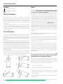
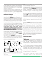
1
Table of contents Oscilloscope datasheet St. 170698/hüb/goRR Operating Instructions Symbols ............................................................ General Information ........................................... Use of tilt handle ............................................... Safety ................................................................ Operating conditions ......................................... Warranty ............................................................ Maintenance ..................................................... Protective Switch-Off ........................................ Power supply .................................................... Type of signal voltage ........................................ Amplitude Measurements ................................. Time Measurements ......................................... Connection of Test Signal ................................. First Time Operation .......................................... Trace Rotation TR .............................................. Probe compensation and use ............................ Operating Modes of the Y Amplifier ................. X-Y Operation .................................................... Phase difference measurement in DUAL mode ............................................ Measurement of an amplitude modulation ....... Triggering and Timebase ................................... Automatic Triggering ......................................... Normal Triggering, Slope ................................... Trigger Coupling ................................................ Triggering of Video Signals ................................ Line Triggering ................................................... Alternate Triggering ........................................... External Triggering ............................................ Trigger Indicator ................................................ Function of variable HOLD OFF control ............. Y Overscanning Operation ................................ Component Tester ............................................ Test Patterns ..................................................... Test Instructions General .............................................................. Cathode-Ray Tube: Brightness, Focus, Linearity, Raster Distortions ......... Astigmatism Check ........................................... Symmetry and Drift of the Vertical Amplifier .... Calibration of the Vertical Amplifier ................... Transmission Performance of the Vertical Amplifier ................................. Subject to change without notice 6 6 6 6 7 7 7 7 7 8 8 9 10 12 12 12 14 15 15 16 16 17 17 17 17 17 17 17 17 17 18 18 22 23 23 23 23 23 24 Oscilloscope GB HM 303-4 Operating Modes:CHI/II-TRIG.I/II, DUAL, ADD, CHOP., INV.I/II and XY-Operation ................. Triggering Checks .............................................. Timebase ........................................................... Component Tester ............................................ Trace Alignment ................................................ 24 25 25 26 26 Service Instructions General .............................................................. Instrument Case Removal ................................. Operating Voltages ............................................ Maximum and Minimum Brightness ................. Astigmatism control .......................................... Trigger Threshold .............................................. Trouble-Shooting the Instrument ....................... Replacement of Components and Parts ........... Adjustments ...................................................... 27 27 27 27 27 28 28 28 28 Short Instruction . ............................................... Front Panel Elements, Front View . .................. 29 30 1 General information regarding the CE marking HAMEG instruments fulfill the regulations of the EMC directive. The conformity test made by HAMEG is based on the actual generic- and product standards. In cases where different limit values are applicable, HAMEG applies the severer standard. For emission the limits for residential, commercial and light industry are applied. Regarding the immunity (susceptibility) the limits for industrial environment have been used. The measuring- and data lines of the instrument have much influence on emmission and immunity and therefore on meeting the acceptance limits. For different applications the lines and/or cables used may be different. For measurement operation the following hints and conditions regarding emission and immunity should be observed: 1. Data cables For the connection between instruments resp. their interfaces and external devices, (computer, printer etc.) sufficiently screened cables must be used. Without a special instruction in the manual for a reduced cable length, the maximum cable length of a dataline must be less than 3 meters long. If an interface has several connectors only one connector must have a connection to a cable. Basically interconnections must have a double screening. For IEEE-bus purposes the double screened cables HZ72S and HZ72L from HAMEG are suitable. 2. Signal cables Basically test leads for signal interconnection between test point and instrument should be as short as possible. Without instruction in the manual for a shorter length, signal lines must be less than 3 meters long. Signal lines must screened (coaxial cable - RG58/U). A proper ground connection is required. In combination with signal generators double screened cables (RG223/U, RG214/U) must be used. 3. Influence on measuring instruments. Under the presence of strong high frequency electric or magnetic fields, even with careful setup of the measuring equipment an influence of such signals is unavoidable. This will not cause damage or put the instrument out of operation. Small deviations of the measuring value (reading) exceeding the instruments specifications may result from such conditions in individual cases. December 1995 HAMEG GmbH KONFORMITÄTSERKLÄRUNG DECLARATION OF CONFORMITY DECLARATION DE CONFORMITE Name und Adresse des Herstellers Manufacturer´s name and address Nom et adresse du fabricant ® Instruments HAMEG GmbH Kelsterbacherstraße 15-19 D - 60528 Frankfurt HAMEG S.a.r.l. 5, av de la République F - 94800 Villejuif Die HAMEG GmbH / HAMEG S.a.r.l bescheinigt die Konformität für das Produkt The HAMEG GmbH / HAMEG S.a.r.l herewith declares conformity of the product HAMEG GmbH / HAMEG S.a.r.l déclare la conformite du produit Bezeichnung / Product name / Designation: Oszilloskop/Oscilloscope/Oscilloscope Typ / Type / Type: HM303-4 mit / with / avec: - Optionen / Options / Options: - mit den folgenden Bestimmungen / with applicable regulations / avec les directives suivantes EMV Richtlinie 89/336/EWG ergänzt durch 91/263/EWG, 92/31/EWG EMC Directive 89/336/EEC amended by 91/263/EWG, 92/31/EEC Directive EMC 89/336/CEE amendée par 91/263/EWG, 92/31/CEE Niederspannungsrichtlinie 73/23/EWG ergänzt durch 93/68/EWG Low-Voltage Equipment Directive 73/23/EEC amended by 93/68/EEC Directive des equipements basse tension 73/23/CEE amendée par 93/68/CEE Angewendete harmonisierte Normen / Harmonized standards applied / Normes harmonisées utilisées Sicherheit / Safety / Sécurité EN 61010-1: 1993 / IEC (CEI) 1010-1: 1990 A 1: 1992 / VDE 0411: 1994 Überspannungskategorie / Overvoltage category / Catégorie de surtension: II Verschmutzungsgrad / Degree of pollution / Degré de pollution: 2 Elektromagnetische Verträglichkeit / Electromagnetic compatibility / Compatibilité électromagnétique EN 50082-2: 1995 / VDE 0839 T82-2 ENV 50140: 1993 / IEC (CEI) 1004-4-3: 1995 / VDE 0847 T3 ENV 50141: 1993 / IEC (CEI) 1000-4-6 / VDE 0843 / 6 EN 61000-4-2: 1995 / IEC (CEI) 1000-4-2: 1995 / VDE 0847 T4-2: Prüfschärfe / Level / Niveau = 2 EN 61000-4-4: 1995 / IEC (CEI) 1000-4-4: 1995 / VDE 0847 T4-4: Prüfschärfe / Level / Niveau = 3 EN 50081-1: 1992 / EN 55011: 1991 / CISPR11: 1991 / VDE0875 T11: 1992 Gruppe / group / groupe = 1, Klasse / Class / Classe = B Datum /Date /Date 14.12.1995 Unterschrift / Signature /Signatur . Dr. J. Herzog Technical Manager Directeur Technique . OSCILLOSCOPES Specifications Vertical Deflection Operating modes: Channel I or II separate, both Channels (alternated or chopped), (Chopper frequency approx. 0.5MHz). Sum or difference with Ch. I and Ch. II (both channels invertable). XY-Mode: via channel I and channel II Frequency range: 2xDC to 30MHz (−3dB) Risetime: <12ns. Overshoot ≤1%. Deflection coefficients: 12 calibrated steps from 5mV/div. to 20V/div. (1-2-5 sequence) with variable 2.5:1 up to 50V/div. Accuracy in calibrated position: ±3% Y-expansion x5 (calibrated) to 1mV/div. (±5%) in the frequency range from DC - 10MHz (–3dB) Input impedance: 1MΩ II 20pF. Input coupling: DC-AC-GD (ground). Input voltage: max. 400V (DC + peak AC). Triggering Automatic: (peak to peak) <20Hz-100MHz (≤ 0.5div.) Normal with level control: DC-100MHz (≤0.5div.) ALT. Triggering; LED indicator for trigger action Slope: positive or negative, Sources: Channel I or II, CH. I alternating CH II, line, external Coupling: AC (10Hz to 100MHz), DC (0 to 100MHz), LF (0 to 1.5kHz) Active TV-Sync-Separator (pos. and neg.) External: ≥0.3Vp-p from 30Hz to 30MHz Horizontal Deflection Time coefficients: 20 calibrated steps from 0.2s/div. - 0.1µs/div. in 1-2-5 sequence Accuracy in calibrated position: ±3%. Min. speed incl. variable 2.5:1: 0.5s/div. with X-Mag. x10: ±5%; 10ns/div.: ±8% Holdoff time: variable to approx. 10:1 Bandwidth X-amplifier: 0-3MHz (−3dB). Input X-Amplifier via Channel II, (sensitivity see Channel II specification) X-Y phase shift: <3° below 220kHz. Component Tester Test voltage: approx. 6Vrms (open circuit). Test current: approx. 5mArms (shorted). Test frequency: approx. 50Hz Test connection: 2 banana jacks 4mm ∅ One test lead is grounded (Safety Earth) General Information CRT: D14-364GY/123 or ER151-GH/-, 6" rectangular screen (8x10cm) internal graticule Acceleration voltage: approx 2000V Trace rotation: adjustable on front panel Calibrator: square-wave generator (tr <4ns) ≈1kHz / 1MHz; Output: 0.2V ±1% and 2V Line voltage: 100-240V AC ±10%, 50/60Hz Power consumption: approx. 36 Watt at 50Hz. Min./Max. ambient temperature: −10°C...+40°C Protective system: Safety class I (IEC 1010-1) Weight: approx. 5.6kg, color: techno-brown Cabinet: W 285, H 125, D 380 mm Lockable tilt handle Subject to change without notice. 3/95 30MHz Standard Oscilloscope HM 303 Dual Channel, DC to 30MHz, 1mV/div.; Overscan Indicator Time Base: 0.5s to 10ns/div.; Variable Holdoff; Alternate Triggering Triggering: DC-100MHz; Auto Peak to Peak; Active TV-Sync-Separator Additional Features: Component Tester, 1kHz/1MHz Calibrator The new HAMEG HM303 oscilloscope succeeds the HM203 (over 170,000 sold worldwide). The bandwidth has been extended from 20 to 30MHz, the sweep rate increased to 10ns/div. and improvements added to the already legendary HAMEG auto triggering system. The HM303 is the ideal instrument for waveform display in the DC to 70MHz frequency range. A key feature of this oscilloscope is the vertical amplifier's pulse fidelity, limiting overshoot to only 1%. The HM303 offers a special fast rise time, 1kHz/1MHz Calibrator permitting high quality probe compensation across the entire frequency range to ensure probe-tip thru to display integrity. An Overscan Indicator assists in vertical display amplitude and position adjustment. The HM303 is capable of triggering on input waveforms over 100MHz and on signal levels as small as 0.5 division. Alternate triggering mode enables the display of two asynchronous signals simultaneously. An active Video SyncSeparator permits detailed examination of complex TV signal inputs. A well proven, built-in component tester is now equipped with a stabilized measuring voltage. The use of a switching type of power supply minimizes both weight and power consumption and universally accepts a wide range of input power line voltages, without the requirement to change jumpers or switch positions. The HM303's CRT is fully mu-metal shielded against outside magnetic fields. HAMEG is setting newprice/performance breakthroughs with the introduction of this fine oscilloscope. This performance packed scope will tempt all users to run it through its paces. Screen photo of 1 MHz square wave signal Screen photo of 50 and 100MHz sine wave with alternate triggering Accessories supplied: Line cord, Operators Manual, 2 Probes 1:1/10:1 OSCILLOSCOPES HZ 56 AC/DC Current Probe Utilising Hall Effect technology to provide a broad frequency response, the probe will accurately measure AC, DC and complex waveforms. The compact clip-on design conforms to the IEC1010 safety standard and allows nonintrusive measurement of current from 5mA to 30A peak to an accuracy of ±1%. The probe gives a voltage output directly proportional to the measured current which is compatible with a wide range of measuring instruments. Specifications: Current range: Accuracy: Dielectric strength: Output sensitivity: 20A DC / 30A AC ± 1% ± 2mA 3.7kV, 50Hz, 1min. 100mV/A Frequency range: Resolution: Load impedance: Divers: DC-100kHz ±1mA >100kΩ BNC-cable, 2m. HZ 72/S/L HZ36 Accessories supplied HZ38 HZ51 HZ 34S HZ52 HZ20 HZ 32 HZ22 HZ 33 HZ53 HZ23 HZ54 HZ 33W HZ24 HZ84-2 HZ20 HZ22 HZ23 HZ24 HZ58 Adaptor BNC to 4mm binding posts 50Ω BNC Feed-through termination 1GHz, 1W Attenuator 2:1, BNC male to BNC female, for oscilloscope service only. Set of 4 BNC 50Ω attenuators; 3/6/10/20dB; 1GHz, 1W, incl. 1x HZ22 HZ39 Spare Cable for HZ36 HZ57 Spare Cable for HZ51, HZ54 Spare-parts for modular probes only Spare-part Kit HZ40 Test Cables HZ32 HZ33 HZ33S HZ33W HZ34 HZ34S HZ72S HZ72L HZ84-2 HZ84-3 Test cable BNC to single stacking banana plugs; 40 inch Coaxial cable BNC/BNC, 50Ω, 20 inch Coaxial cable BNC/BNC, 50Ω, 20 inch, insulated Coaxial cable BNC/BNC, 50Ω, 20 inch, elbow Coaxial cable BNC/BNC, 50Ω, 40 inch Coaxial cable BNC/BNC, 50Ω, 40 inch, insulated IEEE-488-Bus-Cable, 40 inch. double shielded IEEE-488-Bus-Cable, 60 inch, double shielded Spare Printer Cable for HD148 (CE) and HM305 / 1007 (CE) Spare Printer Cable for combination of 25pole D-SUB / 26pole plastic male Wide Band Probes with RF alignment Type HZ36 HZ51 HZ52 HZ53 HZ54 Attenuation Max. Bandwidth Risetime Input Impedance Ratio Input Voltage 1:1/10:1 10/100MHz <35/3.5ns 1/10MΩII57/12pF (10:1) 600V (DC+peak AC) 10:1 150MHz <2.4ns 10MΩII12pF 600V (DC+peak AC) 10:1 250MHz <1.4ns 10MΩII10pF 600V (DC+peak AC) 100:1 100MHz <3.5ns 100MΩII4.5pF 1200V (DC+peak AC) 1:1/10:1 10/150MHz <35/2.4ns 1/10MΩII57/12pF (10:1) 600V (DC+peak AC) Special Probes HZ38 Demodulator Probe 0.1 - 500MHz HZ58 High Voltage Probe, 1000:1; Ri approx. 500MΩ; DC - 1MHz max. 200V (DC) max. 15kV (DC+peak AC) HZ47 Viewing Hood for Oscilloscopes HM205, 408, 604-1+2, 1005 and 1007 HZ48 Viewing Hood for Oscilloscopes 303, 304, 305, 604-3 and 1004 HZ40 HZ39 HZ57 HZ96 Carrying Case for oscilloscopes HM203, 205, 208, 408, 604, 1005 and 1007 HZ97 Carrying Case for HM303, 304, 305, 604-3, 1004 and HM5005 / 6 / 10. The carrying case provides protection during transportation of an oscilloscope. It is made of a durable vinylcoated material that is designed to withstand the stress and wear and tear of field use. Subject to change without notice 05/96 Operating Instructions Symbols Safety See user's manual Danger high voltage Earth General Information This oscilloscope is easy to operate. The logical arrangement of the controls allows anyone to quickly become familiar with the operation of the instrument, however, experienced users are also advised to read through these instructions so that all functions are understood. Immediately after unpacking, the instrument should be checked for mechanical damage and loose parts in the interior. If there is transport damage, the supplier must be informed immediately. The instrument must then not be put into operation. Use of tilt handle To view the screen from the best angle, there are three different positions (C, D, E) for setting up the instrument. If the instrument is set down on the floor after being carried, the handle automatically remains in the upright carrying position (A). In order to place the instrument onto a horizontal surface, the handle should be turned to the upper side of the oscilloscope (C). For the D position (10° inclination), the handle should be turned to the opposite direction of the carrying position until it locks in place automaticallyunderneath the instrument. For the E position (20° inclination),the handle should be pulled to release it from the D position and swing backwards until it locks once more. The handle may also be set to a position for horizontal carrying by turning it to the upper side to lock in the B position. At the same time, the instrument must be lifted, because otherwise the handle will jump back. This instrument has been designed and tested in accordance with IEC Publication 348, Safety Requirements for Electronic Measuring Apparatus. The CENELEC HD401 regulations correspond to this standard. It has left the factory in a safe condition. This instruction manual contains important information and warnings which have to be followed by the user to ensure safe operation and to retain the oscilloscope in a safe condition. The case, chassis and all measuring terminals are connected to the protective earth contact of the appliance inlet. The instrument operates according to Safety Class I (threeconductor power cord with protective earthing conductor and a plug with earthing contact). The mains/line plug shall only be inserted in a socket outlet provided with a protective earth contact. The protective action must not be negated by the use of an extension cord without a protective conductor. The mains/line plug should be inserted before connections are made to measuring circuits. The grounded accessible metal parts (case, sockets, jacks) and the mains/line supply contacts (line/live, neutral) of the instrument have been tested against insulation breakdown with 2200V DC. Under certain conditions, 50Hz or 60Hz hum voltages can occur in the measuring circuit due to the interconnection with other mains/line powered equipment or instruments. This can be avoided by using an isolation transformer (Safety Class II) between the mains/line outlet and the power plug of the device being investigated. Most cathode-ray tubes develop X-rays. However, the dose equivalent rate falls far below the maximum permissible value of 36pA/kg (0.5mR/h). Whenever it is likely that protection has been impaired, the instrument shall be made inoperative and be secured against any unintended operation. The protection is likely to be impaired if, for example, the instrument − shows visible damage, − fails to perform the intended measurements, − has been subjected to prolonged storage under unfavourable conditions (e.g. in the open or in moist environments), − has been subject to severe transport stress (e.g. in poor packaging). 6 Subject to change without notice Operating conditions The instrument has been designed for indoor use. The permissible ambient temperature range during operation is +10°C (+50°F) ... +40°C (+104°F). It may occasionally be subjected to temperatures between +10°C (+50°F) and 10°C (+14°F) without degrading its safety. The permissible ambient temperature range for storage or transportation is -40°C (-40°F) ... +70°C (+158°F). The maximum operating altitude is up to 2200m (non-operating 15000m). The maximum relative humidity is up to 80%. If condensed water exists in the instrument it should be acclimatized before switching on. In some cases (e.g. extremely cold oscilloscope) two hours should be allowed before the instrument is put into operation. The instrument should be kept in a clean and dry room and must not be operated in explosive, corrosive, dusty, or moist environments. The oscilloscope can be operated in any position, but the convection cooling must not be impaired. The ventilation holes may not be covered. For continuous operation the instrument should be used in the horizontal position, preferably tilted upwards, resting on the tilt handle. The specifications stating tolerances are only valid if the instrument has warmed up for 30 minutes at an ambient temperature between +15°C (+59°F) and +30°C (+86°F). Values without tolerances are typical for an average instrument. Warranty HAMEG warrants to its Customers that the products it manufactures and sells will be free from defects in materials and workmaship for a period of 2 years. This warranty shall not apply to any defect, failure or damage caused by improper use or inadequate maintenance and care. HAMEG shall not obliged to provide service under this warranty to repair damage resulting from attempts by personnel other than HAMEG represantatives to install, repair, service or modify these products. In order to obtain service under this warranty, Customers must contact and notify the distributor who has sold the product. Each instrument is subjected to a quality test with 10 hour burn-in before leaving the production. Practically all early failures are detected by this method. In the case of shipments by post, rail or carrier it is recommended that the original packing is carefully preserved. Transport damages and damage due to gross negligence are not covered by the guarantee. In the case of a complaint, a label should be attached to the housing of the instrument which describes briefly the faults observed. If at the same time the name and telephone number (dialing code and telephone or direct number or department designation) is stated for possible queries, this helps towards speeding up the processing of guarantee claims. Maintenance Various important properties of the oscilloscope should be carefully checked at certain intervals. Only in this way is it largely certain that all signals are displayed with the accuracy on which the technical data are based. The test methods described in the test plan of this manual can be Subject to change without notice performed without great expenditure on measuring instruments. However, purchase of the new HAMEG scope tester HZ 60, which despite its low price is highly suitable for tasks of this type, is very much recommended. The exterior of the oscilloscope should be cleaned regularly with a dusting brush. Dirt which is difficult to remove on the casing and handle, the plastic and aluminium parts, can be removed with a moistened cloth (99% water +1% mild detergent). Spirit or washing benzine (petroleum ether) can be used to remove greasy dirt. The screen may be cleaned with water or washing benzine (but not with spirit (alcohol) or solvents), it must then be wiped with a dry clean lint-free cloth. Under no circumstances may the cleaning fluid get into the instrument. The use of other cleaning agents can attack the plastic and paint surfaces. Protective Switch-Off This instrument is equipped with a switch mode power supply. It has both overvoltage and overload protection, which will cause the switch mode supply to limit power consumption to a minimum. In this case a ticking noise may be heard. Power supply The oscilloscope operates on mains/line voltages between 100VAC and 240VAC. No means of switching to different input voltages has therefore been provided. The power input fuses are externally accessible. The fuseholder is located above the 3-pole power connector. The power input fuses are externally accessible, if the rubber conector is removed. The fuseholder can be released by pressing its plastic retainers with the aid of a small screwdriver. The retainers are located on the right and left side of the holder and must be pressed towards the center. The fuse(s) can then be replaced and pressed in until locked on both sides. Use of patched fuses or short-circuiting of the fuseholder is not permissible; HAMEG assumes no liability whatsoever for any damage caused as a result, and all warranty claims become null and void. Fuse type: Size 5x20mm; 0.8A, 250V AC fuse; must meet IEC specification 127, Sheet III (or DIN 41 662 or DIN 41 571, sheet 3). Time characteristic: time-lag. Attention! There is a fuse located inside the instrument within the switch mode power supply: Size 5x20mm; 0.5A, 250V AC fuse; must meet IEC specification 127, Sheet III (or DIN 41 662 or DIN 41 571, sheet 3). Time characteristic: fast (F). This fuse must not be replaced by the operator! 7 Type of signal voltage With the HM 303, most repetitive signals in the frequency range up to at least 30MHz (−3dB) can be examined. Sinewave signals of 50MHz are displayed with a height of approx. 50% (−6dB). However when examining square or pulse type waveforms, attention must be paid to the harmonic content of such signals. The repetition frequency (fundamental frequency) of the signal must therefore be significantly smaller than the upper limit frequency of the vertical amplifier. Displaying composite signals can be difficult, especially if they contain no repetive higher amplitude content which can be used for triggering. This is the case with bursts, for instance. To obtain a well-triggered display in this case, the assistance of the variable holdoff and/or variable time control may be required. Television video signals are relatively easy to trigger using the built-in TV-SyncSeparator (TV). For optional operation as a DC or AC voltage amplifier, the vertical amplifier input is provided with a DC/AC switch. The DC position should only be used with a seriesconnected attenuator probe or at very low frequencies or if the measurement of the DC voltage content of the signal is absolutely necessary. When displaying very low frequency pulses, the flat tops may be sloping with AC coupling of the vertical amplifier (AC limit frequency approx. 1.6 Hz for 3dB). In this case, DC operation is preferred, provided the signal voltage is not superimposed on a too high DC level. Otherwise a capacitor of adequate capacitance must be connected to the input of the vertical amplifier with DC coupling. This capacitor must have a sufficiently high breakdown voltage rating. DC coupling is also recommended for the display of logic and pulse signals, especially if the pulse duty factor changes constantly. Otherwise the display will move upwards or downwards at each change. Pure direct voltages can only be measured with DC-coupling. difference in Vpp. The relationship between the different voltage magnitudes can be seen from the following figure. Vp Vrms Vmom Vpp Voltage values of a sine curve Vrms = effective value; Vp = simple peak or crest value; Vpp = peak-to-peak value; Vmom = momentary value. The minimum signal voltage which must be applied to the Y input for a trace of 1div. height is 1mVpp when the YMAG. x5 pushbutton is depressed, the VOLTS/DIV. switch is set to 5mV/div., and the vernier is set to CAL by turning the fine adjustment knob of the VOLTS/DIV. switch fully clockwise. However, smaller signals than this may also be displayed. The deflection coefficients on the input attenuators are indicated in mV/div. or V/div. (peak-to-peak value). The magnitude of the applied voltage is ascertained by multiplying the selected deflection coefficient by the vertical display height in div. If an attenuator probe x10 is used, a further multiplication by a factor of 10 is required to ascertain the correct voltage value. For exact amplitude measurements, the variable control on the attenuator switch must be set to its calibrated detent CAL. When turning the variable control ccw, the sensitivity will be reduced by a factor of 2.5. Therefore every intermediate value is possible within the 1-2-5 sequence. With direct connection to the vertical input, signals up to 400Vpp may be displayed (attenuator set to 20V/div., variable control to left stop). Amplitude Measurements With the designations In general electrical engineering, alternating voltage data normally refers to effective values (rms = root-meansquare value). However, for signal magnitudes and voltage designations in oscilloscope measurements, the peak-topeak voltage (Vpp) value is applied. The latter corresponds to the real potential difference between the most positive and most negative points of a signal waveform. If a sinusoidal waveform, displayed on the oscilloscope screen, is to be converted into an effective (rms) value, the resulting peak-to-peak value must be divided by 2x√2 = 2.83. Conversely, it should be observed that sinusoidal voltages indicated in Vrms (Veff) have 2.83 times the potential 8 H = display height in div., U = signal voltage in Vpp at the vertical input, D = deflection coefficient in V/div. at attenuator switch, the required value can be calculated from the two given quantities: U=D·H H= U D D= U H However, these three values are not freely selectable. They have to be within the following limits (trigger threshold, accuracy of reading): Subject to change without notice Voltage DC + ACpeak = 400Vmax. H between 0.5 and 8div., if possible 3.2 to 8div., U between 1mVpp and 160Vpp, D between 1mV/div. and 20V/div. in 1-2-5 sequence. Examples: Set deflection coefficient D = 50mV/div. 0.05V/div., observed display height H = 4.6div., required voltage U = 0.05·4.6 = 0.23Vpp. Input voltage U = 5Vpp, set deflection coefficient D = 1V/div., required display height H = 5:1 = 5div. Signal voltage U = 230Vrms·2√2 = 651Vpp (voltage > 160Vpp, with probe 10:1: U = 65.1Vpp), desired display height H = min. 3.2div., max. 8div., max. deflection coefficient D = 65.1:3.2 = 20.3V/div., min. deflection coefficient D = 65.1:8 = 8.1V/div., adjusted deflection coefficient D = 10V/div. The input voltage must not exceed 400V, independent from the polarity. If an AC voltage which is superimposed on a DC voltage is applied, the maximum peak value of both voltages must not exceed + or –400V. So for AC voltages with a mean value of zero volt the maximum peak to peak value is 800Vpp. If attenuator probes with higher limits are used, the probes limits are valid only if the oscilloscope is set to DC input coupling. If DC voltages are applied under AC input coupling conditions the oscilloscope maximum input voltage value remains 400V. The attenuator consists of a resistor in the probe and the 1MΩ input resistor of the oscilloscope, which are disabled by the AC input coupling capacity when AC coupling is selected. This also applies to DC voltages with superimposed AC voltages. It also must be noted that due to the capacitive resistance of the AC input coupling capacitor, the attenuation ratio depends on the signal frequency. For sinewave signals with frequencies higher than 40Hz this influence is negligible. In the GD (ground coupling) setting, the signal path is interrupted directly beyond the input. This causes the attenuator to be disabled again, but now for both DC and AC voltages. With the above listed exceptions HAMEG 10:1 probes can be used for DC measurements up to 600V or AC voltages (with a mean value of zero volt) of 1200Vpp. The 100:1 probe HZ53 allows for 1200V DC or 2400Vpp for AC. It should be noted that its ACpeak value is derated at higher frequencies. If a normal x10 probe is used to measure high voltages there is the risk that the compensation trimmer bridging the attenuator series resistor will break down causing damage to the input of the oscilloscope. However, if for example only the residual ripple of a high voltage is to be displayed on the oscilloscope, a normal x10 probe is sufficient. In this case, an appropriate high voltage capacitor (approx. 22-68nF) must be connected in series with the input tip of the probe. Subject to change without notice peak AC DC DC AC time Total value of input voltage The dotted line shows a voltage alternating at zero volt level. If superimposed on a DC voltage, the addition of the positive peak and the DC voltage results in the max. voltage (DC + ACpeak). With Y-POS. control (input coupling to GD) it is possible to use a horizontal graticule line as reference line for ground potential before the measurement. It can lie below or above the horizontal central line according to whether positive and/or negative deviations from the ground potential are to be measured. Time Measurements As a rule, most signals to be displayed are periodically repeating processes, also called periods. The number of periods per second is the repetition frequency. Depending on the time base setting of the TIME/DIV. switch, one or several signal periods or only a part of a period can be displayed. The time coefficients are stated in s/div., ms/ div. and µs/div. on the TIME/DIV.-switch. The scale is accordingly divided into three fields. The duration of a signal period or a part of it is determined by multiplying the relevant time (horizontal distance in div.) by the time coefficient set on the TIME/DIV.-switch. The variable time control (identified with an arrow knob cap) must be in its calibrated position CAL. (arrow pointing horizontally to the right). With the designations L = displayed wave length in div. of one period, T = time in seconds for one period, F = recurrence frequency in Hz of the signal, Tc = time coefficient in s/div. on timebase switch and the relation F = 1/T, the following equations can be stated: T = L · Tc F= 1 L · Tc T Tc 1 L= F · Tc L= T L 1 Tc = L · F Tc = With depressed X-MAG. (x10) pushbutton the Tc value must be divided by 10. However, these four values are not freely selectable. They have to be within the following limits: L between 0.2 and 10div., if possible 4 to 10div., T between 0.01µs and 2s, F between 0.5Hz and 30MHz, Tc between 0.1µs/div. and 0.2s/div. in 1-2-5 sequence (with X-MAG. (x10) in out position), and Tc between 10ns/div. and 20ms/div. in 1-2-5 sequence (with pushed X-MAG. (x10) pushbutton). 9 Examples: Displayed wavelength L = 7div., set time coefficient Tc = 0.1µs/div., required period T = 7x0.1x10−6 = 0.7µs required rec. freq. F = 1:(0.7x10⁻⁶) = 1.428MHz. Signal period T = 1s, set time coefficient Tc = 0.2s/div., required wavelength L = 1:0.2 = 5div.. Displayed ripple wavelength L = 1div., set time coefficient Tc = 10ms/div., required ripple freq. F = 1:(1x10x10−3) = 100Hz. TV-line frequency F = 15625Hz, set time coefficient Tc = 10µs/div., required wavelength L = 1:(15 625x10−5) = 6.4div.. Sine wavelength L = min. 4div., max. 10div., Frequency F = 1kHz, max. time coefficient Tc = 1:(4x10³) = 0.25ms/div., min. time coefficient Tc = 1:(10x103) = 0.1ms/div., set time coefficient Tc = 0.2ms/div., required wavelength L = 1:(103x0.2x10−3) = 5div. Displayed wavelength L = 0.8div., set time coefficient Tc = 0.5µs/div., pressed X-MAG. (x10) button: Tc = 0.05µs/div., required rec. freq. F = 1:(0.8x0.05x10−6) = 25MHz, required period T = 1:(25x10−6) = 40ns. If the time is relatively short as compared with the complete signal period, an expanded time scale should always be applied (X-MAG. (x10) button pressed). In this case, the ascertained time values have to be divided by 10. The time interval of interest can be shifted to the screen center using the X-POS. control. When investigating pulse or square waveforms, the critical feature is the risetime of the voltage step. To ensure that transients, ramp-offs, and bandwidth limits do not unduly influence the measuring accuracy, the risetime is generally measured between 10% and 90% of the vertical pulse height. For measurement adjust the Y attenuator switch with its variable control together with the Y-POS. control so that the pulse height is precisely aligned with the 0 and 100% lines of the internal graticule. The 10% and 90% points of the signal will now coincide with the 10% and 90% graticule lines. The risetime is given by the product of the horizontal distance in div. between these two coincidence points and the time coefficient setting. If X x10 magnification is used, this product must be divided by 10. The fall time of a pulse can also be measured by using this method. The following figure shows correct positioning of the oscilloscope trace for accurate risetime measurement. 10 With a time coefficient of 0.2µs/div. and pushed X-MAG x10 button the example shown in the above figure results in a measured total risetime of ttot = 1.6div·0.2µs/div.:10 = 32ns When very fast risetimes are being measured, the risetimes of the oscilloscope amplifier and of the attenuator probe has to be deducted from the measured time value. The risetime of the signal can be calculated using the following formula. tr = √ttot2 - tosc2 - tp2 In this ttot is the total measured risetime, tosc is the risetime of the oscilloscope amplifier (approx. 12ns), and tp the risetime of the probe (e.g. = 2ns). If ttot is greater than 100ns, then ttot can be taken as the risetime of the pulse, and calculation is unnecessary. Calculation of the example in the figure above results in a signal risetime tr = √ 322 - 122 - 22 = 29.6ns The measurement of the rise or fall time is not limited to the trace dimensions shown in the above diagram. It is only particularly simple in this way. In principle it is possible to measure in any display position and at any signal amplitude. It is only important that the full height of the signal edge of interest is visible in its full length at not too great steepness and that the horizontal distance at 10% and 90% of the amplitude is measured. If the edge shows rounding or overshooting, the 100% should not be related to the peak values but to the mean pulse heights. Breaks or peaks (glitches) next to the edge are also not taken into account. With very severe transient distortions, the rise and fall time measurement has little meaning. For amplifiers with approximately constant group delay (therefore good pulse transmission performance) the following numerical relationship between rise time tr (in ns) and bandwidth B (in MHz) applies: tr = 350 B B= 350 tr Connection of Test Signal Caution: When connecting unknown signals to the oscilloscope input, always use automatic triggering and set the DC-AC input coupling switch toAC. The attenuator switch should initially be set to 20V/div. Subject to change without notice Sometimes the trace will disappear after an input signal has been applied. The attenuator switch must then be turned back to the left, until the vertical signal height is only 3-8div. With a signal amplitude greater than 160Vpp, an attenuator probe must be inserted before the vertical input. If, after applying the signal, the trace is nearly blanked, the period of the signal is probably substantially longer than the set value on the TIME/DIV. switch. It should be turned to the left to an adequately larger time coefficient. utilized (e.g. for pulses with steep edges) we strongly advise using the modular probes HZ 51 (x10) HZ 52 (x10 HF) and HZ 54 (x1 and x10. This can save the purchase of an oscilloscope with larger bandwidth and has the advantage that defective components can be ordered from HAMEG and replaced by oneself. The probes mentioned have a HF-calibration in addition to low frequency calibration adjustment. Thus a group delay correction to the upper limit frequency of the oscilloscope is possible with the aid of an 1MHz calibrator, e.g. HZ60. The signal to be displayed can be connected directly to the Y-input of the oscilloscope with a shielded test cable such as HZ 32 or HZ 34, or reduced through a x10 or x100 attenuator probe. The use of test cables with high impedance circuits is only recommended for relatively low frequencies (up to approx. 50 kHz). For higher frequencies, the signal source must be of low impedance, i.e. matched to the characteristic resistance of the cable (as a rule 50 Ohm). Especially when transmitting square and pulse signals, a resistor equal to the characteristic impedance of the cable must also be connected across the cable directly at the Y-input of the oscilloscope. When using a 50Ω cable such as the HZ 34, a 50Ω through termination type HZ22 is available from HAMEG. When transmitting square signals with short rise times, transient phenomena on the edges and top of the signal may become visible if the correct termination is not used. A terminating resistance is sometimes recommended with sine signals as well. Certain amplifiers, generators or their attenuators maintain the nominal output voltage independent of frequency only if their connection cable is terminated with the prescribed resistance. Here it must be noted that the terminating resistor HZ22 will only dissipate a maximum of 2 Watts. This power is reached with 10 Vrms or at 28.3 Vpp with sine signal. In fact the bandwidth and rise time of the oscilloscope are not noticably changed with these probe types and the waveform reproduction fidelity can even be improved because the probe can be matched to the oscilloscopes individual pulse response. If a x10 or x100 attenuator probe is used, no termination is necessary. In this case, the connecting cable is matched directly to the high impedance input of the oscilloscope. When using attenuators probes, even high internal impedance sources are only slightly loaded (approx. 10 MΩ II 16 pF or 100 MΩ II 9 pF with HZ 53). Therefore, if the voltage loss due to the attenuation of the probe can be compensated by a higher amplitude setting, the probe should always be used. The series impedance of the probe provides a certain amount of protection for the input of the vertical amplifier. Because of their separate manufacture, all attenuator probes are only partially compensated, therefore accurate compensation must be performed on the oscilloscope (see “Probe compensation page M7). Standard attenuator probes on the oscilloscope normally reduce its bandwidth and increase the rise time. In all cases where the oscilloscope bandwidth must be fully Subject to change without notice If a x10 or x100 attenuator probe is used, DC input coupling must always be used at voltages above 400V. With AC coupling of low frequency signals, the attenuation is no longer independent of frequency, pulses can show pulse tilts. Direct voltages are suppressed but load the oscilloscope input coupling capacitor concerned. Its voltage rating is max. 400 V (DC + peak AC). DC input coupling is therefore of quite special importance with a x100 attenuation probe which usually has a voltage rating of max. 1200 V (DC + peak AC). A capacitor of corresponding capacitance and voltage rating may be connected in series with the attenuator probe input for blocking DC voltage (e.g. for hum voltage measurement). With all attenuator probes, themaximum AC input voltage must be derated with frequency usually above 20kHz. Therefore the derating curve of the attenuator probe type concerned must be taken into account. The selection of the ground point on the test object is important when displaying small signal voltages. It should always be as close as possible to the measuring point. If this is not done, serious signal distortion may result from spurious currents through the ground leads or chassis parts. The ground leads on attenuator probes are also particularly critical. They should be as short and thick as possible. When the attenuator probe is connected to a BNC-socket, a BNC-adapter, which is often supplied as probe accessory, should be used. In this way ground and matching problems are eliminated. Hum or interference appearing in the measuring circuit (especially when a small deflection coefficient is used) is possibly caused by multiple grounding because equalizing currents can flow in the shielding of the test cables (voltage drop between the protective conductor connections, caused by external equipment connected to the mains/line, e.g. signal generators with interference protection capacitors). 11 First Time Operation Before applying power to the oscilloscope it is recommended that the following simple procedures are performed: • Check that all pushbuttons are in the out position, i.e. released. • Rotate the variable controls with arrows, i.e. TIME/DIV. variable control, CH.I and CH.II attenuator variable controls, and HOLD OFF control to their calibrated detent. • Set all controls with marker lines to their midrange position (marker lines pointing vertically). • The TRIG. selector lever switch in the X-field should be set to the position uppermost. • Both GD input coupling pushbutton switches for CH.I and CH.II in the Y-field should be set to theGD position. Switch on the oscilloscope by depressing the red POWER pushbutton. An LED will illuminate to indicate working order. The trace, displaying one baseline, should be visible after a short warm-up period of approx. 10 seconds. AdjustY-POS.I andX-POS. controls to center the baseline. Adjust INTENS. (intensity) and FOCUS controls for medium brightness and optimum sharpness of the trace. The oscilloscope is now ready for use. If only a spot appears (CAUTION! CRT phosphor can be damaged), reduce the intensity immediately and check that the XY pushbutton is in the released (out) position. If the trace is not visible, check the correct positions of all knobs and switches (particularly AT/NORM. button in out position). To obtain the maximum life from the cathode-ray tube, the minimum intensity setting necessary for the measurement in hand and the ambient light conditions should be used. Particular care is required when a single spot is displayed, as a very high intensity setting may cause damage to the fluorescent screen of the CRT. Switching the oscilloscope off and on at short intervals stresses the cathode of the CRT and should therefore be avoided. The instrument is so designed that even incorrect operation will not cause serious damage. The pushbuttons control only minor functions, and it is recommended that before commencement of operation all pushbuttons are in the “out” position. After this the pushbuttons can be operated depending upon the mode of operation required. The HM303 accepts all signals from DC (direct voltage) up to a frequency of at least 30MHz (−3dB). For sinewave voltages the upper frequency limit will be 50MHz (−6dB). 12 However, in this higher frequency range the vertical display height on the screen is limited to approx. 4-5div. The time resolution poses no problem. For example, with 50MHz and the fastest adjustable sweep rate (10ns/div.), one cycle will be displayed every 2div. The tolerance on indicated values amounts to ±3% in both deflection directions. All values to be measured can therefore be determined relatively accurately. However, from approximately 10MHz upwards the measuring error will increase as a result of loss of gain. At 18MHz this reduction is about 10%. Thus, approximately 11% should be added to the measured voltage at this frequency. As the bandwidth of the amplifiers may differ slightly (normally between 30 and 35MHz), the measured values in the upper frequency range cannot be defined exactly. Additionally, as already mentioned, for frequencies above 30MHz the dynamic range of the display height steadily decreases. The vertical amplifier is designed so that the transmission performance is not affected by its own overshoot. Trace Rotation TR In spite of Mumetal-shielding of the CRT, effects of the earths magnetic field on the horizontal trace position cannot be completely avoided. This is dependent upon the orientation of the oscilloscope on the place of work. A centred trace may not align exactly with the horizontal center line of the graticule. A few degrees of misalignment can be corrected by a potentiometer accessible through an opening on the front panel marked TR. Probe compensation and use To display an undistorted waveform on an oscilloscope, the probe must be matched to the individual input impedance of the vertical amplifier. For this purpose a square wave signal with a very fast rise time and minimum overshoot should be used, as the sinusoidal contents cover a wide frequency range. The frequency accuracy and the pulse duty factor are not of such importance. The built-in calibration generator provides a square wave signal with a very fast risetime (<4ns), and switchselectable frequencies of approx. 1kHz and 1MHz from two output sockets below the CRT screen. This signal should not be used for frequency calibration! Subject to change without notice One output provides 0.2Vpp ±1% (tr <4ns) for 10:1 probes, and the other 2Vpp ±1% for 100:1 probes. When the attenuator switches are set to5mV/div vertical deflection coefficient, these calibration voltages correspond to a screen amplitude of 4div. The output sockets have an internal diameter of 4.9mm to accommodate the internationally accepted shielding tube diameter of modern Modular Probes and F-series slimline probes. Only this type of construction ensures the extremly short ground connections which are essential for an undistorted waveform reproduction of non-sinusoidal high frequency signals. Adjustment at 1kHz The C-trimmer adjustment compensates the capacitive loading on the oscilloscope input (approx. 20 pF for the HM 303). By this adjustment, the capacitive division assumes the same ratio as the ohmic voltage divider to ensure the same division ratio for high and low frequencies, as for DC. (For 1:1 probes or switchable probes set to 1:1, this adjustment is neither required nor possible). A baseline exactly parallel to the horizontal graticule lines is a major condition for accurate probe adjustments. (See also “Trace rotation TR”). Connect the probes (Types HZ51, 52, 53, 54, or HZ36) to the CH.I input. All pushbuttons should be released (in the out position). Set input coupling to DC, the attenuator to 5 mV/div., and TIME/DIV. switch to 0.2 ms/div., and all variable controls to CAL. position. Plug the the probe tip into the appropriate calibrator output socket, i.e. 10:1 probes into the 0.2V socket, 100:1 probes into the 2V socket. 1 kHz incorrect correct incorrect Only this compensative adjustment ensures optimum utilisation of the full bandwidth, together with constant group delay at the high frequency end, thereby reducing characteristic transient distortion near the leading edge (e.g. overshoot, rounding, ringing, holes or bumps) to an absolute minimum. Using the probes HZ51, 52 and 54, the full bandwidth of the HM303 can be utilized without risk of unwanted waveform distortion. Prerequisite for this HF compensation is a square wave generator with fast risetime (typically 4 ns), and low output impedance (approx. 50Ω), providing 0.2V and 2V at a frequency of approx. 1MHz. The calibrator output of the HM303 meets these requirements when the CAL. pushbutton is depressed. Connect the probe to CH.I input. Depress the CAL. pushbutton for 1MHz. All other pushbuttons should be released (out position). Set the CH.I input coupling to DC, attenuator switch to 5mV/div, and TIME/DIV. switch to 0.2µs/div. Set all variable controls to CAL. position. Insert the probe tip into the output socket marked 0.2V. A waveform will be displayed on the CRT screen, with leading and trailing edges clearly visible. For the HFadjustment now to be performed, it will be necessary to observe the rising edge as well as the upper left corner of the pulse top. The connecting boxes of the HZ51 and HZ54 contain one R-trimmer screw each, while that of the HZ52 provides three. These R-trimmers have to be adjusted such that the beginning of the pulse is as straight as possible. Overshoot or excessive rounding are unacceptable. This is relatively easy on the HZ51 and HZ54, but slightly more difficult on the HZ52. The rising edge should be as steep as possible, with a pulse top remaining as straight and horizontal as possible. On the HZ52, each of the three trimmers has a clearly defined area of influence on the waveform shape (see Fig.), offering the added advantage of being able to straighten out waveform abberations near the leading edge. HZ51, HZ54 Approximately 2 complete waveform periods are displayed on the CRT screen. Now the compensation trimmer has to be adjusted. Normally, this trimmer is located in the probe head. On the 100:1 probe HZ53, however, it is located in the connecting box at the other end of the cable. Adjust the trimmer with the insulating screw driver provided until the tops of the square wave signal are exactly parallel to the horizontal graticule lines (see 1 kHz diagram). The signal height should then be 4 div. ± 0.12div. (= 3 %). During this adjustment, the signal edges will remain invisible. Adjustment at 1MHz Probes HZ51, 52 and 54 can also be HF-compensated. They incorporate resonance de-emphasing networks (Rtrimmer in conjunction with inductances and capacitors) which permit probe compensation in the range of the upper frequency limit of the vertical oscilloscope amplifier. Subject to change without notice (LF) (LF) T3: alters the middle frequencies T4: alters the leading edge T5: alters the lower frequencies 13 After completion of the HF-adjustment, the signal amplitude displayed on the CRT screen should have the same value as during the 1kHz adjustment. incorrect incorrect correct Adjustment 1MHz Probes other than those mentioned above, normally have a larger tip diameter and may not fit into the calibrator outputs. Whilst it is not difficult for an experienced operator to build a suitable adapter, it should be pointed out that most of these probes have a slower risetime with the effect that the total bandwidth of scope together with probe may fall far below that of the HM303. Furthermore, the HF-adjustment feature is nearly always missing so that waveform distortion can not be entirely excluded. Operating modes of the vertical amplifiers The vertical amplifier is set to the desired operating mode by using the 3 pushbuttons (CH I/II, DUAL and ADD) in the Y field of the front panel. For Mono mode all 3 buttons must be in their released positions; only channel I can then be operated. The button CH I/II-TRIG.I/II must be depressed in mono mode for Channel II. The internal triggering is simultaneously switched over to Channel II with this button. If the DUAL button is depressed, both channels are working. Two signals can be displayed together in this button position (alternate mode) if the time-base setting and the repetition frequency of the signal are suited. This mode is not suitable for displaying very slow-running processes. The display then flickers too much or it appears to jump. If the ADD button is depressed in addition to DUAL, both channels are switched over constantly at a high frequency within a sweep period (CHOP mode). Low frequency signals below 1kHz, or with periods longer than 1ms are then also displayed without flicker. CHOP mode is not recommended for signals with higher repetition frequencies. If only the ADD button is depressed, the signals of both channels are algebraically added (±I ±II). Whether the resulting display shows thesum ordifference is dependent on the phase relationship or the polarity of the signals and on the positions of the INVERT buttons. In-phase input voltages: The adjustment sequence must be followed in the order described, i.e. first at 1kHz, then at 1MHz. The calibrator frequencies should not be used for timebase calibration. The pulse duty cycle deviates from 1:1 ratio. Prerequisites for precise and easy probe adjustments, as well as checks of deflection coefficients, are straight horizontal pulse tops, calibrated pulse amplitude, and zero-potential at the pulse base. Frequency and duty cycle are relatively uncritical. For interpretation of transient response, fast pulse risetimes and low-impedance generator outputs are of particular importance. Providing these essential features, as well as switchselectable output-frequencies, the calibrator of the HM303 can, under certain conditions, replace expensive squarewave generators when testing or compensating wideband-attenuators or -amplifiers. In such a case, the input of an appropriate circuit will be connected to one of the CAL.-outputs via a suitable probe. The voltage provided at a high-impedance input (1MΩII1550pF) will correspond to the division ratio of the probe used (10:1 = 20mVpp, 100:1 = also 20mVpp from 2V output). Suitable probes are HZ51, 52, 53, and 54. 14 Both INVERT CH.I and INVERT CH.II buttons released or depressed = sum. Only one INVERT button depressed = difference. Antiphase input voltages: Both INVERT buttons released or depressed = difference. INVERT CH.Ior INVERT CH.II button depressed = sum. In theADD mode the vertical display position is dependent upon the Y-POS. setting of both channels. The same attenuator switch position is normally used for both channels with algebraic addition. Please note that the Y-POS. settings are added too but are not affected by the INVERT pushbuttons. Differential measurement techniques allow direct measurement of the voltage drop across floating components (both ends above ground). Two identical probes should be used for both vertical inputs. In order to avoid ground loops, use a separate ground connection and do not use the probe ground leads or cable shields. Subject to change without notice X-Y Operation The following must be noted here: For X-Y operation, the pushbutton in the X field marked XY must be depressed. The X signal is then derived from the INPUT CH II (X). The calibration of the X signal during X-Y operation is determined by the setting of the Channel II input attenuator and variable control. − Because of the periodic nature of the trigonometric functions, the calculation should be limited to angles ≤90°. However here is the advantage of the method. This means that the sensitivity ranges and input impedances are identical for both the X and Y axes. However, the Y-POS.II control is disconnected in this mode. Its function is taken over by the X-POS. control. It is important to note that the X-MAG. (x10) facility, normally used for expanding the sweep, should not be operated in the X-Y mode. It should also be noted that the bandwidth of the X amplifier is≥3MHz (−3dB), and therefore an increase in phase difference between both axes is noticeable from 50kHz upwards. The inversion of the X-input signal using theINVERT CH.II button is not possible. Lissajous figures can be displayed in the X-Y mode for certain measuring tasks: − Comparing two signals of different frequency or bringing one frequency up to the frequency of the other signal. This also applies for whole number multiples or fractions of the one signal frequency. − Do not use a too high test frequency. The phase shift of the two oscilloscope amplifiers of the HM 303 in the X-Y mode can exceed an angle of 3° above 120 kHz. − It cannot be seen as a matter of course from the screen display if the test voltage leads or lags the reference voltage. A CR network before the test voltage input of the oscilloscope can help here. The 1 MΩ input resistance can equally serve as R here, so that only a suitable capacitor C needs to be connected in series. If the aperture width of the ellipse is increased (compared with C short-circuited), then the test voltage leads the reference voltage and vice versa. This applies only in the region up to 90° phase shift. Therefore C should be sufficiently large and produce only a relatively small just observable phase shift. Should both input voltages be missing or fail in the X-Y mode, a very bright light dot is displayed on the screen. This dot can burn into the phosphor at a too high brightness setting (INTENS. knob) which causes either a lasting loss of brightness, or in the extreme case, complete destruction of the phosphor at this point. − Phase comparison between two signals of the same frequency. Phase comparison with Lissajous figures The following diagrams show two sine signals of the same frequency and amplitude with different phase angles. Calculation of the phase angle or the phase shift between the X and Y input voltages (after measuring the distances a and b on the screen) is quite simple with the following formula, and a pocket calculator with trigonometric functions. Apart from the reading accuracy, the signal height has no influence on the result. sin ϕ = a b cos ϕ = √ 1− − ( ba ) 2 ϕ = arc sin a b Subject to change without notice Phase difference measurement in DUAL mode A larger phase difference between two input signals of the same frequency and shape can be measured very simply on the screen in Dual mode (DUAL button depressed). The time base should be triggered by the reference signal (phase position 0). The other signal can then have a leading or lagging phase angle. Alternate mode should be selected for frequencies ≥1 kHz; the Chop mode is more suitable for frequencies <1 kHz (less flickering). For greatest accuracy adjust not much more than one period and approximately the same height of both signals on the screen. The variable controls for amplitude and time base and the LEVEL knob can also be used for this adjustment without influence on the result. Both base lines are set onto the horizontal graticule center line with the Y-POS. knobs before the measurement. With sinusoidal signals, observe the zero (crossover point) transitions; the sine peaks are less accurate. If a sine signal is noticeably distorted by even harmonics, or if a d.c. voltage is present, AC coupling is recommended for both channels. If it is a question of pulses of the same shape, read off at steep edges. 15 Phase difference measurement in DUAL mode t = horizontal spacing of the zero transitions in div. T = horizontal spacing for one period in div. button depressed) using a suitable LEVEL setting and possibly also using the time variable adjustment. Oscilloscope setting for a signal according to figure 2: Depress no buttons. Y: CH. I; 20mV/div.; AC. TIME/DIV.: 0.2ms/div. Triggering: NORMAL; with LEVEL-setting; internal (or external) triggering. m • UT UT a b In the example illustrated, t = 3div. and T = 10div. The phase difference in degrees is calculated from ϕ° = t · 360° = 3 · 360° = 108° 10 T arc ϕ° = t · 2π = 3 · 2π = 1,885 rad 10 T Relatively small phase angles at not too high frequencies can be measured more accurately in the X-Y mode with Lissajous figures. Measurement of an amplitude modulation The momentary amplitude u at time t of a HF-carrier voltage, which is amplitude modulated without distortion by a sinusoidal AF voltage, is in accordance with the equation u = UT · sinΩt + 0,5m · UT · cos(Ω−ω)t − 0,5m · UT · cos(Ω+ω)t where UT Ω ω m = unmodulated carrier amplitude = 2πF = angular carrier frequency = 2πf = modulation angular frequency = modulation factor (i.a. ≤ 1 100%). The lower side frequencyF−f and the upper side frequency F+f arise because of the modulation apart from the carrier UT frequency F. 0 . 5 m • UT Figure 1 F–f 0 . 5 m • UT F+f Amplitude and frequency spectrum for AM display (m = 50%) The display of the amplitude-modulated HF oscillation can be evaluated with the oscilloscope provided the frequency spectrum is inside the oscilloscope bandwidth. The time base is set so that several wave of the modulation frequency are visible. Strictly speaking, triggering should be external with modulation frequency (from the AF generator or a demodulator). However, internal triggering is frequently possible with normal triggering (AT/NORM. 16 Figure 2 Amplitude modulated oscillation: F = 1 MHz; f = 1 kHz; m = 50 %; UT = 28.3 mVrms. If the two values a and b are read from the screen, the modulation factor is calculated from m=a−b a+b or m = a − b · 100 [%] a+b where a = UT (1+m) and b = UT (1−m).. The variable controls for amplitude and time can be set arbitrarily in the modulation factor measurement. Their position does not influence the result. Triggering and time base Time related amplitude changes on a measuring signal (AC voltage) are displayable in Yt-mode. In this mode the signal voltage deflects the beam in vertical direction while the timebase generator moves the beam from the left to the right of the screen (time deflection). Normally there are periodically repeating waveforms to be displayed. Therefore the time base must repeat the time deflection periodically too. To produce a stationary display, the time base must only be triggered if the signal height and slope condition coincide with the former time base start conditions. A DC voltage signal can not be triggered as it is a constant signal with no slope. Triggering can be performed by the measuring signal itself (internal triggering) or by an external supplied but synchronous voltage (external triggering). The trigger voltage should have a certain minimum amplitude. This value is called the trigger threshold. It is measured with a sine signal. When the trigger voltage is taken internally from the test signal, the trigger threshold can be stated as vertical display height in div., through which the time base generator starts, the display is stable, and the trigger LED lights. Subject to change without notice The internal trigger threshold of the HM303 is given as ≤.5div. When the trigger voltage is externally supplied, it can be measured in Vpp at theTRIG. INP. socket. Normally, the trigger threshold may be exceeded up to a maximum factor of 20. The HM303 has two trigger modes, which are characterized in the following. Automatic Triggering If the AT/NORM. pushbutton in the X field is in the out position AT, the sweep generator is running without test signal or external trigger voltage. A base line is always displayed even without a signal applied. This trigger mode is therefore called Automatic Triggering. Operation of the scope needs, having a constantly visible trace, only a correct amplitude and time base setting. A LEVEL adjustment is neither necessary nor possible with automatic triggering. This simple AT mode is recommended for all uncomplicated measuring tasks such as DC voltage measuring. However, automatic triggering is also the appropriate operation mode for the "entry" into difficult measuring problems, e.g. when the test signal is unknown relating to amplitude, frequency or shape. Presetting of all parameters is now possible with automatic triggering; the change to normal triggering can follow thereafter. The automatic triggering works above20Hz.. The changeover to the break down of the automatic triggering at frequencies below 20Hz is abrupt. However, it can not be recognized by the TRIG. LED; this is still blinking. Break down of triggering is best recognizable at the left screen edge (the start of the trace in differing display height). If the pulse duty factor of a square-wave signal changes so much that one part of the square-wave reduces to a needle pulse, switching over to normal triggering and using the LEVEL control can be necessary. With automatic triggering, the trigger point lies approx. in the zero voltage crossing. The time interval, required for the time base start, can be too short at a steep zero crossing of the needle pulse. Then normal triggering should be used. Automatic triggering is practicable not only with internal but also with external trigger voltage. Normal Triggering With normal triggering (AT/NORM. button depressed) and LEVEL adjustment, the sweep can be started by AC signals within the frequency range selected by the TRIG. coupling switch. In the absence of an adequate trigger signal or when the trigger controls (particularly the LEVEL control) are misadjusted, no trace is visible, i.e. the screen blanked completely. When using the internal normal triggering mode, it is possible to trigger at any amplitude point of a signal edge, even with very complex signal shapes, by adjusting the LEVEL control. Its adjusting range is directly dependent on the display height, which should be at least 0.5div. If it is smaller than 1div., the LEVEL adjustment needs to be operated with a sensitive touch. In the external normal Subject to change without notice triggering mode, the same applies to approx. 0.3V external trigger voltage amplitude. Other measures for triggering of very complex signals are the use of the time base variable control and HOLDOFF time control, hereinafter mentioned. Slope The time base generator can be started by a rising or falling edge of the test signal. This is valid with automatic and with normal triggering. The selected slope is set with the SLOPE (+/–) pushbutton. The plus sign (button released) means an edge, which is coming from a negative potential and rising to a positive potential. That has nothing to do with zero or ground potential and absolute voltage values. The positive slope may also lie in a negative part of a signal. A falling edge (minus sign) triggers, when theSLOPE (+/–) pushbutton is depressed. However the trigger point may be varied within certain limits on the chosen edge using the LEVEL control. The slope direction is always related to the input signal and the non inverted display. . Trigger coupling The coupling mode and accordingly the frequency range of the trigger signal can be changed using the TRIG. selector switch. AC: Trigger range <20Hz to 100MHz. This is the most frequently used trigger mode. The trigger threshold is increasing below 20Hz and above 100MHz. DC: Trigger range DC to 100MHz. DC triggering is recommended, if the signal is to be triggered with quite slow processes or if pulse signals with constantly changing pulse duty factors have to be displayed. With DC- or LF-trigger coupling, always work with normal triggering and LEVEL adjustment. LF: Trigger range DC to 1.5kHz (low-pass filter). The LF position is often more suited for low-frequency signals than the DC position, because the (white) noise in the trigger voltage is strongly suppressed. So jitter or double-triggering of complex signals is avoidable or at least reduced, in particular with very low input voltages. The trigger threshold increases above 1.5kHz. TV: The built-in active TV-Sync-Separator enables the separation of sync pulses from the video signal. Even distorted video signals are triggered and displayed in a stable manner. Video signals are triggered in the automatic mode. The internal triggering is virtually independent of the display height, but the sync pulse must exceed 0.5div. height. For TV sync pulse separation the TRIG. switch must be set to TV. The TIME/DIV.-switch selects between field (.2s/ div. - .2ms/div.) and line (.1ms/div. - .1µs/div.). 17 The slope of the leading edge of the synchronization pulse is critical for theSLOPE pushbutton setting. If the displayed sync pulses are above the picture (field) contents, then the SLOPE pushbutton (±) must be in + position (out). In the case of sync pulses below the field/line, the leading edge is negative and the SLOPE pushbutton must therefore be depressed (to “–”). Since the INVERT function may cause a misleading display, it must not be activated until after correct triggering is achieved. On the 2ms/div setting field TV triggering is selected and 1 field is visible if a 50 fields/s signal is applied. If the hold off control is in fully ccw position, it triggers without line interlacing affects caused by the consecutive field. More details in the video signal become visible if the X-MAG. (x10) pushbutton is depressed (in). The X-POS. control allows to display any part of the expanded signal. The influence of the integrating network which forms a trigger pulse from the vertical sync pulses may become visible under certain conditions. Disconnecting the trigger circuit (e.g. by rapidly pressing and releasing the EXT. button) can result in triggering the consecutive (odd or even) field. On the 10µs/div setting line TV triggering is selected and approx. 1½ lines are visible. Those lines originate randomly from the odd and even fields. The sync-separator-circuit also operates with external triggering. It is important that the voltage range (0.3Vpp to 3Vpp) for external triggering should be noted. Again the correct slope setting is critical, because the external trigger signal may not have the same polarity or pulse edge as the test signal. This can be checked, if the external trigger voltage itself is displayed first (with internal triggering). In most cases, the composite video signal has a high DC content. With constant video information (e.g. test pattern or color bar generator), the DC content can be suppressed easily byAC input coupling of the oscilloscope amplifier.With a changing picture content (e.g. normal program), DC input coupling is recommended, because the display varies its vertical position on screen with AC input coupling at each change of the picture content. The DC content can be compensated using the Y-POS. control so that the signal display lies in the graticule area. Then the composite video signal should not exceed a vertical height of 6div. Line triggering (~) A voltage originating from mains/line (50 to 60Hz) is used for triggering purposes if the TRIG. switch is set to ~. This trigger mode is independent of amplitude and frequency of the Y signal and is recommended for all mains/line synchronous signals. This also applies within certain limits to whole number multiples or fractions of the line frequency. Line triggering can also be useful to display signals below the trigger threshold (less than 0.5div). It is therefore particularly suitable for measuring small ripple voltages of mains/line rectifiers or stray magnetic field in a circuit. In this trigger mode the SLOPE pushbutton selects the positive or negati18 ve portion of the line sinewave. TheLEVEL control is used for trigger point adjustment in case of normal triggering (AT/ NORM. depressed). Magnetic leakage (e.g. from a power transformer) can be investigated for direction and amplitude using a search or pick-up coil. The coil should be wound on a small former with a maximum of turns of a thin lacquered wire and connected to a BNC connector (for scope input) via a shielded cable. Between cable and BNC center conductor a resistor of at least 100Ω should be series-connected (RF decoupling). Often it is advisable to shield statically the surface of the coil. However, no shorted turns are permissible. Maximum, minimum, and direction to the magnetic source are detectable at the measuring point by turning and shifting the coil. Alternate triggering With alternate triggering (ALT. button depressed) it is possible to trigger two signals which are different in frequency (asynchronous). In this case the oscilloscope must be operated in alternate DUAL mode with signals of sufficient height at each input. To avoid trigger problems due to different DC voltage components,AC input coupling for both channels is recommended. The internal trigger source is switched in the same way as the channel switching after each time base sweep. Phase difference measurement is not possible in this trigger mode. External triggering The internal triggering is disconnected by depressing the TRIG. EXT. button. The timebase can be triggered externally via the TRIG. INP. socket using a 0.3Vpp to 3Vpp voltage, which is in syncronism with the test signal. This trigger voltage may have completely different form from the test signal voltage. Triggering is even possible in certain limits with whole number multiples or fractions of the test frequency, but only with synchronous signals. The input impedance of the TRIG. INP. socket is approx. 100kΩ II 10pF. The maximum input voltage of the input circuit is 100V (DC+peak AC). It must be noted that a different phase angle between the measuring and the triggering signal may cause a display not coinciding with the SLOPE pushbutton setting. The trigger coupling selection can also be used in external triggering mode. Unlike internal triggering, the lowest frequency for external triggering is 20Hz in all trigger coupling conditions. Trigger indicator An LED on condition (above the TRIG. switch) indicates that the trigger signal has a sufficient amplitude and the LEVEL control setting is correct. This is valid with automatic and with normal triggering. The indication of trigger action facilitates a sensitive LEVEL adjustment, particularly at very low signal frequencies. The indication pulses are of only 100ms duration. Subject to change without notice Thus for fast signals the LED appears to glow continuously, for low repetition rate signals, the LED flashes at the repetition rate or at a display of several signal periods not only at the start of the sweep at the left screen edge, but also at each signal period. In automatic triggering mode the sweep generator starts repeatedly without test signal or external trigger voltage. If the trigger signal frequency is <20Hz the sweep generator starts without awaiting the trigger pulse. This causes an untriggered display and a flashing trigger LED (TR). Holdoff-time adjustment If it is found that a trigger point cannot be located on extremely complex signals even after repeated and careful adjustment of the LEVEL control, a stable display may be obtained using the HOLD OFF control (in the X-field). This facility varies the holdoff time between two sweep periods approx. up to the ratio 10:1. Pulses or other signal waveforms appearing during this off period cannot trigger the timebase. Particularly with burst signals or aperiodic pulse trains of the same amplitude, the start of the sweep can be delayed until the optimum or required moment. A very noisy signal or a signal with a higher interfering frequency is at times displayed double. It is possible that LEVEL adjustment only controls the mutual phase shift, but not the double display. The stable single display of the signal, required for evaluation, is easily obtainable by expanding the hold off time. To this end the HOLD OFF knob is slowly turned to the right, until one signal is displayed. A double display is possible with certain pulse signals, where the pulses alternately show a small difference of the peak amplitudes. Only a very exactLEVEL adjustment makes a single display possible. The use of theHOLD OFF knob simplifies the right adjustment. After specific use the HOLD OFF control should be reset into its calibration detent (fully ccw), otherwise the brightness of the display is reduced drastically. The function is shown in the following figures. Function of var. HOLD OFF control heavy parts are displayed period signal sweep Fig. 1 adjusting HOLDOFF time Fig. 2 Fig. 1 shows a case where theHOLD OFF knob is in the minimum position and various different waveforms are overlapped on the screen, making the signal observation unsuccessful. Fig. 2 shows a case where only the desired parts of the signal are stably displayed. Subject to change without notice Y Overscanning Indication This indicator shows any vertical overscan of the usable (10 x 8) screen area, if any part of the signal or baseline are outside the graticule. The indication is achieved by 2 lightemitting diodes, marked OVERSCAN, which are located between the attenuators. Should one LED illuminate without an input signal, this means that the respective vertical positioning control has been improperly adjusted. Because each LED correlates with one of both possible directions, it can be seen in which direction the trace has left the screen. With dual channel operation, misadjustment of both Y-POS. controls can occur. If both traces lie in the same direction, one LED illuminates likewise. If one trace is positioned above and the other below the graticule, both LEDs are illuminated. The indication of the Y position after crossing the graticule area occurs in each operating mode, also when, due to missing time deflection, no baseline is displayed, or when the oscilloscope is in the XY mode. As previously written in the paragraph “First Time Operation”, the AT/NORM. pushbutton should be switched in AT position, as a baseline is then permanently displayed, also without any input signal. The trace disappears at times after applying an input signal. The LED indication shows, in which direction the trace has left the screen, above or below the graticule. Illumination of both LEDs at the same time after applying a signal means that the vertical deflection has overscanned the graticule edges in both vertical directions. With DC input coupling and an applied signal with a relatively high DC offset, smaller sizes also of displayed signals can overscan the raster edges, because the DC voltage causes a vertical position shift of the display height, which seemed correctly adjusted. In this case, a smaller display height must be accepted, or AC input coupling has to be selected. Component Tester General The HM303 has a built-in electronic Component Tester (COMP. TESTER), which is used for instant display of a test pattern to indicate whether or not components are faulty. The COMP. TESTER can be used for quick checks of semiconductors (e.g. diodes and transistors), resistors, capacitors, and inductors. Certain tests can also be made to integrated circuits. All these components can be tested in and out of circuit. The test principle is fascinatingly simple. A built-in generator delivers a sine voltage, which is applied across the component under test and a built-in fixed resistor. The sine voltage across the test object is used for the horizontal deflection, and the voltage drop across the resistor (i.e. current through test object) is used for vertical deflection of the oscilloscope. The test pattern shows a currentvoltage characteristic of the test object. Since this circuit operates with a frequency of 50Hz (±10%) and a voltage of 6V max. (open circuit), the 19 indicating range of the component tester is limited. The impedance of the component under test is limited to a range from 20Ω to 4.7kΩ. Below and above these values, the test pattern shows only short-circuit or open-circuit. For the interpretation of the displayed test pattern, these limits should always be borne in mind. However, most electronic components can normally be tested without any restriction. Using the Component Tester The component tester is switched on by depressing the COMP. TESTER pushbutton (on) beneath the screen. This makes the vertical preamplifier and the timebase generator inoperative. A shortened horizontal trace will be observed. It is not necessary to disconnect scope input cables unless in-circuit measurements are to be carried out. In the COMP. TESTER mode, the only controls which can be operated are INTENS., FOCUS, and X-POS.. All other controls and settings have no influence on the test operation. For the component connection, two simple test leads with 4mm Ø banana plugs, and with test prod, alligator clip or sprung hook, are required. The test leads are connected to the insulated socket and the adjacent ground socket beneath the screen. The component can be connected to the test leads either way round. After use, to return the oscilloscope to normal operation, release the COMP. TESTER pushbutton (off). Test Procedure Caution! Do not test any component in live circuitry − remove all grounds, power and signals connected to the component under test. Set up Component Tester as stated above. Connect test leads across component to be tested. Observe oscilloscope display. Only discharged capacitors should be tested! Test Pattern Displays Page M17 shows typical test patterns displayed by the various components under test. • Open circuit is indicated by a straight horizontal line. • Short circuit is shown by a straight vertical line. Testing Resistors If the test object has a linear ohmic resistance, both deflecting voltages are in the same phase. The test pattern expected from a resistor is therefore a sloping straight line. The angle of slope is determined by the resistance of the resistor under test. With high values of resistance, the slope will tend towards the horizontal axis, and with low values, the slope 20 will move towards the vertical axis. Values of resistance from 20 Ω to 4.7k Ω can be approximately evaluated. The determination of actual values will come with experience, or by direct comparison with a component of a known value. Testing Capacitors and Inductors Capacitors and inductors cause a phase difference between current and voltage, and therefore between the X and Y deflection, giving an ellipse-shaped display. The position and opening width of the ellipse will vary according to the impedance value (at 50Hz) of the component under test. A horizontal ellipse indicates a high impedance or a relatively small capacitance or a relatively high inductance. A vertical ellipse indicates a small impedance or a relatively large capacitance or a relatively small inductance. A sloping ellipse means that the component has a considerable ohmic resistance in addition to its reactance. The values of capacitance of normal or electrolytic capacitors from 0.1µF to 1000µF can be displayed and approximate values obtained. More precise measurement can be obtained in a smaller range by comparing the capacitor under test with a capacitor of known value. Inductive components (coils, transformers) can also be tested. The determination of the value of inductance needs some experience, because inductors have usually a higher ohmic series resistance. However, the impedance value (at 50Hz) of an inductor in the range from 20Ω to 4.7kΩ can easily be obtained or compared. Testing Semiconductors Most semiconductor devices, such as diodes, Z-diodes, transistors, FETs can be tested. The test pattern displays vary according to the component type as shown in the figures below. The main characteristic displayed during semiconductor testing is the voltage dependent knee caused by the junction changing from the conducting state to the non conducting state. It should be noted that both the forward and the reverse characteristic are displayedsimultaneously. This is a two-terminal test, therefore testing of transistor amplification is not possible, but testing of a single junction is easily and quickly possible. Since the test voltage applied is only very low, all sections of most semiconductors can be tested without damage. However, checking the breakdown or reverse voltage of high voltage semiconductors is not possible. More important is testing components for open or short-circuit, which from Subject to change without notice experience is most frequently needed. Testing Diodes Diodes normally show at least their knee in the forward characteristic. This is not valid for some high voltage diode types, because they contain a series connection of several diodes. Possibly only a small portion of the knee is visible. Z-diodes always show their forward knee and, up to approx. 7V, their Z-breakdown, forms a second knee in the opposite direction. A Z-breakdown voltage of more than 6.8V can not be displayed. These transistor test patterns are valid in most cases, but there are exceptions to the rule (e.g. Darlington, FETs). With the COMP. TESTER, the distinction between a P-N-P to an N-P-N transistor is discenible. In case of doubt, comparison with a known type is helpful. It should be noted that the same socket connection (COMP. TESTER or ground) for the same terminal is then absolutely necessary. A connection inversion effects a rotation of the test pattern by 180 degrees round about the center point of the scope graticule. In-Circuit Tests Type: Normal Diode Terminals: Cathode-Anode Connections: (CT-GD) High Voltage Diode Cathode-Anode (CT-GD) Z-Diode 6.8V Cathode-Anode (CT-GD) The polarity of an unknown diode can be identified by comparison with a known diode. Testing Transistors Three different tests can be made to transistors: baseemitter, base-collector and emitter-collector. The resulting test patterns are shown below. The basic equivalent circuit of a transistor is a Z-diode between base and emitter and a normal diode with reverse polarity between base and collector in series connection. There are three different test patterns: For a transistor the figures b-e and b-c are important. The figure e-c can vary; but a vertcal line only shows short circuit condition. N-P-N Transistor Terminals: Connections: b-e (CT-GD) b-c (CT-GD) e-c (CT-GD) P-N-P Transistor Caution! During in-circuit tests make sure the circuit is dead. No power from mains/line or battery and no signal inputs are permitted. Remove all ground connections including Safety Earth (pull out power plug from outlet). Remove all measuring cables including probes between oscilloscope and circuit under test. Otherwise both COMP. TESTER leads are not isolated against the circuit under test. In-circuit tests are possible in many cases. However, they are not well defined. This is caused by a shunt connection of real or complex impedances − especially if they are of relatively low impedance at 50Hz − to the component under test, often results differ greatly when compared with single components. In case of doubt, one component terminal may be unsoldered. This terminal should then be connected to the insulated COMP. TESTER socket avoiding hum distortion of the test pattern. Another way is a test pattern comparison to an identical circuit which is known to be operational (likewise without power and any external connections). Using the test prods, identical test points in each circuit can be checked, and a defect can be determined quickly and easily. Possibly the device itself under test contains a reference circuit (e.g. a second stereo channel, push-pull amplifier, symmetrical bridge circuit), which is not defective. The test patterns on page 22 show some typical displays for in-circuit tests. Terminals: Connections: b-e (CT-GD) Subject to change without notice b-c (CT-GD) e-c (CT-GD) 21 Test patterns Single Components Single Transistors Short circuit Ω Resistor 510Ω Junction B-C Junction B-E Mains transformer prim. Capacitor 33µF Junction E-C FET Single Diodes In-circuit Semiconductors Z-diode below 7V Z-diode beyond 7V Ω Diode paralleled by 680Ω 2 Diodes antiparallel Silicon diode Germanium diode Ω Diode in series with 51Ω Ω B-E paralleled by 680Ω Rectifier Thyristor, G + A together Ω B-E with 1µF+680Ω Si.-Diode with 10µF 22 Subject to change without notice Test Instructions General These Test Instructions are intended as an aid for checking the most important characteristics of the HM303 at regular intervals without the need for expensive test equipment. Resulting corrections and readjustments inside the instrument, indicated by the following tests, are described in the Service Instructions or on the Adjusting Plan. They should only be undertaken by qualified personnel. As with the First Time Operation instructions, care should be taken that all knobs with arrows are set to their calibrated positions. None of the pushbuttons should be depressed. TRIG. selector switch toAC. It is recommended to switch on the instrument for about 20 minutes prior to the commencement of any check. Cathode-Ray Tube: Brightness and Focus, Linearity, Raster Distortions Normally, the CRT of the HM303 has very good brightness. Any reduction of this brightness can only be judged visually. However, decreased brightness may be the result of wrong setting or reduced high voltage. The latter is easily recognized by the greatly increased sensitivity of the vertical amplifier. Right setting means, that the HOLD OFF control should be turned to the left stop; the X-MAG. (x10) button should be released; a medium time coefficient should be selected; line triggering (~ position) should be used only with a suitable TIME/DIV. switch setting (e.g. 2ms/div.). The control range for maximum and minimum brightness (intensity) must be such that the beam just disappears before reaching the left hand stop of the INTENS. control (particularly when the XY button is depressed), while with the control at the right hand stop the focus and the line width are just acceptable. With maximum intensity the timebase fly-back must on no account be visible. Visible trace fault without input signal: bright dot on the left side or decreasing brightness from left to right or shortening of the baseline. (Cause: Incorrect Unblanking Pulse.) It should be noted that with wide variations in brightness, refocusing is always necessary. Moreover, with maximum brightness, no “pumping” of the display must occur. If pumping does occur, it is normally due to a fault in the regulation circuitry for the high voltage supply. The presetting pots for the high voltage circuit, minimum and maximum intensity, are only accessible inside the instrument (see Adjusting Plan and Service Instructions). A certain out-of-focus condition in the edge zone of the screen must be accepted. It is limited by standards of the CRT manufacturer. The same is valid for tolerances of the orthogonality, the undeflected spot position, the nonlinearity and the raster distortion in the marginal zone of Subject to change without notice the screen in accordance with international standards (see CRT data book). These limit values are strictly supervised by HAMEG. The selection of a cathode-ray tube without any tolerances is practically impossible. Astigmatism Check Check whether the horizontal and vertical sharpness of the display are equal. This is best seen by displaying a squarewave signal with the repetition rate of approximately 1MHz. Focus the horizontal tops of the square-wave signal at normal intensity, then check the sharpness of the vertical edges. If it is possible to improve this vertical sharpness by turning the FOCUS control, then an adjustment of the astigmatism control is necessary. A potentiometer of 47kΩ is provided inside the instrument for the correction of astigmatism (see Service Instructions). A certain loss of marginal sharpness of the CRT is unavoidable; this is due to the manufacturing process of the CRT. Symmetry and Drift of the Vertical Amplifier Both of these characteristics are substantially determined by the input stages of the amplifiers. The symmetry of both channels and the vertical final amplifier can be checked by inverting Channel I and II (depress the corresponding INVERT pushbutton). The vertical position of the trace should not change by more than 0.5div. However, a change of 1div. is just permissible. Larger deviations indicate that changes have occurred in the amplifier. A further check of the vertical amplifier symmetry is possible by checking the control range of the Y-POS. controls. A sine-wave signal of 10-100kHz is applied to the amplifier input. When the Y-POS. control is then turned fully in both directions from stop to stop with a display height of approximately8div., the upper and lower positions of the trace that are visible should be approximately of the same height. Differences of up to 1div. are permissible (input coupling should be set to AC). Checking the drift is relatively simple. 20 minutes after switching on the instrument, set the baseline exactly on the horizontal center line of the graticule. The beam position must not change by more than 0.5div. during the following hour. Calibration of the Vertical Amplifier Two square-wave voltages of 0.2Vpp and 2Vpp ±1% are present at the output sockets of the calibrator (CAL.) If a direct connection is made between the 0.2V output and the 23 input of the vertical amplifier (e.g. using a x1 probe), the displayed signal in the 50mV/div. position (variable control to CAL.) should be4div. high (DC input coupling). Maximum deviations of 0.12div. (3%) are permissible. If ax10 probe is connected between the 2V output and Y input, the same display height should result. With higher tolerances it should first be investigated whether the cause lies, within the amplifier or in the amplitude of the square-wave signal. On occasions it is possible that the probe is faulty or incorrectly compensated. If necessary the measuring amplifier can be calibrated with an accurately known DC voltage (DC input coupling). The trace position should then vary in accordance with the deflection coefficient set. With variable control at the attenuator switch fully conterclockwise, the input sensitivity is decreased at least by the factor 2.5 in each position. In the 50mV/div. position, the displayed calibrator signal height should vary from 4div. to at least 1.6div. Transmission Performance of the Vertical Amplifier The transient response and the delay distortion correction can only be checked with the aid of a square-wave generator with a fast risetime (max. 5ns). The signal coaxial cable (e.g. HZ34) must be terminated at the vertical input of the oscilloscope with a resistor equal to the characteristic impedance of the cable (e.g. with HZ22). Checks should be made at 100Hz, 1kHz, 10kHz, 100kHz and 1MHz, the deflection coefficient should be set at 5mV/div. with DC input coupling (Y variable control in CAL. position). In so doing, the square pulses must have a flat top without ramp-off, spikes and glitches; no overshoot is permitted, especially at 1MHz and a display height of 4-5div.. At the same time, the leading top corner of the pulse must not be rounded. In general, no great changes occur after the instrument has left the factory, and it is left to the operators discretion whether this test is undertaken or not. A suited generator for this test is HZ60 from HAMEG. Of course, the quality of the transmission performance is not only dependent on the vertical amplifier. The input attenuators, located in the front of the amplifier, are frequency-compensated in each position. Even small capacitive changes can reduce the transmission performance. Faults of this kind are as a rule most easily detected with a square-wave signal with a low repetition rate (e.g. 1kHz). If a suitable generator with max. output of 40Vpp is available, it is advisable to check at regular intervals the deflection coefficients on all positions of the input attenuators and readjust them as necessary. A compensated 2:1 series attenuator (e.g. HZ23) is also necessary, and this must be matched to the input impedance of the oscilloscope. This attenuator can be 24 T2 made up locally. It is important that this attenuator is shielded. For local manufacture, the electrical components required are a 1MΩ ±1% resistor and, in parallel with it, a trimmer 3-15pF in parallel with approx. 12pF. One side of this parallel circuit is connected directly to the input connector of CH.I or CH.II and the other side is connected to the generator, if possible via a lowcapacitance coaxial cable. The series attenuator must be matched to the input impedance of the oscilloscope in the 5mV/div. position (variable control to CAL., DC input coupling; square tops exactly horizontal; no rampoff is permitted). This is achieved by adjusting the trimmer located in the 2:1 attenuator. The shape of the square-wave should then be the same in each input attenuator position. Operating Modes: CH.I/II, DUAL, ADD, CHOP., INVERT and X-Y Operation On depressing the DUAL pushbutton, two traces must appear immediately. On actuation of the Y-POS. controls, the trace positions should have no effect on each other. Nevertheless, this cannot be entirely avoided, even in fully serviceable instruments. When one trace is shifted vertically across the entire screen, the position of the other trace must not vary by more than 0.5mm. A criterion in chopped operation is trace widening and shadowing around and within the two traces in the upper or lower region of the screen. Set TIME/DIV. switch to 2µs/div., depress the DUAL and CHOP. pushbutton, set input coupling of both channels to GD and advance the INTENS. control fully clockwise. Adjust FOCUS for a sharp display. With the Y-POS. controls shift one of the traces to a +2div., the other to a −2div. vertical position from the horizontal center line of the graticule. Do not try to synchronize (with the time variable control) the chop frequency (0.5MHz)! Then alternately release and depress theCHOP. pushbutton. Check for negligible trace widening and periodic shadowing in the chopped mode. It is important to note that in the I+II add mode (only ADD depressed) or the I–II difference mode (INVERT CHII button depressed in addition) the vertical position of the trace can be adjusted by using both the Channel I and Channel II Y-POS. controls. In X-Y Operation (XY pushbutton depressed), the sensitivity in both deflection directions will be the same. When the signal from the built-in square-wave generator is applied to the input of Channel II, then, as with Channel I in the vertical direction, there must be a horizontal deflection of4div. when the deflection coefficient is set to50mV/div. position (variable control set to its CAL. position, X-MAG. (x10) button in out position). The check of the mono channel display with the CHI/II button is unnecessary; it is contained indirectly in the tests above stated. Subject to change without notice Triggering Checks The internal trigger threshold is important as it determines the display height from which a signal will be stably displayed. It should be approx. 0.3-0.5div. for the HM303. An increased trigger sensitivity creates the risk of response to the noise level in the trigger circuit. This can produce double-triggering with two out-of-phase traces. Alteration of the trigger threshold is only possible internally. Checks can be made with anysine-wave voltage between 50Hz and 1MHz. The AT/NORM. button should be in out position (Automatic Triggering). Following this it should be ascertained whether the same trigger sensitivity is also present with Normal Triggering (AT/NORM. button depressed). In this trigger mode, a LEVEL adjustment is necessary. The checks should show the same trigger threshold with the same frequency. On depressing the SLOPE button, the start of the sweep changes from the positive-going to the negative-going edge of the trigger signal. As described in the Operating Instructions, the trigger frequency range is dependent on the trigger coupling selected. For lower frequencies theLF coupling mode can be selected. In this mode, triggering up to at least 1.5kHz (sine-wave) is possible. Internally the HM303 should trigger perfectly at a display height of approx. 0.5div., when the appropriate trigger coupling mode is set. For external triggering (TRIG. EXT. button depressed), the EXT. TRIG. input connector requires a signal voltage of at least 0.3Vpp, which is in synchronism with the Y input signal. The voltage value is dependent on the frequency and the trigger coupling mode (AC-DC-LF). Checking of the TV triggering is possible with a video signal of any given polarity. Use the TV position of the TRIG. switch for video sync pulse separation. In TV triggering mode the TIME/DIV. switch setting selects between line/horizontal pulse separation (TIME/DIV. switch from .1ms/div. to .1µs/ div.) and frame/vertical pulse separation (TIME/DIV. switch from .2s/div. to .2ms/div.). With the SLOPE button the correct slope of the sync pulse (front edge) must be selected. This slope is then valid for both sync frequencies. If both vertical inputs are AC coupled to the same signal and both traces are brought to coincide exactly on the screen, when working in the alternate dual channel mode, then no change in display should be noticeable, when the CH I/II - TRIG. I/II button is depressed or released or when the TRIG. selector switch is changed from AC to DC position. Checking of the line/mains frequency triggering (50-60Hz) is possible, when the input signal is time-related (multiple or submultiple) to the power line frequency (TRIG. selector switch to ~). There is no trigger threshold visible in this trigger mode. Even very small input signals are triggered stably (e.g. ripple voltage). For this check, use an input of approx. 1V. The displayed signal height can then be varied by turning the respective input attenuator switch and its variable control. Timebase Before checking the timebase it should be ascertained that the trace length is approx. 10div. in all time ranges. If not, it can be corrected with the potentiometer X x1 (see Adjusting Plan). This adjustment should be made with the TIME/DIV. switch in a mid position (i.e. 20µs/div.). Prior to the commencement of any check set the time variable control to CAL. The X-MAG. (x10) button should be in out position. This condition should be maintained until the variation ranges of these controls are checked. Check that the sweep runs from the left to the right side of the screen (TIME/DIV. switch to 0.1s/div.; XPOS. control in mid-range). This check is only necessary after changing the cathode-ray tube. If a precise marker signal is not available for checking the Timebase time coefficients, then an accurate sinewave generator may be used. Its frequency tolerance should not be greater than ±.1%. The timebase accuracy of the HM303 is given as ±3%, but it is considerably better than this. For the simultaneous checking of timebase linearity and accuracy at least 10 oscillations, i.e. 1 cycle every div., should always be displayed. For precise determination, set the peak of the first marker or cycle peak exactly behind the first vertical graticule line using the X-POS. control. Deviation tendencies can be noted after some of the marker or cycle peaks. Perfect TV triggering is achieved, when in both display modes the amplitude of the complete TV signal (from white level to the top of the line sync pulse) is limited between 0.8 and 6div. If a precise Time Mark Generator is used for checking, Normal Triggering (AT/NORM. button depressed) and LEVEL control adjustment is recommended. The display should not shift horizontally during a change of the trigger coupling from AC to DC with a sine-wave signal without DC offset. The following table shows which frequencies are required for the particular ranges. Subject to change without notice T25 3 Component Tester 0.2 0.1 50 20 10 5 2 1 0.5 0.2 s/div. s/div. ms/div. ms/div. ms/div. ms/div. ms/div. ms/div. ms/div. ms/div. − 5 Hz − 10 Hz − 20 Hz − 50 Hz − 100 Hz − 200 Hz − 500 Hz − 1 kHz − 2 kHz − 5 kHz 0.1 50 20 10 5 2 1 0.5 0.2 0.1 ms/div. µs/div. µs/div. µs/div. µs/div. µs/div. µs/div. µs/div. µs/div. µs/div. − 10kHz − 20kHz − 50kHz − 100kHz − 200kHz − 500kHz − 1MHz − 2MHz − 5MHz − 10MHz After pressing the COMP. TESTER button, a horizontal straight line has to appear immediately, when the COMP. TESTER socket is open. The length of this trace should be approx. 8div. With connection of the COMP. TESTER socket to the ground jack in the Y-Section, a vertical straight line with approx. 6div. height should be displayed. The above stated measurements have some tolerances. Trace Alignment When the X-MAG. (x10) button is depressed, a marker or cycle peak will be displayed every 10div. ±5% (with variable control in CAL. position; measurement in the 5µs/div. range). The tolerance is better measurable in the 50µs/div. range (one cycle every 1div.). Holdoff time The variation of the holdoff time during turning the HOLD OFF knob can not be tested without opening the instrument. However, a visual check can be made. Without input signal, set TIME/DIV. and time variable control cw, use automatic triggering. At the left hand stop of the HOLDOFF knob, the trace should be bright. It should darken remarkably at the right hand stop of the HOLDOFF knob. 26 The CRT has an admissible angular deviation ±5° between the X deflection plane D1-D2 and the horizontal center line of the internal graticule. This deviation, due to tube production tolerances (and only important after changing the CRT), and also the influence of the earths magnetic field, which is dependent on the instruments North orientation, are corrected by means of the TR potentiometer. In general, the trace rotation range is asymmetric. It should be checked, whether the baseline can be adjusted somewhat sloping to both sides round about the horizontal center line of the graticule. With the HM303 in its closed case, an angle of rotation ±0.57° (0.1div. difference in elevation per 10div. graticule length) is sufficient for the compensation of the earths magnetic field. Subject to change without notice Service Instructions General The following instructions are intended as an aid for the electronic technician, who is carrying out readjustments on the HM303, if the nominal values do not meet the specifications. These instructions primarily refer to those faults, which were found after using the Test Instructions. However, this work should only be carried out by properly qualified personnel. For any further technical information call or write to HAMEG. Addresses are provided at the back of the manual. It is recommended to use only the original packing material, should the instrument be shipped to for service or repair (see also Warranty, page M2). Instrument Case Removal The rear cover can be taken off after unplugging the power cords triple-contact connector and after two cross recessed pan head screws (M4x30mm) with two washers on it have been removed. While the instrument case is firmly held, the entire chassis with its front panel can withdrawn forward. When the chassis is inserted into the case later on, it should be noticed that the case has to fit under the flange of the front panel. The same applies for the rear of the case, on which the rear cover is put. Caution During opening or closing of the case, the instrument must be disconnected from all power sources for maintenance work or a change of parts or components. If a measurement, trouble-shooting, or an adjustment is unavoidable, this work must be done by a specialist, who is familiar with the risk involved. When the instrument is set into operation after the case has been removed, attention must be paid to the acceleration voltage for the CRT –2025V and to the operating voltages for both final amplifier stages 185V and 141V. Potentials of these voltages are on the PS-Board, the CRT-PCB, on the upper and lower PCBs. Such potentials are moreover on the checkpoint strips on the upper and lower horizontal PCBs. They are highly dangerous and therefore precautions must be taken. It should be noted furthermore that shorts occuring on different points of the CRT high voltage and unblanking circuitry will definitely damage some semiconductors and the opto-coupler. For the same reason it is very risky to connect capacitors to these points while the instrument is on. of the load is not impossible. Therefore, after switching off, it is recommended to connect one by one all terminals of the check strips on the upper PCB across 1kΩ to ground (chassis) for a period of 1 second. Handling of the CRT needs utmost caution. The glass bulb must not be allowed under any circumstances to come into contact with hardened tools, nor should it undergo local superheating (e.g. by soldering iron) or local undercooling (e.g. by cryogenic-spray). We recommend the wearing of safety goggles (implosion danger). The complete instrument (with case closed and POWER button depressed) is after each intervention undergo a voltage test with 2200V, DC, between accessible parts to both mains/line supply terminals. This test is dangerous and requires an adequately trained specialist. Operating Voltages All operating voltages (+6.3V, +12V, –12V, +141V, +185V, –2025V) are stabilized by the switch mode power supply. The +12V supply is further stabilized and used as a reference voltage for –12V stabilisation. These different operating voltages are fixed voltages, except the +12V, which can be adjusted. The variation of the fixed voltages greater than 5% from the nominal value indicates a fault. Measurements of the high voltage may only be accomplished by the use of a sufficient highly resistive voltmeter (>10MΩ). You must make absolutely sure that the electric strength of the voltmeter is sufficiently high. It is recommended to check the ripple and also the interaction from other possible sources. Excessive values might be very often the reason for incomprehensible faults. Maximum and Minimum Brightness Two variable resistors (220kΩ and 470kΩ), located on the switch mode power supply PCB, are used for these adjustment procedures (see Adjusting Plan). They may only be touched by a properly insulating screwdriver (Caution! High voltage!). The adjustments may possibly have to be repeated, because the functions of both variable resistors are dependent on each other. Correct adjustment is achieved, when the trace can be blanked while XY pushbutton is depressed and, in addition, when the requirement described in the Test Instructions are met. Astigmatism control Capacitors in the instrument may still be charged, even when the instrument is disconnected from all voltage sources. Normally, the capacitors are discharged approx. 6 seconds after switching off. However, with a defective instrument an interruption Subject to change without notice The ratio of vertical and horizontal sharpness can be adjusted by the variable resistor of 47kΩ, located on the lower PCB (see Adjusting Plan). As a precaution however, the voltage for the vertical deflecting plates (approx. 27 +85V) should firstly be checked, because this voltage will affect the astigmastism correction. While the adjustment is being carried out (with medium brightness and a 1MHz square-wave signal), the upper horizontal square-wave tops are firstly focussed with the FOCUS control. Then the sharpness of the vertical lines are corrected with the 47kΩ Astigm. pot. The correction should be repeated several times in this sequence. The adjustment is finished, when the FOCUS knob exclusively brings no improvement of the sharpness in both directions. Trigger Threshold The internal trigger threshold should be in the range 0.3 to 0.5div. display height. It is strongly dependent on the comparator IC. If there are compelling reasons to replace this comparator, it may be that triggering becomes too sensitive or too insensitive caused by the IC gain tolerances (see Test Instructions: “Triggering Checks”, page T3). In extreme cases, the 3.32kΩ hysteresis resistor of the comparator should be changed. Generally, max. halving or doubling of this resistance value should be sufficient. A too small trigger threshold cause double-triggering or premature trigger action due to interference pulses or random noise. A too high trigger threshold prevents the display of very small display heights. adjacent circuit. Especially inspect the connections between the PCBs, to front chassis parts, to CRT PCB, to trace rotation coil (inside of CRTs shielding), and to the control potentiometers and switches on top of and beneath the PCBs. This visual inspection can lead to success much more quickly than a systematic fault location using measuring instruments. Prior to any extensive troubleshooting, also check the external power source. If the instrument fails completely, the first and important step − after checking the power fuses − will be to measure the deflecting plate voltages of the CRT. In almost any case, the faulty section can be located. The sections represent: 1. Vertical deflection. 3. CRT circuit. 2. Horizontal deflection. 4. Power supply. While the measurement takes place, the position controls of both deflection devices must be in mid-position. When the deflection devices are operating properly, the separate voltages of each plate pair are almost equal then (Y approx. 80V and X approx 71V). If the separate voltages of a plate pair are very different, the associated circuit must be faulty. An absent trace in spite of correct plate voltages means a fault in the CRT circuit. Missing deflection plate voltages is probably caused by a defect in the power supply. Trouble-Shooting the Instrument Replacement of Components and Parts For this job, at least an isolating variable mains/line transformer (protection class II), a signal generator, an adequate precise multimeter, and, if possible, an oscilloscope are needed. This last item is required for complex faults, which can be traced by the display of signal or ripple voltages. As noted before, the regulated high voltage and the supply voltages for the final stages are highly dangerous. Therefore it is recommended to use totally insulated extended probe tips, when troubleshooting the instrument. Accidental contact with dangerous voltage potentials is then unlikely. Of course, these instructions cannot thoroughly cover all kinds of faults. Some common-sense will certainly be required, when a complex fault has to be investigated. For the replacement of parts and components use only parts of the same or equivalent type. Resistors unspecified in the diagrams have a power dissipation of 1/5 Watt (Melf) or 1/8 Watt (Chip) respectively and a tolerance of 1%. Resistors in the high voltage circuit must have sufficient electric strength. Capacitors without a voltage value must be rated for an operating voltage of 63V. The capacitance tolerance should not exceed 20%. Many semiconductors are selected, especially all amplifier transistors, which are contained in push-pull circuits. If a selected semiconductor is defective, both push-pull transistors of a stage should be replaced by selected components, because otherwise there are possibly deviations of the specified data or functions. The Service Department can give you advice for troubleshooting and replaceable parts. Replacement parts can be ordered by letter or telephone from the nearest HAMEG Service Office. Please supply the following information: Instrument type and serial number, description of the part (type and part number on the circuit drawing). If trouble is suspected, visually inspect the instrument thoroughly after removal of the case. Look for loose or badly contacted or discolored components (caused by overheating). Check to see that all circuit board connections are making good contact and are not shorting to an 28 Subject to change without notice Short Instruction for HM303 Switching on and initial setting Connect instrument to power outlet, depress red POWER button. LED indicates operating condition. Case, chassis and all measuring terminals are connected to the safety earth conductor (Safety Class I). Do not depress any further button. TRIG. selector switch to AC. AT/NORM. button released, CH.I input coupling switch to GD, set TIME/DIV. switch to 50µs/div. Adjust INTENS. control for average brightness. Center trace on screen using X-POS. and Y-POS.I controls. Then focus trace using FOCUS control. Vertical amplifier mode Channel I: All buttons in the Y section in out position. Channel II: CHI/II button depressed. Channel I and II: DUAL button depressed. Alternate channel switching: CHOP. (ADD) button in out position. Signals <1kHz or time coefficient ≥1ms/div: DUAL and CHOP. buttons depressed. Channel I+II or –I–II (sum): depress only ADD button. Channel –I+II or +I–II (difference): depress ADD and the corresponding INVERT button. Triggering mode Select trigger mode with AT/NORM. button: AT = Automatic Triggering <20Hz to 80MHz (out position). NORM. = Normal Triggering (depressed). Trigger edge direction: select slope with SLOPE (±) button. Internal triggering: select channel with TRIG. I/II (CH. I/II) button. Alternating triggering (internal): ALT. pushbutton depressed, CHOP. button in the out position. External triggering: TRIG. EXT. button depressed; sync signal (0.3Vpp to 3Vpp) to TRIG. INP. socket. Line triggering: TRIG. selector switch to ~. Select trigger coupling with TRIG. selector switch. Trigger frequency ranges: AC: <20Hz to 100MHz; DC: DC to 100MHz; LF: DC to 1.5kHz. TV: Composite video signal with line or horizontal frequency. TIME/DIV. 0.2s/div. - 0.2ms/div. = field frequency TIME/DIV. 0.1ms/div. - 0.1µs/div. = line frequency Select edge direction with SLOPE (±) button (sync. pulse above +, below –). Pay attention to trigger indicator: TR LED above the TRIG. selector switch. Measurements Apply test signal to the vertical input connectors of CH I and/or CH II. Before use, calibrate attenuator probe with built-in square wave generator CAL. Switch input coupling to AC or DC. Adjust signal to desired display height with attenuator switch. Select time coefficient on the TIME/DIV. switch. Set trigger point with LEVEL knob for normal triggering. Trigger complex or aperiodic signals with longer HOLD OFF-time. Amplitude measurement with Y fine control at right stop (CAL.). Time measurement with time fine control at right stop (CAL.). Horizontal expansion 10 fold with X-MAG. (x10) button depressed. External horizontal deflection (X-Y mode) with XY button depressed (X input: CH II). Component Tester Press COMP. TESTER button (on). Connect both component terminals to COMP. TESTER jacks. In-circuit test: Circuit under test must be disconnected from battery or power (pull out power plug), signals and ground (earth). Remove all signal connections to HM303 (cable, probe), then start testing. Subject to change without notice 29 Front Panel Elements HM 303 (Brief Description Element Function 1 POWER (pushbutton + LED) Turns scope on and off. LED indicates operating condition. 2 INTENS. (knob) 3 - Front View) Element Function 21 .COMP. TESTER (pushbutton switch) Switch to convert oscilloscope to component tester mode. Intensity control for trace brightness 22 Y-POS.I (knob) Controls vertical position of channel I display. TR (potentiometer; adjustment with screwdriver) Trace rotation. To align trace with horizontal graticule line. Compensates influence of earth's magnetic field. 23 4 FOCUS (knob) Focus control for trace sharpness. −AC− −DC GD− Selects input coupling of CH. I (pushbutton switches) vertical amplifier. DC = direct coupling AC = coupling via capacitor GD = signal disconnected from input, Y amplifier input grounded. 5 X-MAG. x10 (pushbutton switch) 10:1 expansion in the X direction. Max. resolution 10ns/div. 24 INPUT CH I (BNC connector) Channel I signal input. Input impedance 1MΩII20pF. X-POS. (knob) Controls horizontal position of trace. 25 INVERT CH I (pushbutton switch) HOLD OFF (knob) Controls holdoff-time between sweeps. Normal position = full ccw. Inversion of CH. I display. In combination with ADD button = difference CH. II CH. I. 26 VOLTS/DIV. (12 position rotary switch) Channel I input attenuator. Selects Y input sensitivity in mV/div. or V/div. in 1-2-5 sequence. 27 VAR. GAIN (knob) Fine adjustment of Y amplitude CH. I. Increases attenuation factor min. by 2.5 (left hand stop). For amplitude measurement must be in CAL. position (right hand stop). 28 CH I/II-TRIG. I/II (pushbutton switch) No button depressed: CH. I only and triggering from channel I. When depressed, channel II only and triggering from channel II. (Trigger selection in DUAL mode). 6 7 8 9 XY (pushbutton switch) Selects X-Y operation, stops sweep. X signal via CH. II. Attention! Phosphor burn-in without X signal. TRIG. (lever switch) AC-DC-LF-TV-~ Trigger selector: AC: 10Hz−100MHz. DC: DC−100MHz. LF: DC−1.5kHz. TV: Triggering for frame and line. ~: Internal line triggering. TR (LED) LED lights, if sweep is triggered. 10 ALT. (pushbutton switch) Triggering alternates between CHI and CHII in alternating DUAL Channel mode only. 29 Y MAG. x5 When depressed, increasing of (pushbutton switches) Y-sensitivity (CH I or CHII resp.) 5 fold (max. 1mV/div.) 11 − SLOPE +/− (pushbutton switch) Selects the slope of the trigger signal. + = rising edge; − = falling edge. 30 DUAL (pushbutton switch) CHOP. 12 TIME/DIV. (rotary switch) Selects time coefficients (speeds) of timebase, from 0.2s/div. to 0.1µs/div. Button released: one channel only. Button depressed: channel I and channel II in alternating mode. DUAL and ADD buttons depressed: CH. I and CH. II in chopped mode. 31 ADD (pushbutton switch) ADD depressed only: algebr. addition. In combination with INVERT: difference. 32 OVERSCAN (LED indicators) Direction indicators. Illuminated when trace passes vertical screen limits. 33 VAR. GAIN (knob) Fine adjustment of Y amplitude CH. II. Increases attenuation factor min. by 2.5 (left hand stop). For amplitude measurement must be in CAL. position (right hand stop). 34 VOLTS/DIV. (12 position rotary switch) Channel II input attenuator. Selects Y input sensitivity in mV/div. or V/div. in 1-2-5 sequence. 35 INVERT CH II Inversion of CH. II display. (pushbutton switch) In combination with ADD button = difference CH. I CH. II. 36 −DC− −GD AC− Selects input coupling of the CH II (pushbutton switches) vertical amplifier. Specs see . 37 INPUT CH II (BNC connector) CH. II signal input and input for horizontal deflection in X-Y mode. 38 Y-POS.II (knob) Controls vertical position of channel II display. Inoperative in X-Y mode. Variable timebase control (center knob) Variable adjustment of timebase. Decreases X deflection speed at least 2.5 fold. For time measurements turn to right hand stop. 14 TRIG. EXT. (pushbutton switch) Button released = internal triggering. Button depressed = external triggering, trigger signal via TRIG. INP 17 . 15 AT/NORM. (pushbutton switch) Button released = autom. triggering, trace visible without input signal. Button depressed = normal triggering with LEVEL adjustment 16 . 13 16 LEVEL (knob) Adjustment of trigger level. 17 TRIG. INP. (BNC connector) Input for external trigger signal. (Pushbutton TRIG. EXT. 14 depressed.) 18 CAL. 1kHz/1MHz (pushbutton switch) Selects calibrator frequency. Button released: approx. 1kHz, Button depressed: approx. 1MHz. 19 0.2V-2V (test sockets) Calibrator square wave output, 0,2Vpp or 2Vpp. 20 COMP. TESTER (4mm jacks) Connectors for test leads of the Component tester. 2 4 3 1 6 5 8 7 12 10 9 11 16 14 13 Ω 18 19 20 21 22 24 23 15 17 Ω 25 27 26 28 30 29 35 33 31 32 34 37 36 38