1
Table of Contents
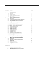
CHAPTER
TITLE
PAGE
1
1.1
1.2
1.3
1.4
INTRODUCTION
Overview
Manual Structure
Module Operational Description
Specifications
1-1
1-2
1-3
1-4
2.1
2.2
2.3
2.4
2.5
2.5.1
2.5.1.1
2.5.1.2
2.5.1.3
2.5.2
2.5.3
2.5.4
2.5.5
2.5.6
2.5.7
2.5.8
2.5.9
2.5.9.1
2.5.9.2
2.5.9.3
2.6
XVME-113 INSTALLATION
Introduction
Location of Components Relevant to Installation
Installing Memory Chips on the XVME-113
Jumper and Switch List
Jumper and Switch Descriptions
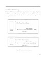
Bank 1 and Bank 2 Address Select
Extended/Standard Select
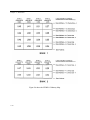
Bank 1 and Bank 2 Addressing Boundaries
Bank 1 Address Configuration Example
Address Modifier Decode
Memory Device Speed
Memory Device Type
Memory Device Size
Memory Backup Power
SYSRESET* Driver
SYSFAIL* Driver
Addressing of RTC/Configuration Port
RTC/Configuration Port Enable/Disable
VMEbus Options
Supervisory/Non-Privilidged Mode Selection
Installing the XVME-113 into a Cardcage
2-1
2-1
2-3
2-4
2-5
2-5
2-5
2-9
2-11
2-11
2-13
2-14
2-17
2-18
2-19
2-20
2-21
2-21
2-21
2-24
2-24
2
3
3.1
3.2
3.3
3.4
3.5
REAL TIME CLOCK PROGRAMMING
Introduction
Real Time Clock/Readable Bank Information
Address Map
Register Map
Register Descriptions
Programming Procedures
3-1
3-2
3-3
3-5
3-9
APPENDICES
A
B
C
VMEbus Connector/Pin Description
Quick Reference Guide
Block Diagram/Assembly Drawing/Schematics
2-iii