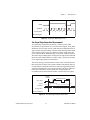
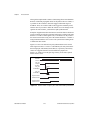
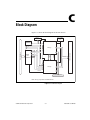
1
DAQ
6601/6602 User Manual
High-Speed Counter/Timer
for PCI or PXI ™ Bus Systems
6601/6602 User Manual
January 1999 Edition
Part Number 322137B-01
Worldwide Technical Support and Product Information
http://www.natinst.com
National Instruments Corporate Headquarters
11500 North Mopac Expressway
Austin, Texas 78759-3504
USA Tel: 512 794 0100
Worldwide Offices
Australia 03 9879 5166, Austria 0662 45 79 90 0, Belgium 02 757 00 20, Brazil 011 284 5011,
Canada (Ontario) 905 694 0085, Canada (Québec) 514 694 8521, Denmark 45 76 26 00, Finland 09 725 725 11,
France 0 1 48 14 24 24, Germany 089 741 31 30, Hong Kong 2645 3186, India 91805275406,
Israel 03 6120092, Italy 02 413091, Japan 03 5472 2970, Korea 02 596 7456, Mexico (D.F.) 5 280 7625,
Mexico (Monterrey) 8 357 7695, Netherlands 0348 433466, Norway 32 84 84 00, Singapore 2265886,
Spain (Madrid) 91 640 0085, Spain (Barcelona) 93 582 0251, Sweden 08 587 895 00,
Switzerland 056 200 51 51, Taiwan 02 2377 1200, United Kingdom 01635 523545
For further support information, see the Technical Support Resources appendix of this manual.
© Copyright 1999 National Instruments Corporation. All rights reserved.
Important Information
Warranty
The PCI-6601, PCI-6602, and PXI-6602 are warranted against defects in materials and workmanship for a period of
one year from the date of shipment, as evidenced by receipts or other documentation. National Instruments will, at its
option, repair or replace equipment that proves to be defective during the warranty period. This warranty includes parts
and labor.
The media on which you receive National Instruments software are warranted not to fail to execute programming
instructions, due to defects in materials and workmanship, for a period of 90 days from date of shipment, as evidenced
by receipts or other documentation. National Instruments will, at its option, repair or replace software media that do not
execute programming instructions if National Instruments receives notice of such defects during the warranty period.
National Instruments does not warrant that the operation of the software shall be uninterrupted or error free.
A Return Material Authorization (RMA) number must be obtained from the factory and clearly marked on the outside
of the package before any equipment will be accepted for warranty work. National Instruments will pay the shipping costs
of returning to the owner parts which are covered by warranty.
National Instruments believes that the information in this document is accurate. The document has been carefully
reviewed for technical accuracy. In the event that technical or typographical errors exist, National Instruments reserves
the right to make changes to subsequent editions of this document without prior notice to holders of this edition. The
reader should consult National Instruments if errors are suspected. In no event shall National Instruments be liable for
any damages arising out of or related to this document or the information contained in it.
EXCEPT AS SPECIFIED HEREIN, NATIONAL INSTRUMENTS MAKES NO WARRANTIES, EXPRESS OR IMPLIED, AND SPECIFICALLY DISCLAIMS
ANY WARRANTY OF MERCHANTABILITY OR FITNESS FOR A PARTICULAR PURPOSE. CUSTOMER’S RIGHT TO RECOVER DAMAGES CAUSED
BY FAULT OR NEGLIGENCE ON THE PART OF NATIONAL INSTRUMENTS SHALL BE LIMITED TO THE AMOUNT THERETOFORE PAID BY THE
CUSTOMER. NATIONAL INSTRUMENTS WILL NOT BE LIABLE FOR DAMAGES RESULTING FROM LOSS OF DATA, PROFITS, USE OF PRODUCTS,
OR INCIDENTAL OR CONSEQUENTIAL DAMAGES, EVEN IF ADVISED OF THE POSSIBILITY THEREOF. This limitation of the liability of
National Instruments will apply regardless of the form of action, whether in contract or tort, including negligence.
Any action against National Instruments must be brought within one year after the cause of action accrues. National
Instruments shall not be liable for any delay in performance due to causes beyond its reasonable control. The warranty
provided herein does not cover damages, defects, malfunctions, or service failures caused by owner’s failure to follow
the National Instruments installation, operation, or maintenance instructions; owner’s modification of the product;
owner’s abuse, misuse, or negligent acts; and power failure or surges, fire, flood, accident, actions of third parties,
or other events outside reasonable control.
Copyright
Under the copyright laws, this publication may not be reproduced or transmitted in any form, electronic or mechanical,
including photocopying, recording, storing in an information retrieval system, or translating, in whole or in part, without
the prior written consent of National Instruments Corporation.
Trademarks
ComponentWorks™, CVI™, DAQCard™, DAQPad™, LabVIEW™, MITE™, natinst.com™, NI-DAQ™, PXI™, RTSI™,
SCXI™, and VirtualBench™ are trademarks of National Instruments Corporation.
Product and company names mentioned herein are trademarks or trade names of their respective companies.
WARNING REGARDING MEDICAL AND CLINICAL USE OF NATIONAL INSTRUMENTS PRODUCTS
National Instruments products are not designed with components and testing for a level of reliability suitable for use in
or in connection with surgical implants or as critical components in any life support systems whose failure to perform
can reasonably be expected to cause significant injury to a human. Applications of National Instruments products
involving medical or clinical treatment can create a potential for death or bodily injury caused by product failure, or by
errors on the part of the user or application designer. Because each end-user system is customized and differs from
National Instruments testing platforms and because a user or application designer may use National Instruments products
in combination with other products in a manner not evaluated or contemplated by National Instruments, the user or
application designer is ultimately responsible for verifying and validating the suitability of National Instruments products
whenever National Instruments products are incorporated in a system or application, including, without limitation,
the appropriate design, process and safety level of such system or application.
Contents
About This Manual
How to Use the Manual Set ...........................................................................................xi
Conventions Used in This Manual.................................................................................xii
Related Documentation..................................................................................................xii
Chapter 1
Introduction
About the 660x Devices.................................................................................................1-1
Using PXI with CompactPCI.........................................................................................1-1
What You Need to Get Started ......................................................................................1-2
Unpacking ......................................................................................................................1-3
Software Programming Choices ....................................................................................1-3
National Instruments Application Software ....................................................1-4
NI-DAQ Driver Software ................................................................................1-4
Optional Equipment .......................................................................................................1-6
Chapter 2
Installation and Configuration
Software Installation ......................................................................................................2-1
Hardware Installation.....................................................................................................2-1
Device Configuration.....................................................................................................2-3
Chapter 3
Device Overview
Device Description ........................................................................................................3-1
Functionality ..................................................................................................................3-3
Counter Applications.......................................................................................3-3
Simple Counting and Time Measurement.......................................................3-4
Event Counting .................................................................................3-4
Simple Event Counting.......................................................3-4
Gated-Event Counting ........................................................3-5
Time Measurement ...........................................................................3-5
Single-Period Measurement ...............................................3-6
Single Pulse-Width Measurement ......................................3-6
Two-Signal Edge-Separation Measurement .......................3-7
© National Instruments Corporation
v
6601/6602 User Manual
Contents
Simple Pulse and Pulse-Train Generation ...................................................... 3-8
Simple Pulse Generation .................................................................. 3-8
Single Pulse Generation ..................................................... 3-8
Single-Triggered Pulse Generation .................................... 3-9
Retriggerable Single Pulse Generation .............................. 3-9
Pulse-Train Generation..................................................................... 3-10
Continuous Pulse-Train Generation ................................... 3-10
Frequency Shift Keying (FSK) .......................................... 3-11
Buffered Counting and Time Measurements .................................................. 3-11
Buffered Event Counting.................................................................. 3-11
Buffered Period Measurement.......................................................... 3-12
Buffered Semiperiod Measurement.................................................. 3-13
Buffered Pulse-Width Measurement ................................................ 3-13
Buffered Two-Signal Edge-Separation Measurement...................... 3-14
Other Counter Applications ............................................................................ 3-15
Pulse Generation for ETS ................................................................. 3-15
Buffered Periodic Event Counting ................................................... 3-16
Frequency Measurement................................................................... 3-16
Buffered Frequency Measurement ................................................... 3-17
Finite Pulse-Train Generation .......................................................... 3-17
Frequency Division........................................................................... 3-18
Reciprocal Frequency Measurement ................................................ 3-18
Position Measurement..................................................................................... 3-18
Quadrature Encoders ........................................................................ 3-18
Two-Pulse Encoders ......................................................................... 3-21
Miscellaneous Functions................................................................................. 3-21
Filters ................................................................................................ 3-21
Flexible Period and Frequency Measurements................................. 3-23
Digital I/O......................................................................................... 3-26
Prescaling.......................................................................................... 3-26
Simultaneous Arming of Counters ................................................... 3-27
Pad Synchronization ......................................................................... 3-27
Synchronous Counting Mode ........................................................... 3-29
When Synchronous Counting Mode Should Be Used ....... 3-30
When Synchronous Counting Should Not Be Used........... 3-31
Transfer Rates................................................................................................................ 3-32
6601/6602 User Manual
vi
© National Instruments Corporation
Contents
Chapter 4
Signal Connections
I/O Connector ................................................................................................................4-1
Output on Counter Pins ...................................................................................4-10
Counter Input Selections .................................................................................4-12
Signal Characteristics ......................................................................................4-17
RTSI Bus Interface ..........................................................................................4-17
Board and RTSI Clocks ....................................................................4-18
RTSI Triggers ...................................................................................4-18
Pull-Up and Pull-Down Connections ............................................................................4-19
Power Connections ........................................................................................................4-19
Field Wiring and Termination .......................................................................................4-19
Transmission Line Effects .............................................................................................4-20
Noise ..............................................................................................................................4-21
Crosstalk ........................................................................................................................4-21
Inductive Effects ............................................................................................................4-22
Appendix A
Specifications
Appendix B
Timing Specifications
Appendix C
Block Diagram
Appendix D
Technical Support Resources
Glossary
Index
© National Instruments Corporation
vii
6601/6602 User Manual
Contents
Figures
Figure 1-1.
The Relationship between the Programming Environment,
NI-DAQ, and Your Hardware............................................................... 1-5
Figure 3-1.
Figure 3-2.
Figure 3-3.
Figure 3-4.
Figure 3-5.
Figure 3-6.
Figure 3-7.
Figure 3-8.
Figure 3-9.
Figure 3-10.
Figure 3-11.
Figure 3-12.
Figure 3-13.
Figure 3-14.
Figure 3-15.
Figure 3-16.
Figure 3-17.
Figure 3-18.
Figure 3-19.
Figure 3-20.
Figure 3-21.
Figure 3-22.
Figure 3-23.
Figure 3-24.
Figure 3-25.
Figure 3-26.
Figure 3-27.
Figure 3-28.
Figure 3-29.
Figure 3-30.
Figure 3-31.
Simple Event Counting ......................................................................... 3-5
Gated-Event Counting .......................................................................... 3-5
Single-Period Measurement.................................................................. 3-6
Single Pulse-Width Measurement......................................................... 3-7
Two-Signal Edge-Separation Measurement ......................................... 3-7
Output Modes........................................................................................ 3-8
Single Pulse Generation ........................................................................ 3-9
Single-Triggered Pulse Generation....................................................... 3-9
Retriggerable Single Pulse Generation ................................................. 3-10
Continuous Pulse-Train Generation...................................................... 3-10
Frequency Shift Keying ........................................................................ 3-11
Buffered Event Counting ...................................................................... 3-12
Buffered Period Measurement .............................................................. 3-12
Buffered Semiperiod Measurement ...................................................... 3-13
Buffered Pulse-Width Measurement..................................................... 3-14
Buffered Two-Signal Edge-Separation Measurement .......................... 3-14
Pulse Generation for ETS ..................................................................... 3-15
Buffered Periodic Event Counting........................................................ 3-16
Frequency Measurement ....................................................................... 3-16
Buffered Frequency Measurement........................................................ 3-17
Finite Pulse-Train Generation............................................................... 3-17
Frequency Division ............................................................................... 3-18
Reciprocal Frequency Measurement..................................................... 3-18
Position Measurement for X1 Encoders ............................................... 3-19
Position Measurement for X2 Encoders ............................................... 3-19
Position Measurement for X4 Encoders ............................................... 3-19
Channel Z Reload ................................................................................. 3-20
Two-Pulse Encoders ............................................................................. 3-21
Filters .................................................................................................... 3-22
Counter 1 Used for Frequency and Period Measurements ................... 3-25
Counters 0 and 1 Used for Frequency and Period
Measurements Simultaneously ............................................................. 3-26
Prescaling .............................................................................................. 3-27
Counters 0 and 1 Using PFI_38 as Gate without
Pad Synchronization ............................................................................. 3-28
Counters 0 and 1 Using PFI_38 as Gate with
Pad Synchronization ............................................................................. 3-29
Without Synchronous Counting Mode ................................................. 3-30
With Synchronous Counting Mode ...................................................... 3-30
Figure 3-32.
Figure 3-33.
Figure 3-34.
Figure 3-35.
Figure 3-36.
6601/6602 User Manual
viii
© National Instruments Corporation
Contents
Figure 4-1.
Figure 4-9.
Figure 4-10.
Figure 4-11.
Figure 4-12.
Comprehensive Description of PFI Line Functionality
for 6601 Devices ...................................................................................4-2
Description of PFI Lines for Counter Applications
for 6601 Devices ...................................................................................4-3
Description of PFI Lines for Motion Encoder Applications
for 6601 Devices ...................................................................................4-4
Description of PFI Lines for DIO Applications
for 6601 Devices ...................................................................................4-5
Comprehensive Description of PFI Line Functionality
for 6602 Devices ...................................................................................4-6
Description of PFI Lines for Counter Applications
for 6602 Devices ...................................................................................4-7
Description of PFI Lines for Motion Encoder Applications
for 6602 Devices ...................................................................................4-8
Description of PFI Lines for DIO Applications
for 6602 Devices ...................................................................................4-9
Counter Input.........................................................................................4-12
Parallel and Series Termination ............................................................4-20
Crosstalk................................................................................................4-21
Wiring to Minimize Inductive Effects...................................................4-22
Figure B-1.
Figure B-2.
Figure B-3.
Counter SOURCE Minimum Period and Minimum Pulse Width ........B-1
Counter GATE Minimum Pulse Width.................................................B-2
Counter Source to Counter Out Timing ................................................B-3
Figure C-1.
660x Block Diagram..............................................................................C-1
Figure 4-2.
Figure 4-3.
Figure 4-4.
Figure 4-5.
Figure 4-6.
Figure 4-7.
Figure 4-8.
Tables
Table 1-1.
Pins Used by the PXI-6602 Device.......................................................1-2
Table 3-1.
Table 3-2.
Table 3-3.
Counter-Based Applications .................................................................3-3
Properties of the Different Filter Settings .............................................3-23
Period Measurements ............................................................................3-23
Table 4-1.
Table 4-2.
Table 4-3.
Table 4-4.
Signals That Can Be Driven onto the PFI Lines ..................................4-10
Possible Selections for Counter Input ..................................................4-13
Signals That Can Be Driven onto the RTSI Bus ...................................4-18
Pin Number of Associated GND on 68-Pin Connector Block .............4-23
Table B-1.
Table B-2.
Table B-3.
Counter SOURCE Minimum Period and Minimum Pulse Width ........B-1
Counter GATE Minimum Pulse Width.................................................B-2
Counter Source to Counter Out Timing ................................................B-3
© National Instruments Corporation
ix
6601/6602 User Manual
About This Manual
This manual describes the electrical and mechanical aspects of
660x devices, and contains information concerning their operation and
programming. Unless otherwise noted, text applies to each 660x device, the
PCI-6601, PCI-6602, and PXI-6602. The PCI and PXI implementations are
the same in functionality; their primary difference is the bus interface.
How to Use the Manual Set
The 6601/6602 User Manual is one piece of the documentation set for your
data acquisition (DAQ) system. You could have any of several types of
documentation, depending on the hardware and software in your system.
Use the different types of documentation you have as follows:
•
Your DAQ hardware user manuals—These manuals have detailed
information about the DAQ hardware that plugs into or is connected to
your computer. Use these manuals for hardware installation and
configuration instructions, specification information about your DAQ
hardware, and application hints.
•
Software documentation—Examples of software documentation you
may have are the LabVIEW, LabWindows/CVI, and NI-DAQ
documentation. After you set up your hardware system, use either the
application software or the NI-DAQ documentation to help you write
your application. If you have a large, complicated system, it is
worthwhile to look through the software documentation before you
configure your hardware.
•
Accessory installation guides or manuals—If you are using accessory
products, read the terminal block and cable assembly installation
guides or accessory board user manuals. They explain how to
physically connect the relevant pieces of the system. Consult these
guides when you are making your connections.
© National Instruments Corporation
xi
6601/6602 User Manual
About This Manual
Conventions
The following conventions are used in this manual:
<>
Angle brackets containing numbers separated by an ellipsis represent a
range of values associated with a bit or signal name (for example,
DIO<0..7>).
6601 device
Refers to the PCI-6601.
6602 device
Refers to the PCI-6602 and PXI-6602, unless otherwise noted.
660x device
Refers to the PCI-6601, PCI-6602, and PXI-6602, unless otherwise noted.
PCI-660x device
Refers to the PCI-6601 and PCI-6602, unless otherwise noted.
♦
The ♦ symbol indicates that the text following it applies only to a specific
660x device.
This icon to the left of bold italicized text denotes a note, which alerts you
to important information.
!
This icon to the left of bold italicized text denotes a caution, which advises
you of precautions to take to avoid injury, data loss, or a system crash.
bold
Bold text denotes the names of menus, menu items, parameters, dialog
boxes, dialog box buttons or options, icons, windows, Windows 95/98/NT
tabs, or LEDs.
bold italic
Bold italic text denotes a note, caution, or warning.
italic
Italic text denotes emphasis, a cross reference, or an introduction to a key
concept.
The Glossary lists abbreviations, acronyms, definitions, metric prefixes,
mnemonics, symbols, and terms.
Related Documentation
The following documents contain information that you may find helpful as
you read this manual:
6601/6602 User Manual
•
Your computer’s technical reference manual
•
National Instruments PXI Specification, rev. 1.0
•
PICMG CompactPCI 2.0 R2.1 core specification
xii
© National Instruments Corporation
1
Introduction
This chapter describes the 660x devices, lists what you need to get started,
describes optional equipment, and explains how to unpack your device.
About the 660x Devices
Thank you for buying a National Instruments 660x device. The
660x devices are timing and digital I/O boards for use with the PCI bus in
PC-compatible computers, or PXI or compactPCI chassis. The
6601 devices offer four 32-bit counter channels and up to 32 lines of
individually configurable, TTL/CMOS-compatible digital I/O. The 6602
devices offer this capability plus four additional 32-bit counter channels.
The counter/timer channels have many measurement and generation modes
such as event counting, time measurement, frequency measurement,
encoder position measurement, pulse generation, and square-wave
generation.
The 660x devices contain the National Instruments MITE PCI interface.
The MITE offers bus-master operation, PCI burst transfers, and high-speed
DMA controller(s) for continuous, scatter-gather DMA without requiring
DMA resources from your computer. See the Using PXI with CompactPCI
section in this chapter for more information on your PXI-6602 device.
For information on device functionality, see Chapter 3, Device Overview.
For detailed 660x device specifications, see Appendix A, Specifications.
Using PXI with CompactPCI
Using PXI-compatible products with standard CompactPCI products is an
important feature provided by the PXI Specification, rev. 1.0. If you use a
PXI-compatible plug-in device in a standard CompactPCI chassis, you will
be unable to use PXI-specific functions, but you can still use the basic
plug-in device functions. For example, the RTSI bus on your PXI-6602
device is available in a PXI chassis, but not in a CompactPCI chassis.
© National Instruments Corporation
1-1
6601/6602 User Manual
Chapter 1
Introduction
The CompactPCI specification permits vendors to develop sub-buses that
coexist with the basic PCI interface on the CompactPCI bus. Compatible
operation is not guaranteed between CompactPCI devices with different
sub-buses nor between CompactPCI devices with sub-buses and PXI. The
standard implementation for CompactPCI does not include these
sub-buses. Your PXI-6602 device will work in any standard CompactPCI
chassis adhering to the PICMG CompactPCI 2.0 R2.1 specification.
PXI specific features are implemented on the J2 connector of the
CompactPCI bus. Table 1-1 lists the J2 pins used by your PXI-6602 device.
Your PXI device is compatible with any CompactPCI chassis with a
sub-bus that does not drive these lines. Even if the sub-bus is capable of
driving these lines, the PXI device is still compatible as long as those pins
on the sub-bus are disabled by default and not ever enabled. Damage may
result if these lines are driven by the sub-bus.
Table 1-1. Pins Used by the PXI-6602 Device
PXI-6602 Signal
PXI Pin Name
PXI J2 Pin Number
RTSI Trigger
(0..5)
PXI Trigger (0..5)
B16, A16, A17, A18, B18,
C18
RTSI Trigger (6)
PXI Star
D17
RTSI Clock
PXI Trigger (7)
E16
Reserved
LBR (7, 8, 10, 11,
12)
A3, C3, E3, A2, B2
What You Need to Get Started
To set up and use your 660x device, you will need the following:
❑ One of the following devices:
•
PCI-6601
•
PCI-6602
•
PXI-6602
❑ 6601/6602 User Manual
6601/6602 User Manual
1-2
© National Instruments Corporation
Chapter 1
Introduction
❑ One of the following software packages and documentation:
•
NI-DAQ for PC compatibles
•
LabVIEW for Windows
•
LabWindows/CVI
❑ Shielded (SH68-68-D1) or ribbon (R6868) cable
❑ SCB-68, TBX-68, or CB-68LP connector block
❑ Your computer, or a PXI or CompactPCI chassis and controller
Unpacking
Your 660x device is shipped in an antistatic package to prevent electrostatic
damage to the device. Electrostatic discharge can damage several
components on the device. To avoid such damage in handling the device,
take the following precautions:
•
Ground yourself via a grounding strap or by holding a grounded object.
•
Touch the antistatic package to a metal part of your computer chassis
before removing the device from the package.
•
Remove the device from the package and inspect the device for loose
components or any sign of damage. Notify National Instruments if the
device appears damaged in any way. Do not install a damaged device
in your computer.
•
Never touch the exposed pins of connectors.
Store your 660x device in the antistatic envelope when not in use.
Software Programming Choices
There are several options to choose from when programming your National
Instruments DAQ hardware. You can use LabVIEW, LabWindows/CVI, or
NI-DAQ.
© National Instruments Corporation
1-3
6601/6602 User Manual
Chapter 1
Introduction
National Instruments Application Software
LabVIEW features interactive graphics, a state-of-the art user interface,
and a powerful graphical programming language. The LabVIEW Data
Acquisition VI Library, a series of virtual instruments (VIs) for using
LabVIEW with National Instruments DAQ hardware, is included with
LabVIEW. The LabVIEW Data Acquisition VI Library is functionally
equivalent to the NI-DAQ software.
LabWindows/CVI features interactive graphics and a state-of-the-art user
interface, and uses the ANSI standard C programming language. The
LabWindows/CVI Data Acquisition Library, a series of functions for using
National Instruments DAQ hardware, is included with LabWindows/CVI.
The LabWindows/CVI Data Acquisition Library is functionally equivalent
to the NI-DAQ software.
Using LabVIEW or LabWindows/CVI software will greatly reduce the
development time for your data acquisition and control application.
NI-DAQ Driver Software
The NI-DAQ driver software is included at no charge with all National
Instruments DAQ hardware. NI-DAQ has an extensive library of functions
that you can call from your application programming environment. These
functions include routines for digital I/O, counter/timer operations, RTSI,
and acquiring data to extended memory.
NI-DAQ has both high-level DAQ I/O functions for maximum ease of use
and low-level DAQ I/O functions for maximum flexibility and
performance. Examples for high-level functions are streaming data to disk
or acquiring a certain number of data points. An example of a low-level
function is writing directly to registers on the DAQ device. NI-DAQ does
not sacrifice performance of National Instruments DAQ devices because it
lets multiple devices operate at their peak performance, even
simultaneously.
6601/6602 User Manual
1-4
© National Instruments Corporation
Chapter 1
Introduction
NI-DAQ also internally addresses many of the complex issues between the
computer and the DAQ hardware such as programming interrupts and
DMA controllers. NI-DAQ maintains a consistent software interface so that
you can change platforms with minimal modifications to your code.
Whether you are using conventional programming languages or NI-DAQ
software, your application uses the NI-DAQ driver software, as illustrated
in Figure 1-1.
ComponentWorks,
LabVIEW,
LabWindows/CVI,
or VirtualBench
Conventional
Programming
Environment
NI-DAQ
Driver Software
DAQ or
SCXI Hardware
Personal
Computer or
Workstation
Figure 1-1. The Relationship between the Programming Environment, NI-DAQ,
and Your Hardware
You can use your 660x device, together with other AT (16-bit ISA), PCI,
PC, EISA, DAQCard, and DAQPad Series DAQ hardware, with NI-DAQ
software for PC compatibles. The PCI-6602 and PXI-6602 require
version 6.5 or later. The PCI-6601 requires version 6.6 or later.
© National Instruments Corporation
1-5
6601/6602 User Manual
Chapter 1
Introduction
Optional Equipment
National Instruments offers the following accessories to use with your
660x device:
•
Shielded and unshielded 68-pin cables and screw terminals
•
Real Time System Integration (RTSI) bus cables
For more specific information about these products, refer to the National
Instruments catalogue or web site, or call the office nearest you.
6601/6602 User Manual
1-6
© National Instruments Corporation
Installation and Configuration
2
This chapter explains how to install and configure your 660x device.
Software Installation
Install your software before you install your 660x device. Refer to the
appropriate release notes indicated below for specific instructions on the
software installation sequence.
If you are using NI-DAQ, refer to your NI-DAQ release notes. Find
the installation section for your operating system and follow the
instructions given there.
If you are using LabVIEW, LabWindows/CVI, or other National
Instruments software, refer to the appropriate release notes. After you have
installed your application software, refer to your NI-DAQ release notes and
follow the instructions given there for your operating system and
application software package.
Hardware Installation
Note
Install the software before you install your 660x device.
Following are general installation instructions for each device. Consult
your computer or chassis user manual or technical reference manual for
specific instructions and warnings about installing new devices in your
computer or chassis.
♦
PCI-6601, PCI-6602
You can install a PCI-660x in any available 5 V PCI expansion slot in your
computer.
1.
Turn off and unplug your computer.
2.
Remove the top cover or access port to the expansion slots.
3.
Remove the expansion slot cover on the back panel of the computer.
© National Instruments Corporation
2-1
6601/6602 User Manual
Chapter 2
Installation and Configuration
4.
Touch any metal part of your computer chassis to discharge any static
electricity that might be on your clothes or body.
5.
Insert the PCI-660x into a 5 V PCI slot. It may be a tight fit, but do not
force the device into place.
6.
Screw the mounting bracket of the PCI-660x to the back panel rail of
the computer.
7.
Visually verify the installation.
8.
Replace the top cover of your computer.
9.
Plug in and turn on your computer.
Your PCI-660x is now installed. The device is now ready for software
configuration.
♦
PXI-6602
You can install a PXI-6602 in any available 5 V peripheral slot in your PXI
or CompactPCI chassis.
Note
The PXI-6602 has connections to several reserved lines on the CompactPCI
J2 connector. Before installing a PXI-6602 in a CompactPCI system that uses
J2 connector lines for purposes other than PXI, see the Using PXI with
CompactPCI section in Chapter 1, Introduction.
1.
Turn off and unplug your PXI or CompactPCI chassis.
2.
Choose an unused PXI or CompactPCI 5 V peripheral slot. For
maximum performance when using a non-PXI chassis, install the
PXI-6602 in a slot that supports bus arbitration or bus-master cards.
The PXI-6602 contains onboard bus-master DMA logic that can
operate only in such a slot. If you choose a slot that does not support
bus masters, you will have to disable the onboard DMA controller
using your software. PXI-compliant chassis must have bus arbitration
for all slots.
3.
Remove the filler panel for the peripheral slot you have chosen.
4.
Touch a metal part on your chassis to discharge any static electricity
that might be on your clothes or body.
5.
Insert the PXI-6602 in the selected 5 V slot. Use the injector/ejector
handle to fully inject the device into place.
6.
Screw the front panel of the PXI-6602 to the front panel mounting rails
of the PXI or CompactPCI chassis.
7.
Visually verify the installation.
8.
Plug in and turn on the PXI or CompactPCI chassis.
Your PXI-6602 is now installed. You are now ready to configure your
hardware and software.
6601/6602 User Manual
2-2
© National Instruments Corporation
Chapter 2
Installation and Configuration
Device Configuration
Each 660x device is completely software configurable. The system
software automatically allocates all device resources, including base
memory address and interrupt level. These devices do not require DMA
controller resources from your computer. You must assign a device number
to your 660x device. Double-click on the Measurement & Automation
icon—placed on your Windows desktop by NI-DAQ—to assign a device
number to your device. The Measurement & Automation Explorer has
online help if you need more information on how to assign a device
number. Refer to device configuration instructions in your NI-DAQ
documents and online help.
© National Instruments Corporation
2-3
6601/6602 User Manual
3
Device Overview
This chapter provides an overview of the hardware functions of your
660x device.
Device Description
Each 660x device is a completely switchless, jumperless device and
requires only software configuration. The 660x devices derive most of their
functionality from the NI-TIO, a sophisticated, state-of-the-art counter and
digital I/O ASIC developed by National Instruments. A 6601 device has
one NI-TIO and offers four 32-bit up/down counters with prescalers. Each
6602 device has two NI-TIOs and offers eight such counters (see
Appendix C, Block Diagram, for the architecture of a 660x device). The
counters on 660x devices are a superset of the general-purpose counters on
the DAQ-STC. The DAQ-STC counters are used on all National
Instruments E Series devices.
The 660x counters offer backward compatibility with the DAQ-STC with
regard to functionality and software programming. The same software API
and functions are used to program the DAQ-STC general-purpose counters
and the counters on the 660x devices. Because of greater resources and
added functionality, new constants, parameters, and functions have been
created for 660x counters. However, new functions exist to provide new
functionality only—they will not affect code written for the DAQ-STC
counters. In most cases, code written for the DAQ-STC general-purpose
counters will work for the 660x counters.
The few changes needed within the National Instruments API are mostly
due to different constants for I/O connector signals (PFI lines). For
example, E Series devices can select any of PFI <0..9> as a source for the
general-purpose counters. For 660x devices, the corresponding choices
include PFI_39, PFI_35, and so on.
© National Instruments Corporation
3-1
6601/6602 User Manual
Chapter 3
Device Overview
The counters on the 6601 device have two internal timebases: 100 kHz and
20 MHz. The counters on the 6602 devices have three internal timebases:
100 kHz, 20 MHz, and 80 MHz. Each counter has a gate, up/down, and
source input. Each of these inputs can be an internal signal or an external
signal that connects to the I/O connector. Each counter has an output signal
that can provide output in two different modes: toggled output mode and
pulsed output mode. For more information about these modes, refer to the
Simple Pulse Generation section later in this chapter.
In addition, the NI-TIO provides the 660x device with a 32-bit digital I/O
(DIO) port. You can individually configure each line on this port for input
or output and perform a read or a write upon a software command. Eight of
these 32 lines are always available for DIO. The remaining 24 lines are
shared with counters. You can configure these 24 lines for counter output
or DIO output on an individual basis. You do not need to specify whether
you are using the line for a counter application or for DIO if you are using
it as an input.
Equipped with the NI-TIO, 660x devices also have other useful functions
such as the ability to decode signals from motion encoders, and digital
filtering on each line from the I/O connector.
With 660x devices, you can use your computer or chassis as a counter/timer
that acts as a system timing controller or measurement instrument for
laboratory testing, production testing, and industrial process monitoring
and control.
6601/6602 User Manual
3-2
© National Instruments Corporation
Chapter 3
Device Overview
Functionality
This section describes the 660x counter applications and other
miscellaneous functions offered by these devices.
Counter Applications
You can use the 660x device in the counter-based applications listed in
Table 3-1. Following the table are detailed descriptions of each application.
Table 3-1. Counter-Based Applications
Application Class
Application
Simple Counting and
Time Measurement
Simple event counting
Gated-event counting
Single-period measurement
Single pulse-width measurement
Two-signal edge-separation measurement
Simple Pulse and
Pulse-Train Generation
Single pulse generation
Single-triggered pulse generation
Retriggerable single pulse generation
Continuous pulse-train generation
Frequency shift keying (FSK)
Buffered Counting and
Time Measurement
Buffered event counting (continuous)
Buffered period measurement (continuous)
Buffered semiperiod measurement (continuous)
Buffered pulse-width measurement (continuous)
Buffered two-signal edge-separation measurement (continuous)
Other Counter
Applications
Pulse generation for Equivalent Time Sampling (ETS)
Buffered periodic event counting (continuous)
Frequency measurement
Buffered frequency measurement (continuous)
Finite pulse-train generation
Frequency division
Reciprocal frequency measurement
© National Instruments Corporation
3-3
6601/6602 User Manual
Chapter 3
Device Overview
Table 3-1. Counter-Based Applications (Continued)
Application Class
Application
Position Measurement
Quadrature encoders
Two-pulse encoders
Miscellaneous Functions
Filters
Flexible period and frequency measurements
Digital I/O
Prescaling
Simultaneous arming of counters
Pad synchronization
Synchronous counting mode
Simple Counting and Time Measurement
Event Counting
In the event-counting functions, the counter counts events on the SOURCE
input after the counter has been armed. The counter can be armed via a
software command or upon receiving a start trigger. The start trigger can be
an internal or external signal. The following actions are available in event
counting:
•
SOURCE increments or decrements the counter.
•
GATE may be used to indicate when to start and stop counting
intervals or when to save the counter contents in the save register.
•
UP_DOWN controls the direction of the counting. When configured
for hardware control of counting direction, the counter counts up when
UP_DOWN is high and it counts down when UP_DOWN is low.
Simple Event Counting
In simple event counting, the counter counts the number of pulses that
occur on the SOURCE signal after the counter has been armed. Software
can read the counter contents at any time without disturbing the counting
process. Figure 3-1 shows an example of simple event counting where the
counter counts five events on SOURCE.
6601/6602 User Manual
3-4
© National Instruments Corporation
Chapter 3
Device Overview
Counter Armed
SOURCE
Counter Value
1
0
2
3
4
5
Figure 3-1. Simple Event Counting
Gated-Event Counting
Gated-event counting is similar to simple event counting except that the
counting process is gated; counting is halted and resumed via the GATE
signal. When GATE is active, the counter counts pulses that occur on the
SOURCE signal after the counter has been armed. When GATE is inactive,
the counter retains the current count value. Figure 3-2 shows an example of
gated-event counting where the gate action allows the counter to count only
five of the pulses on SOURCE.
Counter Armed
GATE
SOURCE
Counter Value
0
0
1
2
3
4
5
Figure 3-2. Gated-Event Counting
Time Measurement
In the time-measurement functions, the counter uses SOURCE as a
timebase to measure the time interval between events on the GATE signal.
The following actions are available in time measurement:
•
Rising edges on SOURCE can increment or decrement the counter
during the measurement interval. Typically, SOURCE is chosen to be
an internal timebase and causes the counter to increment.
•
Counting can begin and end on any two of the GATE edges—active,
inactive, or either.
•
The HW Save register can save the counter value upon the completion
of the measurement.
© National Instruments Corporation
3-5
6601/6602 User Manual
Chapter 3
Device Overview
Single-Period Measurement
In single-period measurement, the counter uses SOURCE to measure the
period of the signal present on the GATE input. The counter counts the
number of rising edges that occur on SOURCE between two active edges
of GATE. At the completion of the period interval for GATE, the HW Save
register latches the counter value for the software read. Figure 3-3 shows a
single-period measurement where the period of GATE is five SOURCE
rising edges.
GATE
SOURCE
0
Counter Value
1
2
3
4
5
5
HW Save Register
Figure 3-3. Single-Period Measurement
Single Pulse-Width Measurement
In single pulse-width measurement, the counter uses SOURCE to measure
the pulse width of the signal present on the GATE input. The counter
counts the number of rising edges that occur on SOURCE while the GATE
signal remains in an active state. At the completion of the pulse-width
interval for GATE, the HW Save register latches the counter value for
software read. Figure 3-4 shows a single pulse-width measurement where
the pulse width of GATE is five SOURCE rising edges.
Note
A pulse width measurement will be accurate even if the counter is armed while a
pulse train is in progress. If a counter is armed while the pulse is in the active state,
it will wait for the next transition to the active state for the measurement.
6601/6602 User Manual
3-6
© National Instruments Corporation
Chapter 3
Device Overview
GATE
SOURCE
0
Counter Value
1
2
3
5
4
5
HW Save Register
Figure 3-4. Single Pulse-Width Measurement
Two-Signal Edge-Separation Measurement
Two-signal edge-separation measurement is similar to pulse-width
measurement, except that there are two measurement signals: AUX_LINE
and GATE. An active edge on AUX_LINE starts the counting and an active
edge on GATE stops the counting. After the counter has been armed and an
active edge has occurred on AUX_LINE, the counter counts pulses that
occur on the SOURCE. Additional edges on the AUX_LINE are ignored.
The counter stops counting upon receiving an active edge on the GATE and
latches the value into the HW Save register. Figure 3-5 shows an example
of two-signal edge-separation measurement.
You can use this type of measurement to count events or measure the time
that occurs between edges on two signals. Outside of this manual, this type
of measurement is sometimes referred to as start/stop trigger measurement,
second gate measurement, or A-to-B measurement. The AUX_LINE and
GATE can be internal or external signals. For external signals, the
UP_DOWN pin associated with the counter is used for the AUX_LINE.
Counter
Armed
Measured Interval
AUX_LINE
GATE
SOURCE
Counter Value
0
0
0
0
1
2
3
4
5
6
7
HW Save Register
8
8
8
8
Figure 3-5. Two-Signal Edge-Separation Measurement
© National Instruments Corporation
3-7
6601/6602 User Manual
Chapter 3
Device Overview
Simple Pulse and Pulse-Train Generation
Simple Pulse Generation
In the pulse generation functions, the counter generates a single pulse of a
specified duration after the counter is armed. The following actions are
available in pulse generation:
•
The counter uses SOURCE as a timebase to generate the pulse.
•
The user specifies the pulse parameters in terms of periods of the
SOURCE input.
•
GATE can serve as a trigger signal to generate a pulse after the first
active gate edge, or after each active gate edge.
•
The hardware provides an alternate output mode so that G_OUT
outputs two counter TC pulses, instead of a single long pulse.
Two output modes are available on the 660x counters: toggled output mode
and pulsed output mode. Each time a counter rolls over from either
direction, it generates a pulse known as the terminal count (TC) pulse. In
pulsed mode, this TC pulse is driven onto the output pin.
In toggled mode, the counter output changes state on the SOURCE edge
that follows the assertion of the TC pulse. Figure 3-6 illustrates the two
output modes for a pulse generation with a delay of two and a pulse width
of four.
SOURCE
Pulsed
Output
Mode
Toggled
Output
Mode
Figure 3-6. Output Modes
Single Pulse Generation
The single pulse generation function generates a single pulse with
programmable delay and programmable pulse width after the counter is
armed. The counter uses SOURCE as a timebase to generate the
pulse—you specify the pulse delay and the pulse width in terms of periods
of the SOURCE input. Figure 3-7 shows the generation of a single pulse
with a pulse delay of four and a pulse width of three.
6601/6602 User Manual
3-8
© National Instruments Corporation
Chapter 3
Device Overview
Counter Armed
SOURCE
OUT
Figure 3-7. Single Pulse Generation
Single-Triggered Pulse Generation
Single-triggered pulse generation is similar to single pulse generation
except that GATE provides a trigger function. An active GATE edge after
the counter has been armed causes the counter to generate a single pulse
with programmable delay and programmable pulse width. The counter
ignores subsequent triggers. You specify the programmable parameters in
terms of periods of the SOURCE input. Figure 3-8 shows the generation of
a single pulse with a pulse delay of four and a pulse width of three.
GATE
SOURCE
OUT
Figure 3-8. Single-Triggered Pulse Generation
Retriggerable Single Pulse Generation
This function is similar to single-triggered pulse generation except that the
counter generates a pulse on every active GATE edge after the counter has
been armed. The counter ignores active gate edges that are received while
the pulse generation is in progress. Each pulse, generated upon receiving a
GATE edge, has the same programmable delay and pulse width. You
specify these parameters in terms of periods of the SOURCE input.
Figure 3-9 shows the generation of two pulses with a pulse delay of five
and a pulse width of three.
© National Instruments Corporation
3-9
6601/6602 User Manual
Chapter 3
Device Overview
GATE
SOURCE
OUT
Figure 3-9. Retriggerable Single Pulse Generation
Pulse-Train Generation
In the pulse-train generation functions, the counter generates a continuous
stream of pulses of specified interval and duration after the counter has
been armed. The following actions are available in pulse-train generation:
Note
•
You can specify the pulse parameters in terms of periods of the
SOURCE input.
•
The hardware has an alternate output mode as explained in the Simple
Pulse Generation section.
With a 50% duty cycle pulse train, you double the frequency if you use the pulsed
output mode.
Continuous Pulse-Train Generation
This function generates a train of pulses with programmable frequency and
duty cycle. The counter uses SOURCE as a timebase to generate the pulses.
You specify the programmable parameters in terms of periods of the
SOURCE input. Figure 3-10 shows a pulse train. You can seamlessly
change the frequency and/or duty cycle of the pulse train while the pulse
train is in progress. The rate at which you can change these parameters
depends on your system.
SOURCE
OUT
Figure 3-10. Continuous Pulse-Train Generation
6601/6602 User Manual
3-10
© National Instruments Corporation
Chapter 3
Device Overview
Frequency Shift Keying (FSK)
FSK is similar to pulse-train generation in that the counter generates a train
of pulses. However, in FSK mode, the GATE signal modulates the
frequency and duty cycle of the output train. The counter implements this
modulation by allowing the GATE signal to select from two different sets
of pulse-train parameters. Figure 3-11 shows an example of FSK. When
GATE is low, the counter generates a low-frequency signal with a long
pulse width. When GATE is high, the counter generates a high-frequency
signal with a short pulse width.
GATE
OUT
START
Figure 3-11. Frequency Shift Keying
Buffered Counting and Time Measurements
Buffered measurements are similar to their single measurement
counterparts. However, multiple successive measurements are made. The
result of each measurement is saved in the Hardware Save Register on each
active edge of GATE. A buffered measurement generates a data stream.
This data stream is transferred to your computer via DMA or interrupts.
You can make multiple buffered measurements simultaneously. Up to three
of the data streams thus generated can be transferred via DMA. Interrupts
are used to transfer any additional data streams. These buffered
measurements can be continuous. The maximum transfer rates for these
buffered measurements are system dependent. See the Transfer Rates
section later in this chapter for additional information.
Buffered Event Counting
Buffered event counting is similar to simple event counting except that the
GATE signal indicates when to save the counter value to the HW Save
register. The active GATE edge latches the count value into the HW Save
register. Counting continues uninterrupted regardless of the GATE
activity. Figure 3-12 shows buffered event counting where the GATE
action causes the HW Save register to save the counter contents twice.
© National Instruments Corporation
3-11
6601/6602 User Manual
Chapter 3
Device Overview
Counter Armed
GATE
SOURCE
0
Counter Value
1
2
3
4
5
6
3
7
3
6
Buffer
Figure 3-12. Buffered Event Counting
Buffered Period Measurement
Buffered period measurement is similar to single-period measurement,
except that measurements are taken for multiple successive periods. The
counter measures the period of the signal present on the GATE input by
counting the number of rising edges that occur on SOURCE between each
pair of active edges of GATE. At each active edge of GATE, the HW Save
register latches the counter value for software read. The counter begins to
count when armed, which could occur between GATE edges. Therefore,
the value latched by the first active GATE edge is unreliable and should be
discarded. Figure 3-13 shows two complete periods of a buffered period
measurement where the period is three SOURCE rising edges. Three
values are latched, but the first value should be discarded.
Counter Armed
GATE
SOURCE
Counter Value
Buffer
1
2
1
2
2 (discard)
2
3
1
3
2
2 (discard)
3
3
1
3
2 (discard)
3
3
Figure 3-13. Buffered Period Measurement
6601/6602 User Manual
3-12
© National Instruments Corporation
Chapter 3
Device Overview
Buffered Semiperiod Measurement
Buffered semiperiod measurement is similar to buffered period
measurement, except that successive measurements are taken over every
semiperiod. The counter measures each half-period of the signal present on
the GATE input by counting the number of rising edges that occur on
SOURCE while GATE remains in each state.
At each edge of GATE, the HW Save register latches the count value for
software read. The Counter begins to count when armed, which could occur
between gate edges. Therefore, the value latched by the first gate edge is
unreliable and should be discarded. Figure 3-14 shows three semiperiods of
a buffered semiperiod measurement where the first semiperiod is three
SOURCE rising edges, the second semiperiod is one SOURCE rising edge,
and the final semiperiod is two SOURCE rising edges. Four values are
latched but the first value is ignored. The first valid measurement is made
on the first active phase of the cycle. You specify which phase of the cycle
is the active phase by specifying the GATE polarity. In Figure 3-14, the first
valid measurement is three SOURCE rising edges, which is the second
value latched.
Counter Armed
GATE
SOURCE
0
Counter Value
1
2
2
Buffer
1
2
2
1
3
3
2
3
1
1
2
3
1
1
2
2
2
3
1
2
Figure 3-14. Buffered Semiperiod Measurement
Buffered Pulse-Width Measurement
Buffered pulse-width measurement is similar to single pulse-width
measurement, except that the measurements are taken over multiple
consecutive pulses. The counter measures the pulse width of the signal
present on the GATE input by counting the number of rising edges that
occur on SOURCE while GATE remains in an active state.
At the completion of each pulse-width interval for GATE, the HW Save
register latches the counter value for software read. Figure 3-15 shows two
© National Instruments Corporation
3-13
6601/6602 User Manual
Chapter 3
Device Overview
pulse widths of a buffered pulse-width measurement where the first pulse
width is three SOURCE rising edges and the second pulse width is two
SOURCE rising edges.
Note
The first measurement will be correct even if the pulse train is in progress when
the counter is armed. If the counter is armed while the GATE is in the active state,
the measurement will begin with the next transition into the active state.
GATE
SOURCE
0
Counter Value
1
2
3
1
3
2
3
Buffer
2
3
2
Figure 3-15. Buffered Pulse-Width Measurement
Buffered Two-Signal Edge-Separation Measurement
Buffered two-signal edge-separation measurement is similar to its single
measurement counterpart, except that measurements are taken over
multiple successive periods. The counter counts the number of rising edges
on SOURCE between the active edge of AUX_LINE and the following
active edge of GATE. At each active edge of GATE, the HW Save register
latches the counter value for software read. Figure 3-16 shows three
instances of buffered two-signal edge-separation measurement where the
separation is three SOURCE rising edges.
AUX_LINE
GATE
SOURCE
Counter Value
1
Buffer
2
3
1
3
2
3
1
2
3
3
3
3
3
3
Figure 3-16. Buffered Two-Signal Edge-Separation Measurement
6601/6602 User Manual
3-14
© National Instruments Corporation
Chapter 3
Device Overview
Other Counter Applications
Pulse Generation for ETS
In this application, the counter produces a pulse on the output a specified
delay after an active edge on GATE. After each active edge on GATE, the
counter cumulatively increments the delay between the GATE and the
pulse on the output by a specified amount. Thus, the delay between the
GATE and the pulse produced successively increases.
The increase in the delay value can be between 0 and 255. For instance, if
you specify the increment to be 10, the delay between the active GATE
edge and the pulse on the output will increase by 10 every time a new pulse
is generated.
Suppose you program your counter to generate pulses with a delay of 100
and pulse width of 200 each time it receives a trigger. Furthermore, suppose
you specify the delay increment to be 10. On the first trigger, your pulse
delay will be 100, on the second it will be 110, on the third it will be 120;
the process will repeat in this manner until the counter is disarmed. The
counter ignores any GATE edge that is received while the pulse triggered
by the previous GATE edge is in progress.
The waveform thus produced at the counter’s output can be used to provide
timing for undersampling applications where a digitizing system can
sample repetitive waveforms that are higher in frequency than the Nyquist
frequency of the system. Figure 3-17 shows an example of pulse generation
for ETS; the delay from the trigger to the pulse increases after each
subsequent GATE active edge.
GATE
Counter TC
OUT
D1
D2 = D1 + ∆D
D3 = D1 + 2∆D
Figure 3-17. Pulse Generation for ETS
© National Instruments Corporation
3-15
6601/6602 User Manual
Chapter 3
Device Overview
Buffered Periodic Event Counting
Buffered periodic event counting is similar to simple event counting except
that there are multiple consecutive counting intervals. The GATE signal
indicates the boundary between consecutive counting intervals. The
counter begins to count when it is armed. Each active edge of the GATE
signal latches the count value for the current counting interval into the
HW Save register and reloads the counter with the initial value to begin the
next counting interval. Figure 3-18 shows buffered periodic event
counting. The counter begins to count before the GATE edge for the first
counting interval occurs.
Counter
Armed
GATE
SOURCE
Counter Value
0
1
2
1
2
3
2
1
2
3
1
2
3
Buffer
2
3
3
Figure 3-18. Buffered Periodic Event Counting
Frequency Measurement
For frequency measurement, a pulse of known width or a waveform of
known frequency and duty cycle is applied to the GATE of the counter. The
signal to be measured is applied to the SOURCE of the counter. The
counter counts how many SOURCE edges are received during the gated
interval. The frequency is the number of counts divided by the duration of
GATE in seconds, as shown in Figure 3-19.
Counter
Armed
GATE
SOURCE
Count
Armed
0
0
0
NO
0
0
YES
0
1
2
3
3
3
3
3
3
3
NO
Figure 3-19. Frequency Measurement
6601/6602 User Manual
3-16
© National Instruments Corporation
Chapter 3
Device Overview
Buffered Frequency Measurement
For this measurement, a pulse train of known pulse width is applied to the
GATE of the counter. The signal to be measured is applied to the SOURCE
of the counter. The counter counts how many source edges are received
during each active phase of the pulse train at its GATE. At each inactive
edge of GATE, the HW Save register latches the counter value for software
read. Figure 3-20 shows an example of buffered frequency measurement.
Counter
Armed
GATE
SOURCE
Count
Armed
0
0
0
NO
0
0
0
1
2
3
0
0
1
2
3
0
YES
3
Buffer
3
3
Figure 3-20. Buffered Frequency Measurement
Finite Pulse-Train Generation
In this application, the counter generates a specified number of pulses as
indicated in Figure 3-21. The high and low phase of the pulse train are
programmable. These values are specified in multiples of the timebase that
is used as the SOURCE of the counter. Figure 3-21 shows two pulses with
a pulse delay of two and a pulse width of three. Two counters are used for
this application.
Counter
Armed
SOURCE
Output
Counter Stops
Figure 3-21. Finite Pulse-Train Generation
© National Instruments Corporation
3-17
6601/6602 User Manual
Chapter 3
Device Overview
Frequency Division
In this application, the counter divides the frequency of the signal
connected to its SOURCE input. The divided signal appears on its OUT
terminal. Figure 3-22 shows a frequency division ratio of six.
SOURCE
Output
Figure 3-22. Frequency Division
Reciprocal Frequency Measurement
In this measurement, you must use two counters to determine the
frequency. First, measure the time over an integer number of cycles of the
signal to be measured. Then, divide the total time by the number of cycles
to obtain a value for the period of the signal. The frequency is the inverse
of the period. Figure 3-23 illustrates this measurement. The number of
cycles for the interval measurement is specified to be 10. The period of the
signal is the interval divided by 10.
SOURCE
Interval Measured by Counter
Interval
Over 10
Cycles
Figure 3-23. Reciprocal Frequency Measurement
Position Measurement
The 660x devices can perform position measurements on signals from two
types of motion encoders:
•
Quadrature encoders (X1, X2, and X4 encoding)
•
Two-pulse encoders (also referred to as up/down encoders)
Quadrature Encoders
A quadrature encoder can have up to three channels: channels A, B, and Z.
When channel A leads channel B in a quadrature cycle, the counter
increments. When channel B leads channel A in a quadrature cycle, the
6601/6602 User Manual
3-18
© National Instruments Corporation
Chapter 3
Device Overview
counter decrements. The amount of increments and decrements per cycle
depends on the type of encoding: X1, X2, or X4.
Figure 3-24 shows a quadrature cycle and the resulting increments and
decrements for X1 encoding. When channel A leads channel B, the
increment occurs on the rising edge of channel A. When channel B leads
channel A, the decrement occurs on the falling edge of channel A.
Ch A
Ch B
Counter
Value 5
6
7
7
6
5
Figure 3-24. Position Measurement for X1 Encoders
The same behavior holds for X2 encoding except the counter increments or
decrements on each edge of channel A, depending on which channel leads
the other. Each cycle results in two increments or decrements, as shown in
Figure 3-25.
Ch A
Ch B
Counter
Value 5
6
7
8
9
9
8
7
6
5
Figure 3-25. Position Measurement for X2 Encoders
Similarly, the counter increments or decrements on each edge of
channels A and B for X4 encoding. Whether the counter increments or
decrements depends on which channel leads the other. Each cycle results in
four increments or decrements, as shown in Figure 3-26.
Ch A
Ch B
Counter
Value
5
6
7
8
9
10
11
12
13
13
12
11
10
9
8
7
6
5
Figure 3-26. Position Measurement for X4 Encoders
Some quadrature encoders have a third channel, channel Z, which is also
referred to as the index channel. A high level on channel Z causes the
© National Instruments Corporation
3-19
6601/6602 User Manual
Chapter 3
Device Overview
counter to be reloaded with a specified value in a specified phase of the
quadrature cycle. You can program this reload to occur in any one of the
four phases in a quadrature cycle.
Note
In NI-DAQ version 6.5, channel Z reload can only occur when channels A and B
are both low. The ability to reload in other phases is available in NI-DAQ
version 6.6 or later.
Channel Z behavior—when it goes high and how long it stays high—differs
with quadrature encoder designs. You must refer to the documentation for
your quadrature encoder to obtain timing of channel Z with respect to
channels A and B. You must then ensure that channel Z is high during at
least a portion of the phase you specify for reload. For instance, in
Figure 3-27, channel Z is never high when channel A is high and channel B
is low. Thus, the reload must occur in some other phase.
In Figure 3-27, the reload phase is when both channel A and channel B are
low. The reload occurs when this phase is true and channel Z is high.
Incrementing and decrementing takes priority over reloading. Thus, when
the channel B goes low to enter the reload phase, the increment occurs first.
The reload occurs within one maximum timebase period after the reload
phase becomes true. After the reload occurs, the counter continues to count
as before. Figure 3-27 illustrates channel Z reload with X4 decoding.
Ch A
Ch B
Ch Z
Max
Timebase
Counter
Value
5
6
7
8
9
0
1
2
3
4
A=0
B=0
Z=1
Figure 3-27. Channel Z Reload
6601/6602 User Manual
3-20
© National Instruments Corporation
Chapter 3
Device Overview
Two-Pulse Encoders
Two-pulse encoding supports two channels: channels A and B. A pulse on
channel A causes the counter to increment on its rising edge. A pulse on
channel B causes the counter to decrement on its rising edge, as shown in
Figure 3-28.
Ch A
Ch B
Counter
Value
2
3
4
5
4
3
4
Figure 3-28. Two-Pulse Encoders
Miscellaneous Functions
Filters
Each PFI line coming from the I/O connector can be passed through a
simple digital debouncing filter. The filter operates off a filter clock and a
fast internal sampling clock. The filter circuit samples the signal on the PFI
line on each rising edge of the sampling clock. A change in the signal is
propagated only if it maintains its new state for at least the duration
between two consecutive rising edges of the filter clock. The frequency of
the filter clock determines whether a transition in the signal may propagate
or not. The function of the sampling clock is to increase the sampling rate
and prevent aliasing. Figure 3-29 demonstrates the function of this filter.
In Figure 3-29, the low-to-high transition is guaranteed to be passed
through only if the signal remains high for at least two filter clock periods
and is sampled high at each sampling clock rising edge during this time.
Although the low-to-high transition is shown in this example, the same is
true for high-to-low transitions.
Note
The effect of filtering is that the signal transition is shifted by two filter clock
periods.
© National Instruments Corporation
3-21
6601/6602 User Manual
Chapter 3
Device Overview
External
Signal
On PFI Line
Filter
Clock
Max Time Base
External
Signal
Sample by
Max Time Base
H
L
L
H
H
H
H
H
H
H
Filtered
PFI Line
Figure 3-29. Filters
Figure 3-29 shows that if sampling was done at each rising edge of the filter
clock alone, the first two pulses would have been seen as one continuous
transition. However, using the faster sampling clock detects the glitch; thus,
the two short pulses are ignored.
The intent of the filter is to eliminate glitches that may appear on a signal.
The filter is sensitive to the duration for which a digital signal transitions
from one state to another. Thus, if a square wave is applied to the filter, its
propagation will depend on its frequency and duty cycle.
There are four filter settings available in the 660x devices: 5 µs, 1 µs,
500 ns, and 100 ns. The 5 µs filter will pass all pulse widths (high and low)
that are 5 µs or longer; it will block all pulse widths that are 2.5 µs (one-half
of 5 µs) or shorter. Pulse widths between 2.5 µs and 5 µs may or may not
pass, depending on the phase of the pulse with respect to the filter clock.
The same relationship extends to all other filter clocks.
In addition to these hard-wired filter clocks, you can use the output of any
one of the counters as a filter clock. Configure the counter for pulse-train
generation and use a pulse train with a duty cycle as near 50% as possible.
The output of this counter is then selected as a filter clock. You can also use
a signal on the RTSI bus as a filter clock.
If the frequency of the clock at the counter output or on the RTSI bus is
ffltrclk,, its period is tfltrclk. A filter using this filter clock guarantees to pass
pulse widths that are 2*tfltrclk or longer and to block pulse widths that are
tfltrclk or shorter. A pulse with a width between these two ranges may or may
not pass, depending on the phase of the pulse with respect to the filter clock.
6601/6602 User Manual
3-22
© National Instruments Corporation
Chapter 3
Device Overview
Table 3-2 summarizes the properties of the different filter settings.
Table 3-2. Properties of the Different Filter Settings
Filter Setting
Pulse Width
Guaranteed
to Pass
Pulse Width
Guaranteed
to Be Blocked
5 µs
5 µs
2.5 µs
1 µs
1 µs
500 ns
500 ns
500 ns
250 ns
100 ns
100 ns
50 ns
Programmable setting with
period of clock = tfltrclk
2*tfltrclk
tfltrclk
You individually configure the filter setting for each PFI line. The filters are
useful to maintain signal integrity. They can prevent measurement errors
caused by noise, crosstalk, or transmission line effects.
Flexible Period and Frequency Measurements
You can obtain frequency by taking the inverse of a period measurement.
Period measurement is more accurately performed on signals with lower
frequencies. Consider a period measurement on a 50 kHz signal. This
frequency corresponds to 400 cycles of a 50 ns timebase. Your
measurement may return 399, 400, or 401 cycles depending on the phase
of the signal with respect to the timebase. As your frequency becomes
larger, this error of +1 or –1 cycle becomes more significant; Table 3-3
illustrates this point.
Table 3-3. Period Measurements
Actual
Frequency
Number
of 50 ns
Cycles
Measurement
Error of
+1 Cycle
Measurement
Error of
–1 Cycle
Frequency
with Error of
+1 Cycle
Frequency
with Error of
–1 Cycle
50 kHz
400
401
399
49.88 kHz
50.13 kHz
5 MHz
4
5
3
4 MHz
6.67 MHz
© National Instruments Corporation
3-23
6601/6602 User Manual
Chapter 3
Device Overview
Suppose your acceptable percentage error of your measurement is 0.x
(where x is a decimal fraction). The maximum frequency you can measure
through period measurement within this error range is given by:
F = Ftb –(Ftb /(1+0.x))
where Ftb is the frequency of your timebase.
You can make direct frequency measurements by gating a counter for a
known period of time and counting the edges of your signal during that
time. Unless you are able to provide this gating signal externally, you will
need two counters for this measurement. The accuracy of the frequency
measurement lowers as the frequency approaches low and high limits.
As frequencies become higher than the maximum source frequency your
counter can accept, your measurement can become unreliable. Similarly,
your measurements can be incorrect if the frequencies become lower.
Suppose you are measuring the frequency of a 0.2 Hz signal by counting
the number of pulses you get in one second. In this case, your measurement
may return 0 or 1, thus giving frequencies of 0 Hz or 1 Hz. For lower
frequencies, you will measure the period and take its inverse to obtain
the frequency.
Thus, you measure frequencies by measuring the period. You use direct
frequency measurement when the period measurement begins to exceed
your acceptable margin of error. Reciprocal frequency measurement is
another measurement technique that uses two counters to allow more
accurate period and frequency measurements on high-speed signals by
measuring the total time over a specified integer number of cycles of the
signal being measured (with direct frequency measurement described
above, you cannot account for fractions of cycles at the beginning and end
of the GATE period). You can then divide the total time by the number of
cycles to calculate the period to greater accuracy than that given by a single
measurement. The frequency is the inverse of the period.
The counters on 660x devices allow great flexibility on GATE selection to
facilitate period or frequency measurements on the same signal without
requiring any change in hardware connections. Suppose you are using
counter 1 to measure the period of a signal that varies over a broad range of
frequencies. You should connect this signal to the PFI line that corresponds
to the SOURCE of counter 1: PFI_35. Table 4-2, Description of PFI Lines
for Counter Applications for 6601 Devices, and Table 4-6, Description of
PFI Lines for Counter Applications for 6602 Devices, show the PFI lines
and their functionality when used for counter applications for 6601 and
6602 devices, respectively.
6601/6602 User Manual
3-24
© National Instruments Corporation
Chapter 3
Device Overview
For direct frequency measurement, select PFI_35 as the SOURCE of the
counter. You need a signal of known parameters on the GATE of counter 1
for this measurement; counter 0 could be used to provide this signal.
For period measurements, select Counter_Source as the GATE of
counter 1, which selects PFI_35 as GATE(1). Refer to Table 4-2, Possible
Selections for Counter Input, for additional information. An internal
timebase is used as the SOURCE of counter 1. Thus, the signal on PFI_35
can be used as the GATE or the SOURCE of counter 1. You would
programmatically need to change the GATE and SOURCE selection of
counter 1 as you switch between the two measurements. Figure 3-30 shows
counter 1 used for frequency and period measurements.
PFI_35
All Other
Choices
Counter_Source
(PFI_35)
All Other
Choices
Counter 1
SOURCE
Selector
PFI_35
PFI_35
All Other
Choices
S
Counter
1
Counter 1
GATE
Selector
Pulse of
Known width
G
Counter_Source
(PFI_35)
All Other
Choices
Frequency Measurement
Counter 1
SOURCE
Selector
Internal
Timebase
S
Counter
1
Counter 1
GATE
Selector
PFI_35
G
Period Measurement
Figure 3-30. Counter 1 Used for Frequency and Period Measurements
If you want to simultaneously measure the period and frequency of the
signal, do as follows. If you are using counters 0 and 1 for these
measurements, connect your signal to PFI_35. You will measure the
frequency on counter 1 by using PFI_35 as its SOURCE and measure the
period with counter 0 by using Other_Counter's_Source as its GATE.
Counter 0 will use an internal timebase as its SOURCE.
For the simultaneous measurement, you will need to use an external device
or another counter to gate counter 1 for the frequency measurement. You
can use counter 2 to produce this gate. To do so, route the output of
counter 2 onto a RTSI line and use that RTSI line as the GATE of counter 1.
If a RTSI line is not available, you can wire the output of counter 2 to the
GATE of counter 1 on the I/O connector.
© National Instruments Corporation
3-25
6601/6602 User Manual
Chapter 3
Device Overview
PFI_35
PFI_35
All Other
Choices
Counter 1
SOURCE
Selector
S
Counter
1
G
Pulse of
Known Width
Counter 1
GATE
Selector
All Choices
Internal
Timebase
All Choices
Counter 0
SOURCE
Selector
S
Counter
0
G
Other
Counter's
Source
All Other
Choices
Other_Counter's_Source
(PFI_35 in This Example)
Counter 0
GATE
Selector
Figure 3-31. Counters 0 and 1 Used for Frequency and Period Measurements
Simultaneously
The routing and gate selection options also allow convenient reciprocal
frequency measurement.
Digital I/O
Each 660x device has a 32-bit DIO port on PFI<0..31>. Digital I/O consists
of asynchronous reads and writes to the digital port upon software
command. You can individually configure each line for digital input or
output. Also, PFI<8..31> can be individually configured for either
counter-associated output or digital I/O output (see Table 4-1, Signals That
Can Be Driven onto the PFI Lines). It is necessary to specify whether a PFI
line is being used for counter I/O or digital I/O only if that line is being used
as an output.
Prescaling
Prescaling allows the counter to count a signal that is faster than the
maximum timebase of the counter. The 660x device offers 8X and 2X
prescaling on each counter (prescaling can be disabled). Each prescaler
6601/6602 User Manual
3-26
© National Instruments Corporation
Chapter 3
Device Overview
consists of a small, simple counter that counts to eight (or two) and rolls
over. This counter can run faster than the larger counters, which simply
count the roll-overs of this smaller counter. Thus, the prescaler acts as a
frequency divider on the SOURCE and puts out a frequency that is
one-eighth (or one-half) of what it is accepting.
External Signal
Prescaler Rollover
(Used as Source
by counter)
Counter Value
0
1
Figure 3-32. Prescaling
Prescaling is intended to be used for frequency measurement where the
measurement is made on a continuous, repetitive signal. The prescaling
counter cannot be read; therefore, you cannot determine how many edges
have occurred since the previous roll-over. Prescaling can be used for event
counting provided it is acceptable to have an error of up to seven (or one).
Simultaneous Arming of Counters
Arm each counter through a software command or by a hardware start
trigger. The start trigger may be an internal or an external signal. You can
arm more than one counter simultaneously by configuring each to arm off
the start trigger. You can choose only one start trigger to be shared by all
counters.
Pad Synchronization
The 660x devices allow synchronization of its PFI lines and RTSI lines at
the I/O pads. Pad synchronization is useful when several counters are
measuring or operating off the same external signal. For example, suppose
counters 0 and 1 are configured for triggered pulse generation and each
counter uses the same external trigger (this external signal is connected to
PFI_38 on the I/O connector and both counters have PFI_38 selected as
their GATE.) After the trigger signal propagates through the I/O pad of the
ASIC, the time for the signal to reach the GATE of each counter within the
ASIC may differ by a few nanoseconds.
© National Instruments Corporation
3-27
6601/6602 User Manual
Chapter 3
Device Overview
This signal is sampled at the counters’ GATEs using the selected SOURCE.
Because of different propagation times for the paths to the two GATEs, it
is possible for the counters to detect the trigger on different edges on
SOURCE. Thus, one counter could see the trigger one SOURCE period
after the other. If you want to allow the counters to see the changes in the
signal at the same instance, you should use pad synchronization.
Examples of applications where this feature is useful are those in which two
or more counters are armed by an external start trigger, or that use the same
PFI line as a counter control signal. Pad synchronization is only useful if
the counters involved are using one of the internal timebases. A counter is
using maximum timebase as its source if the synchronous counting mode
is enabled for that counter.
Figures 3-33 and 3-34 indicate how pad synchronization can be useful.
These figures assume a 1.5 and a 1.75 SOURCE cycle delay between the
PFI-38 input pin, and GATE(0) and GATE(1), respectively. These delay
values are exaggerated and are used for illustrative purposes. In
Figure 3-33, counter 0 sees the gate edge on PFI_38 one source period
before counter 1 does.
Counter
Source
PFI_38
at Input
To ASIC
PFI_38
at GATE(0)
1 1/2 Cycles
PFI_38
at GATE(1)
1/4 Cycle
Synchronized
GATE at Ctr0
Synchronized
GATE at Ctr1
Figure 3-33. Counters 0 and 1 Using PFI_38 as Gate without Pad Synchronization
6601/6602 User Manual
3-28
© National Instruments Corporation
Chapter 3
Device Overview
In Figure 3-34, both counters see the gate edge on PFI_38 at the same time.
Counter
Source
PFI_38
at Input
To ASIC
PFI_38
Synchronized
at Pad
1 1/2 Cycles
PFI_38
at GATE(0)
PFI_38
at GATE(0)
1/4 Cycle
Synchronized
GATE at Ctr0
Synchronized
GATE at Ctr1
Figure 3-34. Counters 0 and 1 Using PFI_38 as Gate with Pad Synchronization
Note
An effect of this feature is that the signal is offset by one clock cycle.
Synchronous Counting Mode
Synchronous counting mode is set on a per counter basis. When this mode
is enabled, the counter selects the maximum timebase as its SOURCE.
However, the counter only counts if enabled by the synchronous-counting
circuit for that counter. This circuit samples the signal at the output of the
SOURCE selector for that counter, as shown in Figure 3-36. The circuit
then enables the counter to allow one count each time it detects a transition
to the active state on the signal it is sampling.
For example, if you are using counter 0 for event counting in the
synchronous counting mode and you are counting a signal connected to
PFI_39 on the I/O connector, the SOURCE of counter 0 is the maximum
timebase. Counting on counter 0 occurs only when enabled by the
synchronous-counting circuit for counter 0. This circuit samples PFI_39 at
the output of the SOURCE selector and enables counting on counter 0 for
one count each time it detects a transition to the active state on PFI_39.
Thus counter 0 increments by one.
© National Instruments Corporation
3-29
6601/6602 User Manual
Chapter 3
Device Overview
Figures 3-35 and 3-36 show counter operation with and without the
synchronous counting mode. When the synchronous counting mode is not
used, the counter is continuously enabled to count.
Maximum Timebase
All Other Choices
PFI_39
Ctr 0
SOURCE
Selector PFI_39
S
Ctr 0
Count Enable
Always Enabled
PFI_39
SOURCE (0)
Cnt Value
0
1
Figure 3-35. Without Synchronous Counting Mode
Maximum Timebase
Ctr 0
SOURCE
Selector
All Other Choices
PFI_39
Maximum Timebase
S
PFI_39
Ctr 0
Count Enable
Synchronous
Counting
Mode
Circuit
PFI_39
SOURCE (0)
Count Enable
Cnt Value
0
1
Figure 3-36. With Synchronous Counting Mode
When Synchronous Counting Mode Should Be Used
Synchronous counting mode is recommended for buffered measurements
where an external SOURCE is used and when the frequency of the external
SOURCE is less than or equal to one-fourth of the maximum timebase. It
is particularly important to use this mode if you are using a low frequency
or can expect zero SOURCE edges between successive GATE edges;
otherwise you may receive incorrect data.
6601/6602 User Manual
3-30
© National Instruments Corporation
Chapter 3
Device Overview
When Synchronous Counting Should Not Be Used
Synchronous counting mode is not recommended for applications other
than buffered measurements with an external SOURCE. Within the scope
of recommended applications, synchronous counting mode should not be
used if your frequency is greater than one-fourth of the maximum timebase.
Do not use synchronous counting mode if the external signal connected to
the PFI line of the SOURCE of the counter to be used in the synchronous
counting mode is to be used as the GATE for the other counter in a counter
pair. Selecting other_counter’s_source as the GATE chooses the selected
SOURCE of the other counter as the GATE. The selected SOURCE in the
synchronous counting mode is maximum timebase. See Table 4-2,
Possible Selections for Counter Input, and the Flexible Period and
Frequency Measurements section in this chapter.
For example, if you are using PFI_35 as the SOURCE of counter 1 for a
buffered measurement and PFI_35 as the GATE of counter 0 by choosing
other_counter’s_source as the GATE for counter 0, you should not use the
synchronous counting mode for counter 1. If you do choose the
synchronous counting mode and select the GATE of counter 0 to be
other_counter’s_source, the GATE of counter 0 will be maximum
timebase, not PFI_35. Your other option is to wire the same signal to
PFI_35 and PFI_38 on the I/O connector and use PFI_38 as the GATE of
counter 0. You could then use counter 1 in the synchronous counting mode.
When synchronous-counting mode is not enabled, the counter expects at
least one source edge between two successive gate edges for buffered
measurements; if this condition is not met, you will get incorrect results.
The application most likely to be affected by this scenario is buffered
periodic event counting—intervals in which no source edges occur may
return an incorrect value. If you are unable to use the synchronous counting
mode for buffered periodic event counting and cannot guarantee at least one
source edge between successive gates edges, you should use buffered event
counting and use software to calculate the count in each interval.
© National Instruments Corporation
3-31
6601/6602 User Manual
Chapter 3
Device Overview
Transfer Rates
The maximum sustainable transfer rate a 660x device can achieve for a
buffered acquisition depends on the minimum available bus bandwidth and
is based on your computer system, the number of other devices generating
bus cycles, your operating system, and your application software. The
maximum sustainable transfer rate is always lower than the peak
transfer rate.
Using Windows 95 on a Dell Dimension XPS H266, we were able to
transfer one data stream at over 1 MHz by using DMA. We performed an
interrupt-based transfer on this machine at around 1 kHz. In case a gate
edge occurs before the data stored by the previous gate edge has been
retrieved, a data loss error is reported. The rates above are for single
buffered acquisitions. For continuous buffered operation, you must also
account for how fast your computer can process the data in the buffer. With
the same machine, we performed DMA-based continuous buffered
acquisitions with transfer rates near 500 kHz. A buffer overwrite error is
reported if you exceed the maximum rate your system is capable of
supporting during a continuous buffered acquisition.
To achieve the highest possible rates, consider the following information:
6601/6602 User Manual
•
Your system bus should be as free as possible from unrelated activity.
Minimize the number of other I/O cards active in the system.
•
Direct-memory access (DMA) transfers are faster than
interrupt-driven transfers. By default, the software uses DMA if
available.
♦
The PCI-6601 and PCI-6602 always support DMA transfers.
♦
The PXI-6602 supports DMA if inserted into a peripheral slot that
allows bus arbitration (bus mastering). When using a slot that does
not allow bus arbitration, use software to select interrupt-driven
transfers.
3-32
© National Instruments Corporation
4
Signal Connections
This chapter describes how to make input and output signal connections to
your 660x device via the device I/O connector and RTSI connector.
The I/O connector for the 660x device has 68 pins. You can connect the
660x device to 68-pin accessories through an SH68-68-D1 shielded cable
or an R6868 ribbon cable.
Two or more National Instruments boards can be connected together via the
RTSI bus. You can make this connection through the RTSI cable, available
from National Instruments.
I/O Connector
The 660x devices have a 68-pin I/O connector, shown in Figure 4-1 for
6601 devices and Figure 4-5 for 6602 devices. The 40 signals associated
with the I/O connector are referred to as PFI<0..39>. You can use PFI lines
differently under different application contexts. For instance, PFI_28 acts
as OUT(2), the output of counter 2, when used in the counter context, but
acts as DIO_28 when used in the DIO context.
You can individually configure each pin for different application contexts.
Thus, if you wish to use more than one application at one time, you may do
so by individually configuring each pin as required. Figure 4-1 indicates the
functionality of each PFI line under the different application contexts for
6601 devices. Figure 4-5 indicates the same information for 6602 devices.
If you are using only one type of application, Figures 4-2 through 4-4 give
the pinout and functionality of the PFI lines for counter, DIO, and motion
encoder applications alone for the 6601 devices. Figures 4-6 through 4-8
give the same information for 6602 devices.
!
Caution
Connections that exceed any of the maximum input or output ratings on the 660x
may damage your device and your computer. See Appendix A, Specifications, for
maximum ratings. This warning includes connecting any power signals to ground
and vice versa. National Instruments is NOT liable for any damages resulting from
any such signal connections.
© National Instruments Corporation
4-1
6601/6602 User Manual
Chapter 4
Signal Connections
Motion
Encoder
Context
DIO
Context
Counter
Context
Signal
Names
Channel_A (2)
DIO_31
SOURCE (2)
PFI_31
GND
Channel_A (3)
DIO_28
OUT (2)
PFI_28
DIO_27
SOURCE (3)
PFI_27
GND
DIO_24
OUT (3)
PFI_24
DIO_23
SOURCE (4)1
PFI_23
GND
PFI_20
DIO_20
DIO_19
SOURCE (5)1
PFI_19
GND
PFI_16
DIO_16
DIO_15
DIO_14
SOURCE
(6)1
GATE (6)1
PFI_15
PFI_14
GND
RG
GND
DIO_9
UP_DOWN (7) or
AUX_LINE (7)1
PFI_9
DIO_8
PFI_8
DIO_7
PFI_7
GND
DIO_4
PFI_4
DIO_3
PFI_3
DIO_0
PFI_0
GND
OUT (1)
PFI_32
Index/z (1)
GATE (1)
PFI_34
Channel_A (1)
SOURCE (1)
UP_DOWN (1) or
AUX_LINE (1)
OUT (0)
PFI_35
Channel_B (1)
PFI_33
PFI_36
Reserved
Index/z (0)
GATE (0)
PFI_38
Channel_A (0)
SOURCE (0)
PFI_39
+5V
Signal
Names
34
33
32
31
30
29
28
27
26
25
24
23
22
21
20
19
18
17
16
15
14
13
12
11
10
9
8
7
6
5
4
3
2
1
68
67
66
65
64
63
62
61
60
59
58
57
56
55
54
53
52
51
50
49
48
47
46
45
44
43
42
41
40
39
38
37
36
35
Counter
Context
DIO
Context
Motion
Encoder
Context
GATE (2)
UP_DOWN (2) or
AUX_LINE (2)
DIO_30
Index/z (2)
DIO_29
Channel_B (2)
GATE (3)
UP_DOWN (3) or
AUX_LINE (3)
DIO_26
Index/z (3)
DIO_25
Channel_B (3)
GATE (4)1
UP_DOWN (4) or
AUX_LINE (4)1
DIO_22
GATE (5)1
UP_DOWN (5) or
AUX_LINE (5)1
DIO_18
GND
PFI_30
PFI_29
GND
PFI_26
PFI_25
GND
PFI_22
PFI_21
DIO_21
GND
PFI_18
PFI_17
DIO_17
RG
GND
PFI_13
UP_DOWN (6) or
AUX_LINE (6)1
DIO_13
DIO_12
PFI_12
PFI_11
SOURCE (7)1
DIO_11
PFI_10
GATE (7)1
DIO_10
GND
GND
PFI_6
DIO_6
PFI_5
DIO_5
GND
PFI_2
DIO_2
PFI_1
DIO_1
RG
GND
GND
PFI_37
UP_DOWN (0) or
AUX_LINE (0)
Channel_B (0)
GND
Reserved
Reserved
GND
RG
GND:
RG:
Ground
1. Reserved if using an SH68-68-D1 shielded cable
2. Ground if using an R6868 ribbon cable
OUT(x): OUT of counter x. The same applies for SOURCE (x), GATE (x) and UP_DOWN (x)
1
Inputs associated with counters 4 through 7 of a 6602 device are available to counters 0 through 3.
Figure 4-1. Comprehensive Description of PFI Line Functionality for 6601 Devices
6601/6602 User Manual
4-2
© National Instruments Corporation
Chapter 4
Counter
Context
Signal
Names
SOURCE (2)
PFI_31
GND
OUT (2)
PFI_28
SOURCE (3)
PFI_27
GND
OUT (3)
PFI_24
SOURCE (4)1
PFI_23
GND
PFI_20
SOURCE (5)1
PFI_19
GND
PFI_16
SOURCE
(6)1
PFI_15
GATE (6)1
PFI_14
GND
RG
GND
UP_DOWN (7) or AUX_LINE (7)
1
PFI_9
PFI_8
PFI_7
GND
PFI_4
PFI_3
GND
PFI_0
OUT (1)
PFI_32
GATE (1)
PFI_34
SOURCE (1)
PFI_35
UP_DOWN (1) or AUX_LINE (1) PFI_33
OUT (0)
PFI_36
Reserved
GATE (0)
PFI_38
SOURCE (0)
PFI_39
+5V
Signal
Names
34
33
32
31
30
29
28
27
26
25
24
23
22
21
20
19
18
17
16
15
14
13
12
11
10
9
8
7
6
5
4
3
2
1
68
67
66
65
64
63
62
61
60
59
58
57
56
55
54
53
52
51
50
49
48
47
46
45
44
43
42
41
40
39
38
37
36
35
Signal Connections
Counter
Context
GND
PFI_30
GATE (2)
PFI_29
UP_DOWN (2) or AUX_LINE (2)
GND
PFI_26
GATE (3)
PFI_25
UP_DOWN (3) or AUX_LINE (3)
GND
PFI_22
PFI_21
GATE (4)1
UP_DOWN (4) or AUX_LINE (4)1
GND
PFI_18
GATE (5)1
PFI_17
UP_DOWN (5) or AUX_LINE (5)1
RG
GND
PFI_13
UP_DOWN (6) or AUX_LINE (6)1
PFI_12
PFI_11
SOURCE (7)1
PFI_10
GATE (7)1
GND
GND
PFI_6
PFI_5
GND
PFI_2
PFI_1
RG
GND
GND
PFI_37
UP_DOWN (0) or AUX_LINE (0)
GND
Reserved
Reserved
GND
RG
GND:
RG:
Ground
1. Reserved if using an SH68-68-D1 shielded cable
2. Ground if using an R6868 ribbon cable
OUT(x): OUT of counter x. The same applies for SOURCE (x), GATE (x) and UP_DOWN (x)
1
Inputs associated with counters 4 through 7 of a 6602 device are available to counters 0 through 3.
Figure 4-2. Description of PFI Lines for Counter Applications for 6601 Devices
© National Instruments Corporation
4-3
6601/6602 User Manual
Chapter 4
Signal Connections
Motion
Encoder
Context
Signal
Names
Channel_A (2)
PFI_31
GND
PFI_28
Channel_A (3)
PFI_27
GND
PFI_24
PFI_23
GND
PFI_20
PFI_19
GND
PFI_16
PFI_15
PFI_14
GND
RG
GND
PFI_9
PFI_8
PFI_7
GND
PFI_4
PFI_3
GND
PFI_0
PFI_32
Index/Z (1)
PFI_34
Channel_A (1)
PFI_35
Channel_B (1)
PFI_33
PFI_36
Reserved
Index/Z (0)
PFI_38
Channel_A (0)
PFI_39
+5V
GND:
RG:
Signal
Names
34
33
32
31
30
29
28
27
26
25
24
23
22
21
20
19
18
17
16
15
14
13
12
11
10
9
8
7
6
5
4
3
2
1
68
67
66
65
64
63
62
61
60
59
58
57
56
55
54
53
52
51
50
49
48
47
46
45
44
43
42
41
40
39
38
37
36
35
Motion
Encoder
Context
GND
PFI_30
Index/Z (2)
PFI_29
Channel_B (2)
GND
PFI_26
Index/Z (3)
PFI_25
Channel_B (3)
GND
PFI_22
PFI_21
GND
PFI_18
PFI_17
RG
GND
PFI_13
PFI_12
PFI_11
PFI_10
GND
GND
PFI_6
PFI_5
GND
PFI_2
PFI_1
RG
GND
GND
PFI_37
Channel_B (0)
GND
Reserved
Reserved
GND
RG
Ground
1. Reserved if using an SH68-68-D1 shielded cable
2. Ground if using an R6868 ribbon cable
Figure 4-3. Description of PFI Lines for Motion Encoder Applications for 6601 Devices
6601/6602 User Manual
4-4
© National Instruments Corporation
Chapter 4
DIO
Context
Signal
Names
DIO_31
PFI_31
GND
DIO_28
PFI_28
DIO_27
PFI_27
DIO_24
PFI_24
DIO_23
PFI_23
DIO_20
PFI_20
DIO_19
PFI_19
DIO_16
PFI_16
GND
GND
GND
DIO_15
PFI_15
DIO_14
PFI_14
GND
RG
GND
DIO_9
PFI_9
DIO_8
PFI_8
DIO_7
PFI_7
GND
DIO_4
PFI_4
DIO_3
PFI_3
DIO_0
PFI_0
GND
PFI_32
PFI_34
PFI_35
PFI_33
PFI_36
Reserved
PFI_38
PFI_39
+5V
GND:
RG:
Signal
Names
34
33
32
31
30
29
28
27
26
25
24
23
22
21
20
19
18
17
16
15
14
13
12
11
10
9
8
7
6
5
4
3
2
1
68
67
66
65
64
63
62
61
60
59
58
57
56
55
54
53
52
51
50
49
48
47
46
45
44
43
42
41
40
39
38
37
36
35
Signal Connections
DIO
Context
GND
PFI_30
DIO_30
PFI_29
DIO_29
GND
PFI_26
DIO_26
PFI_25
DIO_25
GND
PFI_22
DIO_22
PFI_21
DIO_21
GND
PFI_18
DIO_18
PFI_17
DIO_17
RG
GND
PFI_13
DIO_13
PFI_12
DIO_12
PFI_11
DIO_11
PFI_10
DIO_10
GND
GND
PFI_6
DIO_6
PFI_5
DIO_5
GND
PFI_2
DIO_2
PFI_1
DIO_1
RG
GND
GND
PFI_37
GND
Reserved
Reserved
GND
RG
Ground
1. Reserved if using an SH68-68-D1 shielded cable
2. Ground if using an R6868 ribbon cable
Figure 4-4. Description of PFI Lines for DIO Applications for 6601 Devices
© National Instruments Corporation
4-5
6601/6602 User Manual
Chapter 4
Signal Connections
Motion
Encoder
Context
DIO
Context
Counter
Context
Signal
Names
Channel_A (2)
DIO_31
SOURCE (2)
PFI_31
GND
Channel_A (3)
DIO_28
OUT (2)
PFI_28
DIO_27
SOURCE (3)
PFI_27
GND
Channel_A (4)
DIO_24
OUT (3)
PFI_24
DIO_23
SOURCE (4)
PFI_23
GND
Channel_A (5)
DIO_20
OUT (4)
PFI_20
DIO_19
SOURCE (5)
PFI_19
GND
DIO_16
OUT (5)
PFI_16
Channel_A (6)
DIO_15
SOURCE (6)
PFI_15
Index/z (6)
DIO_14
GATE (6)
PFI_14
GND
RG
GND
Channel_B (7)
DIO_9
UP_DOWN (7) or
AUX_LINE (7)
PFI_9
DIO_8
OUT (7)
PFI_8
PFI_7
DIO_7
GND
DIO_4
PFI_4
DIO_3
PFI_3
GND
PFI_0
DIO_0
OUT (1)
PFI_32
Index/z (1)
GATE (1)
PFI_34
Channel_A (1)
SOURCE (1)
UP_DOWN (1) or
AUX_LINE (1)
OUT (0)
PFI_35
Channel_B (1)
PFI_33
PFI_36
Reserved
Index/z (0)
GATE (0)
PFI_38
Channel_A (0)
SOURCE (0)
PFI_39
+5V
Signal
Names
34
33
32
31
30
29
28
27
26
25
24
23
22
21
20
19
18
17
16
15
14
13
12
11
10
9
8
7
6
5
4
3
2
1
68
67
66
65
64
63
62
61
60
59
58
57
56
55
54
53
52
51
50
49
48
47
46
45
44
43
42
41
40
39
38
37
36
35
Counter
Context
DIO
Context
Motion
Encoder
Context
GATE (2)
UP_DOWN (2) or
AUX_LINE (2)
DIO_30
Index/z (2)
DIO_29
Channel_B (2)
GATE (3)
UP_DOWN (3) or
AUX_LINE (3)
DIO_26
Index/z (3)
DIO_25
Channel_B (3)
GATE (4)
UP_DOWN (4) or
AUX_LINE (4)
DIO_22
Index/z (4)
DIO_21
Channel_B (4)
GATE (5)
UP_DOWN (5) or
AUX_LINE (5)
DIO_18
Index/z (5)
DIO_17
Channel_B (5)
DIO_13
Channel_B (6)
GND
PFI_30
PFI_29
GND
PFI_26
PFI_25
GND
PFI_22
PFI_21
GND
PFI_18
PFI_17
RG
GND
PFI_12
UP_DOWN (6) or
AUX_LINE (6)
OUT (6)
PFI_11
SOURCE (7)
DIO_11
Channel_A (7)
PFI_10
GATE (7)
DIO_10
Index/z (7)
PFI_13
DIO_12
GND
GND
PFI_6
DIO_6
PFI_5
DIO_5
GND
PFI_2
DIO_2
PFI_1
DIO_1
RG
GND
GND
PFI_37
UP_DOWN (0) or
AUX_LINE (0)
Channel_B (0)
GND
Reserved
Reserved
GND
RG
GND:
RG:
Ground
1. Reserved if using an SH68-68-D1 shielded cable
2. Ground if using an R6868 ribbon cable
OUT(x): OUT of counter x. The same applies for SOURCE (x), GATE (x) and UP_DOWN (x)
Figure 4-5. Comprehensive Description of PFI Line Functionality for 6602 Devices
6601/6602 User Manual
4-6
© National Instruments Corporation
Chapter 4
Counter
Context
Signal
Names
SOURCE (2)
PFI_31
GND
OUT (2)
PFI_28
SOURCE (3)
PFI_27
GND
OUT (3)
PFI_24
SOURCE (4)
PFI_23
GND
OUT (4)
PFI_20
SOURCE (5)
PFI_19
GND
OUT (5)
PFI_16
SOURCE (6)
PFI_15
GATE (6)
PFI_14
GND
RG
GND
UP_DOWN (7) or AUX_LINE (7) PFI_9
OUT (7)
PFI_8
PFI_7
GND
PFI_4
PFI_3
GND
PFI_0
OUT (1)
PFI_32
GATE (1)
PFI_34
SOURCE (1)
PFI_35
UP_DOWN (1) or AUX_LINE (1) PFI_33
OUT (0)
PFI_36
Reserved
GATE (0)
PFI_38
SOURCE (0)
PFI_39
+5V
Signal
Names
34
33
32
31
30
29
28
27
26
25
24
23
22
21
20
19
18
17
16
15
14
13
12
11
10
9
8
7
6
5
4
3
2
1
68
67
66
65
64
63
62
61
60
59
58
57
56
55
54
53
52
51
50
49
48
47
46
45
44
43
42
41
40
39
38
37
36
35
Signal Connections
Counter
Context
GND
PFI_30
GATE (2)
PFI_29
UP_DOWN (2) or AUX_LINE (2)
GND
PFI_26
GATE (3)
PFI_25
UP_DOWN (3) or AUX_LINE (3)
GND
PFI_22
PFI_21
GATE (4)
UP_DOWN (4) or AUX_LINE (4)
GND
PFI_18
GATE (5)
PFI_17
UP_DOWN (5) or AUX_LINE (5)
RG
GND
PFI_13
UP_DOWN (6) or AUX_LINE (6)
PFI_12
OUT (6)
PFI_11
SOURCE (7)
PFI_10
GATE (7)
GND
GND
PFI_6
PFI_5
GND
PFI_2
PFI_1
RG
GND
GND
PFI_37
UP_DOWN (0) or AUX_LINE (0)
GND
Reserved
Reserved
GND
RG
GND:
RG:
Ground
1. Reserved if using an SH68-68-D1 shielded cable
2. Ground if using an R6868 ribbon cable
OUT(x): OUT of counter x. The same applies for SOURCE (x), GATE (x) and UP_DOWN (x)
Figure 4-6. Description of PFI Lines for Counter Applications for 6602 Devices
© National Instruments Corporation
4-7
6601/6602 User Manual
Chapter 4
Signal Connections
Motion
Encoder
Context
Signal
Names
Channel_A (2)
PFI_31
GND
PFI_28
Channel_A (3)
PFI_27
GND
PFI_24
Channel_A (4)
PFI_23
GND
PFI_20
Channel_A (5)
PFI_19
GND
PFI_16
Channel_A (6)
PFI_15
Index/Z (6)
PFI_14
GND
RG
GND
PFI_9
Channel_B (7)
PFI_8
PFI_7
GND
PFI_4
PFI_3
GND
PFI_0
PFI_32
Index/Z (1)
PFI_34
Channel_A (1)
PFI_35
Channel_B (1)
PFI_33
PFI_36
Reserved
Index/Z (0)
PFI_38
Channel_A (0)
PFI_39
+5V
GND:
RG:
Signal
Names
34
33
32
31
30
29
28
27
26
25
24
23
22
21
20
19
18
17
16
15
14
13
12
11
10
9
8
7
6
5
4
3
2
1
68
67
66
65
64
63
62
61
60
59
58
57
56
55
54
53
52
51
50
49
48
47
46
45
44
43
42
41
40
39
38
37
36
35
Motion
Encoder
Context
GND
PFI_30
Index/Z (2)
PFI_29
Channel_B (2)
GND
PFI_26
Index/Z (3)
PFI_25
Channel_B (3)
GND
PFI_22
Index/Z (4)
PFI_21
Channel_B (4)
GND
PFI_18
Index/Z (5)
PFI_17
Channel_B (5)
RG
GND
PFI_13
Channel_B (6)
PFI_12
PFI_11
Channel_A (7)
PFI_10
Index/Z (7)
GND
GND
PFI_6
PFI_5
GND
PFI_2
PFI_1
RG
GND
GND
PFI_37
Channel_B (0)
GND
Reserved
Reserved
GND
RG
Ground
1. Reserved if using an SH68-68-D1 shielded cable
2. Ground if using an R6868 ribbon cable
Figure 4-7. Description of PFI Lines for Motion Encoder Applications for 6602 Devices
6601/6602 User Manual
4-8
© National Instruments Corporation
Chapter 4
DIO
Context
Signal
Names
DIO_31
PFI_31
GND
DIO_28
PFI_28
DIO_27
PFI_27
DIO_24
PFI_24
DIO_23
PFI_23
DIO_20
PFI_20
DIO_19
PFI_19
DIO_16
PFI_16
DIO_15
PFI_15
DIO_14
PFI_14
GND
GND
GND
GND
RG
GND
DIO_9
PFI_9
DIO_8
PFI_8
DIO_7
PFI_7
GND
DIO_4
PFI_4
DIO_3
PFI_3
DIO_0
PFI_0
GND
PFI_32
PFI_34
PFI_35
PFI_33
PFI_36
Reserved
PFI_38
PFI_39
+5V
GND:
RG:
Signal
Names
34
33
32
31
30
29
28
27
26
25
24
23
22
21
20
19
18
17
16
15
14
13
12
11
10
9
8
7
6
5
4
3
2
1
68
67
66
65
64
63
62
61
60
59
58
57
56
55
54
53
52
51
50
49
48
47
46
45
44
43
42
41
40
39
38
37
36
35
Signal Connections
DIO
Context
GND
PFI_30
DIO_30
PFI_29
DIO_29
GND
PFI_26
DIO_26
PFI_25
DIO_25
GND
PFI_22
DIO_22
PFI_21
DIO_21
GND
PFI_18
DIO_18
PFI_17
DIO_17
RG
GND
PFI_13
DIO_13
PFI_12
DIO_12
PFI_11
DIO_11
PFI_10
DIO_10
GND
GND
PFI_6
DIO_6
PFI_5
DIO_5
GND
PFI_2
DIO_2
PFI_1
DIO_1
RG
GND
GND
PFI_37
GND
Reserved
Reserved
GND
RG
Ground
1. Reserved if using an SH68-68-D1 shielded cable
2. Ground if using an R6868 ribbon cable
Figure 4-8. Description of PFI Lines for DIO Applications for 6602 Devices
© National Instruments Corporation
4-9
6601/6602 User Manual
Chapter 4
Signal Connections
Output on Counter Pins
PFI <0..7> are used for DIO only. PFI <32..39> are used for counters and
motion encoders only. You can use PFI <8..24> as either of the three
choices. When used as an output, you can individually configure each PFI
line as a DIO line or a counter line (you need not distinguish between
counter/encoder or DIO applications when you use a PFI line as an input).
Furthermore, the PFI lines associated with gates and sources can be used as
outputs associated with the counter. When used as such, these PFI lines
drive the selected GATE or SOURCE associated with these lines. For
example, if PFI_39 is configured as an output, it will drive the selected
SOURCE of counter 0. Table 4-1 summarizes what you can drive onto the
different PFI lines when they are used as outputs.
Table 4-1. Signals That Can Be Driven onto the PFI Lines
PFI Line
6601/6602 User Manual
Possible Signals
PFI_0
DIO_0
PFI_1
DIO_1
PFI_2
DIO_2
PFI_3
DIO_3
PFI_4
DIO_4
PFI_5
DIO_5
PFI_6
DIO_6
PFI_7
DIO_7
PFI_8
DIO_8 or OUT of counter 71
PFI_9
DIO_9
PFI_10
DIO_10 or GATE of counter 71
PFI_11
DIO_11 or SOURCE of counter 71
PFI_12
DIO_12 or OUT of counter 61
PFI_13
DIO_13
4-10
© National Instruments Corporation
Chapter 4
Signal Connections
Table 4-1. Signals That Can Be Driven onto the PFI Lines (Continued)
PFI Line
© National Instruments Corporation
Possible Signals
PFI_14
DIO_14 or GATE of counter 61
PFI_15
DIO_15 or SOURCE of counter 61
PFI_16
DIO_16 or OUT of counter 51
PFI_17
DIO_17
PFI_18
DIO_18 or GATE of counter 51
PFI_19
DIO_19 or SOURCE of counter 51
PFI_20
DIO_20 or OUT of counter 41
PFI_21
DIO_21
PFI_22
DIO_22 or GATE of counter 41
PFI_23
DIO_23 or SOURCE of counter 41
PFI_24
DIO_24 or OUT of counter 3
PFI_25
DIO_25
PFI_26
DIO_26 or GATE of counter 3
PFI_27
DIO_27 or SOURCE of counter 3
PFI_28
DIO_28 or OUT of counter 2
PFI_29
DIO_29
PFI_30
DIO_30 or GATE of counter 2
PFI_31
DIO_31 or SOURCE of counter 2
PFI_32
OUT of counter 1
PFI_33
Input only
PFI_34
GATE of counter 1
PFI_35
SOURCE of counter 1
PFI_36
OUT of counter 1
4-11
6601/6602 User Manual
Chapter 4
Signal Connections
Table 4-1. Signals That Can Be Driven onto the PFI Lines (Continued)
PFI Line
PFI_37
Input only
PFI_38
GATE of counter 0
PFI_39
SOURCE of counter 0
1Counters
Note
Possible Signals
4 through 7 are not available in 6601 devices.
For 6602 devices, output frequency on any of the pins should not exceed 40 MHz.
The maximum frequency you can drive at the I/O connector is affected by the
capacitive load your cable presents. You can achieve 40 MHz output with a
National Instruments 1 m SH-68-68-D1 shielded cable (capacitive load = 80 pF).
At larger loads, your maximum output frequency may be lower.
Counter Input Selections
Figure 4-9 explains the notation used in Table 4-2.
Source Pin
Associated
with Counter 1:
PFI_35
PFI_34
All Other
Source
Choices
All Other
Gate
Choices
Counter 1
Source
Selector
Selected SOURCE
S
Counter
1
Counter 1
Gate
Selector
Selected GATE
G
Gate Pin
Associated
with Counter 1
Figure 4-9. Counter Input
In Table 4-2, SOURCE means the actual source input of the counter. Do not
confuse SOURCE with the PFI line associated with the source. For
example, in the case of counter 1, SOURCE(1) is not necessarily the same
as PFI_35. Selected SOURCE and SOURCE represent equivalent terms;
they refer to the source input at the counter. The word selected is added in
some instances for emphasis only. You have choices for what signals you
can select as your counter’s SOURCE, GATE, AUX_LINE, and
UP_DOWN. See Table 4-2.
6601/6602 User Manual
4-12
© National Instruments Corporation
Chapter 4
Signal Connections
Table 4-2. Possible Selections for Counter Input
Counter Input
SOURCE
Possible Selections
The possible selections for SOURCE for each counter are as follows:
PFI 11, PFI 15, PFI 19, PFI 23, PFI 27, PFI 31, PFI 35, PFI 39
RTSI_0, RTSI_1, RTSI_2, RTSI_3, RTSI_4, RTSI_5, RTSI_6
6601: 20 MHz internal timebase, 100 kHz internal timebase
6602: 80 MHz internal timebase, 20 MHz internal timebase, 100 kHz internal timebase
Selected GATEa of the other counter in the counter pairb
For each 660x device:
For counter 0: selected GATE of counter 1
For counter 1: selected GATE of counter 0
For counter 2: selected GATE of counter 3
For counter 3: selected GATE of counter 2
For 6602 devices only:
For counter 4: selected GATE of counter 5
For counter 5: selected GATE of counter 4
For counter 6: selected GATE of counter 7
For counter 7: selected GATE of counter 6
TCc of other counter in the counter pairb
For each 660x device:
For counter 0: TC of counter 1
For counter 1: TC of counter 0
For counter 2: TC of counter 3
For counter 3: TC of counter 2
For 6602 devices only:
For counter 4: TC of counter 5
For counter 5: TC of counter 4
For counter 6: TC of counter 7
For counter 7: TC of counter 6
GATE
The possible selections for GATE for each counter are as follows:
PFI 10, PFI 14, PFI 18, PFI 22, PFI 26, PFI 30, PFI 34, PFI 38
RTSI_0, RTSI_1, RTSI_2, RTSI_3, RTSI_4, RTSI_5, RTSI_6
Signal on PFI pind (from I/O connector) that is associated with the source of the same counter:
For each 660x device:
For counter 0: PFI 39
For counter 1: PFI 35
For counter 2: PFI 31
For counter 3: PFI 27
For 6602 devices only:
For counter 4: PFI 23
For counter 5: PFI 19
For counter 6: PFI 15
For counter 7: PFI 11
© National Instruments Corporation
4-13
6601/6602 User Manual
Chapter 4
Signal Connections
Table 4-2. Possible Selections for Counter Input (Continued)
Counter Input
GATE
Possible Selections
Low
OUT of other counter in counter pairb
For each 660x device:
For counter 0: OUT of counter 1
For counter 1: OUT of counter 0
For counter 2: OUT of counter 3
For counter 3: OUT of counter 2
For 6602 devices only:
For counter 4: OUT of counter 5
For counter 5: OUT of counter 4
For counter 6: OUT of counter 7
For counter 7: OUT of counter 6
Selected SOURCEe of the other counter in counter pairb
For each 660x device:
For counter 0: selected SOURCE of counter 1
For counter 1: selected SOURCE of counter 0
For counter 2: selected SOURCE of counter 3
For counter 3: selected SOURCE of counter 2
For 6602 devices only:
For counter 4: selected SOURCE of counter 5
For counter 5: selected SOURCE of counter 4
For counter 6: selected SOURCE of counter 7
For counter 7: selected SOURCE of counter 6
6601/6602 User Manual
4-14
© National Instruments Corporation
Chapter 4
Signal Connections
Table 4-2. Possible Selections for Counter Input (Continued)
Counter Input
AUX_LINE
Possible Selections
The possible selections for AUX_LINE for each counter are as follows:
PFI 9, PFI 13, PFI 17, PFI 21, PFI 25, PFI 29, PFI 33, PFI 37
RTSI_0, RTSI_1, RTSI_2, RTSI_3, RTSI_4, RTSI_5, RTSI_6
Signal on PFI pind (from I/O connector) that is associated with the source of the same counter:
For each 660x device:
For counter 0: PFI 39
For counter 1: PFI 35
For counter 2: PFI 31
For counter 3: PFI 27
For 6602 devices only:
For counter 4: PFI 23
For counter 5: PFI 19
For counter 6: PFI 15
For counter 7: PFI 11
OUT of other counter in counter pairb
For each 660x device:
For counter 0: OUT of counter 1
For counter 1: OUT of counter 0
For counter 2: OUT of counter 3
For counter 3: OUT of counter 2
For 6602 devices only:
For counter 4: OUT of counter 5
For counter 5: OUT of counter 4
For counter 6: OUT of counter 7
For counter 7: OUT of counter 6
Selected SOURCEe of the other counter in counter pairb
For each 660x device:
For counter 0: selected SOURCE of counter 1
For counter 1: selected SOURCE of counter 0
For counter 2: selected SOURCE of counter 3
For counter 3: selected SOURCE of counter 2
For 6602 devices only:
For counter 4: selected SOURCE of counter 5
For counter 5: selected SOURCE of counter 4
For counter 6: selected SOURCE of counter 7
For counter 7: selected SOURCE of counter 6
© National Instruments Corporation
4-15
6601/6602 User Manual
Chapter 4
Signal Connections
Table 4-2. Possible Selections for Counter Input (Continued)
Counter Input
UP_DOWN
Possible Selections
The possible selections for UP_DOWN for each counter are as follows:
For each 660x device:
For counter 0: PFI 37, or software up, or software down
For counter 1: PFI 33, or software up, or software down
For counter 2: PFI 29, or software up, or software down
For counter 3: PFI 25, or software up, or software down
For 6602 devices only:
For counter 4: PFI 21, or software up, or software down
For counter 5: PFI 17, or software up, or software down
For counter 6: PFI 13, or software up, or software down
For counter 7: PFI 9, or software up, or software down
a. Selected GATE of other counter means the signal that has been chosen as GATE of the other counter in the counter pair.
This may be different from the signal on the PFI line that corresponds to the gate of the other counter.
b. The eight counters on a 6602 device are arranged in four counter pairs: counters 0 and 1, counters 2 and 3, counters 4
and 5, and counters 6 and 7. Only the first two pairs—counters 0 and 1 and counters 2 and 3—are available on a
6601 device.
c. TC, which denotes terminal count, is a pulse that is generated each time a counter reaches zero from either direction.
d. The PFI pin that is associated with the source of the same counter can be found from Figure 4-2 for 6601 devices and
Figure 4-6 for 6602 devices. For example, for counter 0, it is PFI_39. This signal, when used as GATE, should be
different from SOURCE that is selected for the counter—SOURCE of the counter can be selected as shown in this table
above. If this selection is chosen for GATE and filtering is enabled for the PFI line that corresponds to SOURCE of the
counter, this filtered signal will be selected as the GATE. For example, if you (1) select GATE of counter 1 to be signal
on PFI pin (from I/O connector) that is associated with the source of the same counter and (2) have enabled filtering on
PFI_35, the GATE signal of counter 1 will be the filtered version of the signal on PFI_35.*
e. Selected GATE of other counter means the signal that has been chosen as GATE of the other counter in the counter pair.
This may be different from the signal on the PFI line that corresponds to the gate of the other counter.
*See the Flexible Period and Frequency Measurements section in Chapter 3, Device Overview, for explanation of when
this selection may be useful.
6601/6602 User Manual
4-16
© National Instruments Corporation
Chapter 4
Signal Connections
Signal Characteristics
Following is a list of signal characteristics. Characteristics are for all
signals, unless otherwise noted. For signal characteristics not given in this
section, see Appendix A, Specifications.
•
Drive current—After being enabled, all lines that can be configured for
output sink at least 4 mA at 0.4 V, and source at least 4 mA at 2.4 V.
•
Ground reference—All signals are referenced to the GND lines.
•
Initial state—At power up, all PFI and RTSI lines begin at high
impedance. Due to the circuitry inside the NI-TIO ASIC(s) on a
660x device, the voltage levels of PFI lines are pulled low. RTSI lines
are pulled high.
•
Polarity—All signals on the PFI lines are active high unless configured
otherwise by software. A 1 or active level corresponds to a high
voltage, and a 0 or inactive level corresponds to a low voltage.
RTSI Bus Interface
Each 660x device contains a RTSI bus interface.
♦
PCI-6601, PCI-6602
The PCI-660x contains a RTSI connector and an interface to the National
Instruments RTSI bus. The RTSI bus has seven trigger lines and a system
clock line. If a RTSI clock is not required, the RTSI clock line can be used
as an eighth RTSI trigger line. All National Instruments AT and PCI boards
that have RTSI bus connectors can be cabled together inside a computer to
share these signals.
♦
PXI-6602
The PXI-6602 uses pins on the PXI J2 connector to connect the RTSI bus
to the PXI trigger bus as defined in the PXI Specification, revision 1.0. All
National Instruments PXI boards that have a connection to these pins can
be connected together by software. This feature is available only when the
PXI-6602 is used in a PXI-compatible chassis. It is not supported in
CompactPCI chassis.
© National Instruments Corporation
4-17
6601/6602 User Manual
Chapter 4
Signal Connections
Board and RTSI Clocks
A 660x device requires a frequency timebase for its operation. For 6601
devices, this frequency timebase must be 20 MHz and must come from the
crystal oscillator on a 6601 device (this onboard 20 MHz source is required
even if the 6601 device is receiving a 20 MHz timebase from the RTSI bus).
For 6602 devices, this frequency timebase must be 80 MHz and must come
from the crystal oscillator on a 6602 device. Any 660x device can drive its
20 MHz timebase onto the RTSI clock line for use by other boards that use
a 20 MHz clock, and receive the same from another device to use as its
20 MHz timebase. For bandwidth reasons, the RTSI bus cannot carry an
80 MHz timebase. By default, a 660x device does not drive the RTSI bus
clock line.
♦
PXI-6602—The PXI-6602 uses PXI trigger line 7 as its RTSI clock line.
The maximum timebase provided by the onboard crystal on the PXI-6602
is phase locked to the 10 MHz PXI backplane clock. By using other PXI
modules that phase lock their board clocks to the 10 MHz PXI backplane
clock, you can better synchronize operation in a multi-module PXI system.
The phase locking is enabled by default and can be disabled via software.
If the module is used in a compact PCI chassis that does not have the
10 MHz PXI backplane clock, the phase locking is automatically disabled.
RTSI Triggers
The seven trigger lines on the RTSI bus allow connection between devices
sharing the RTSI bus. The remaining RTSI line, RTSI Clock, can be used
as either a clock line or an eighth RTSI trigger. You can drive and receive
signals from the RTSI bus. Table 4-3 shows what can be driven onto the
RTSI bus.
Table 4-3. Signals That Can Be Driven onto the RTSI Bus
RTSI Signal
Possible Solutions for Output
RTSI_Trigger<0..6>
OUT of any of the counters:
6601 device: counter 0 through counter 3
6602 device: counter 0 through counter 7
RTSI_Trigger 7
OUT of any of the counters, or 20 MHz timebase
When used as inputs, RTSI_Trigger <0..6> can be used as the SOURCE or
GATE of any of the counters.
♦
6601/6602 User Manual
PXI-6602—RTSI trigger lines 0 through 5 correspond to PXI trigger bus
lines 0 through 5. RTSI trigger 6 corresponds to the PXI star trigger.
4-18
© National Instruments Corporation
Chapter 4
Signal Connections
Pull-Up and Pull-Down Connections
The PFI lines are weakly pulled down within the NI-TIO ASIC. The
pull-down characteristics are indicated with the specifications in
Appendix A, Specifications. If the PFI lines must be pulled up or if stronger
pull-down characteristics are required, you must make such connections
external to the 660x device. Such connections will affect the drive strength
of the 660x devices when the lines thus pulled up or down are used as
outputs. The RTSI lines are weakly pulled high.
Power Connections
The +5 V pin on the I/O connector supplies power from the computer
power supply through a self-resetting fuse. The fuse resets automatically
within a few seconds after removal of an overcurrent condition. The power
pin is referenced to the GND pins and can supply power to external, digital
circuitry. The power rating for this +5 V pin on 660x devices is +4.65 to
+5.25 VDC at 1 A.
!
Caution
Do not connect the +5 V power pin directly to the GND pin, the RG pin, any pin
configured for output on the 660x device, or any voltage source or output pin on
another device. Doing so can damage the device and the computer. National
Instruments is NOT liable for damages resulting from such a connection.
Field Wiring and Termination
Transmission line effects, environmental noise, and crosstalk can lead to
incorrect results if you do not take proper care when running signal wires
to and from the device. Recommendations for how to minimize each
problem are discussed below. Also, you may be able to use the debouncing
filters available on each PFI line to avoid errors that these problems can
cause. See the Filters section in Chapter 3, Device Overview.
Note
Make sure your 660x device and your peripheral device share a common ground
reference. Connect one or more 660x device GND lines to the GND reference of
your peripheral device.
© National Instruments Corporation
4-19
6601/6602 User Manual
Chapter 4
Signal Connections
Transmission Line Effects
Transmission line effects can degrade the signal and cause measurement
errors. Use twisted-pair wires to connect external signals to the device to
improve impedance matching and signal integrity.
The 660x device provides onboard series termination to reduce signal
reflections when a 660x device drives an output. If you still experience
problems with reflections when the 660x device drives the signal, use
parallel AC termination at the destination. Recommended values for RP
and CP are 68 Ω and 150 pF, respectively, with a National Instruments
SH68-68-D1 cable.
If you experience problems with reflections when the 660x device receives
the signal, use series termination at the device that drives the signal. See
Figure 4-10. The sum of Rs and the output impedance of your source should
be about 80 Ω. Typically, this condition results in a value of about 50 Ω
for Rs. If your source impedance is larger than 80 Ω and you need to use
series termination, you will need to use a voltage follower with low output
impedance and connect Rs at the output of the voltage follower. Before
using a voltage follower or series termination, try to eliminate
measurement errors by using the filters inside the NI-TIO. See Filters in
Chapter 3, Device Overview.
Driving Signal
Receiving Signal
Receiving Signal
660x
Other
Device
660x
Driving Signal
Rs
RP
Other
Device
CP
Parallel Termination
Series Termination
Figure 4-10. Parallel and Series Termination
6601/6602 User Manual
4-20
© National Instruments Corporation
Chapter 4
Signal Connections
Noise
Take the following precautions to minimize noise pickup:
•
Route signals to the device carefully. Keep cabling away from noise
sources.
•
Separate 660x device signal lines from high-current or high-voltage
lines. These lines are capable of inducing currents in or voltages on the
660x device signal lines if they run in parallel paths at a close distance.
To reduce the magnetic coupling between lines, separate them by a
reasonable distance if they run in parallel, or run the lines at right
angles to each other.
•
Do not run signal lines through conduits that also contain power lines.
•
Protect signal lines from magnetic fields cause by monitors, electric
motors, welding equipment, breakers, transformers, or other devices
by running them through special metal conduits.
The inputs on the NI-TIO ASICs on the 660x devices have hysteresis that
offers improved noise immunity.
Crosstalk
Due to capacitance between the lines in a cable, a signal transition on one
line may induce a smaller transition on another line. This phenomenon is
referred to as crosstalk. Lines configured as input are most susceptible to
crosstalk. Figure 4-11 shows an example of crosstalk.
Zs1
Cable
PFI_1
V_1
Capacitance
PFI_0
Zs0
V_0
PFI_0
PFI_1
Figure 4-11. Crosstalk
© National Instruments Corporation
4-21
6601/6602 User Manual
Chapter 4
Signal Connections
PFI_0 and PFI_1 are configured as inputs. V_0 drives PFI_0 and V_1
drives PFI_1. When PFI_0 (the offending line) transitions from one state to
another, it induces a small transition in PFI_1 (the victim line) also. The
magnitude of the transition (or crosstalk) induced in PFI_1 is proportional
to the speed of the transition on PFI_0, the length of the cable being used
and the source impedance of V_1 (the voltage that drives the victim line).
Crosstalk is most likely to cause measurement errors when the victim line
is at a low voltage. If this crosstalk is 0.5 V or greater, you may get errors
in measurement.
You should not experience crosstalk if the source impedance of the voltage
source driving the victim line is less than 100 Ω. If this source impedance
is larger than 100 Ω and you see crosstalk problems, you should use NI-TIO
filters (see Filters in Chapter 3, Device Overview) or a voltage follower
with a low output impedance to drive the victim line.
Inductive Effects
For high-speed signals, inductive effects can degrade signal integrity and
cause ringing. To minimize inductive effects, you must minimize ground
loops and allow a return path for currents. Twist your signal with a ground
wire when you connect it to the 68-pin connector block you are using.
Connect the signal wire to the PFI pin you are using and connect the ground
wire to the adjacent GND line with which the PFI line is twisted. See
Figure 4-12 and Table 4-4.
SCB-68
Output of External Device
(PFI_39) Pin 2
GND
GND
Pin 36
Figure 4-12. Wiring to Minimize Inductive Effects
The SH68-68-D1 cable is designed to help minimize inductive effects.
Each signal line is twisted with a ground wire connected to a nearby pin.
Each ground wire is shared by two signal lines. Table 4-4 lists the signals
6601/6602 User Manual
4-22
© National Instruments Corporation
Chapter 4
Signal Connections
and the pin number of the ground on a 68-pin connector block with which
each signal is twisted.
Table 4-4. Pin Number of Associated GND on 68-Pin Connector Block
PFI Number
© National Instruments Corporation
Pin Number for GND
PFI_0
11
PFI_1
11
PFI_2
46
PFI_3
46
PFI_4
14
PFI_5
14
PFI_6
49
PFI_7
49
PFI_8
50
PFI_9
50
PFI_10
18
PFI_11
18
PFI_12
20
PFI_13
20
PFI_14
55
PFI_15
55
PFI_16
24
PFI_17
24
PFI_18
59
PFI_19
59
PFI_20
27
PFI_21
27
4-23
6601/6602 User Manual
Chapter 4
Signal Connections
Table 4-4. Pin Number of Associated GND on 68-Pin Connector Block (Continued)
PFI Number
6601/6602 User Manual
Pin Number for GND
PFI_22
62
PFI_23
62
PFI_24
30
PFI_25
30
PFI_26
65
PFI_27
65
PFI_28
33
PFI_29
33
PFI_30
68
PFI_31
68
PFI_32
42
PFI_33
39
PFI_34
42
PFI_35
41
PFI_36
39
PFI_37
41
PFI_38
36
PFI_39
36
4-24
© National Instruments Corporation
A
Specifications
This appendix lists the specifications for the 660x devices. These
specifications are typical at 25 °C unless otherwise noted.
PCI-6601/PCI-6602/PXI-6602
I/O Characteristics
(Apply to digital and counter/timer I/O)
Compatibility ......................................... TTL/CMOS
Power-on state........................................ Input (high-Z) with weak
pull-downs
Pull-down current: 10 µA (min)
to 200 µA (max)
Hysteresis ............................................... 300 mV Schmitt triggers
Digital logic levels
Level
© National Instruments Corporation
Min
Max
Input low voltage
–0.3 V
0.8 V
Input high voltage
2.0 V
Supply +0.3 V
Input low current
(Vin =0 V)
—
–10 µA
Input high current
(Vin=Supply)
—
200 µA
Output low voltage
(Iout=4 mA)
—
0.4 V
Output high voltage
(Iout=4 mA)
2.4 V
—
A-1
6601/6602 User Manual
Appendix A
Specifications
Digital I/O
Number of channels................................32
Data transfers ..........................................Static
Handshaking ...........................................None
Timing I/O
Number of channels
6601 devices ....................................4 up/down counters
6602 devices ....................................8 up/down counters
Resolution ...............................................32 bits
Maximum Count.....................................4,294,967,295
Rollover times
100 kHz timebase ............................11.93 hours
20 MHz timebase.............................214.74 s
80 MHz timebase.............................53.69 s
Pre-scalers...............................................X8 or X2 prescaler for each
counter
Base clocks available
6601 devices ....................................100 kHz and 20 MHz
6602 devices ....................................100 kHz, 20 MHz, and 80 MHz
Base clock accuracy................................50 ppm (± 0.005%) over
temperature
Maximum source frequency1
6601 devices2
without prescaling ....................20 MHz
with prescaling .........................60 MHz
6602 devices
without prescaling ....................80 MHz
with prescaling .........................125 MHz
1
2
See Appendix B, Timing Specifications.
Exceeding the maximum frequency specification on the PCI-6601 will cause the NI-TIO to overheat. This overheating can
lead to incorrect operation and/or adversely affect the life of the device.
6601/6602 User Manual
A-2
© National Instruments Corporation
Appendix A
Specifications
Minimum source pulse duration1
without prescaling........................... 5 ns in edge-detection mode
with prescaling ................................ 3.5 ns in edge-detection mode
Minimum gate pulse duration ................ 5 ns in edge-detection mode
Data transfers
6601 devices ................................... DMA (1 channel), interrupts
6602 devices ................................... DMA (up to 3 channels),
interrupts
DMA modes........................................... Scatter-gather
RTSI (PCI-660x Only)
Trigger lines ........................................... 7 (8 in the absence of RTSI clock)
Minimum pulse width for
trigger and clock..................................... 50 ns
PXI Trigger Bus (PXI-6602 Only)
Trigger lines ........................................... 6
Star trigger.............................................. 1
Bus Interface
All devices.............................................. Master, slave
Power
Device requirement ................................ +5 VDC (±5%)
6601 devices: 0.4 A to 0.75 A
6602 devices: 0.5 A to 1.5 A
(with 1 m shielded cable as load)
varies with application, does not
include I/O power supplied
through I/O connector
Available at I/O connector ..................... 4.65 to 5.25 VDC, 1 A
1
See Appendix B, Timing Specifications.
© National Instruments Corporation
A-3
6601/6602 User Manual
Appendix A
Specifications
Physical
Dimensions
PCI-6601, PCI-6602 ........................17.5 by 9.9 cm
(6.9 by 3.9 in.)
PXI-6602 .........................................16.0 by 10.0 cm
(6.3 by 3.9 in.)
I/O connector ..........................................68-pin male, SCSI-II type
Environment
Operating temperature ............................0 to 50 °C
Storage temperature ................................–20 to 70 °C
Relative humidity ...................................10% to 95% noncondensing
6601/6602 User Manual
A-4
© National Instruments Corporation
B
Timing Specifications
This appendix provides timing specifications for the counters on your
660x device.
Counter Source Minimum Period and Minimum
Pulse Width
Figure B-1 shows the minimum period and pulse width that you must use
on signals used as the SOURCE of any of the counters. The signal that is
used as a counter source must satisfy both minimum criteria. Thus, if the
high phase of the source signal is Tsrcpw ns, the low phase must be
Tsrcper –Tsrcpw ns.
Tsrcper
Tsrcpw
CTRSRC
Tsrcpw
Figure B-1. Counter SOURCE Minimum Period and Minimum Pulse Width
Table B-1. Counter SOURCE Minimum Period and Minimum Pulse Width
Minimum in
nanoseconds
Parameter
Description
Tsrcpw (without prescaling)
5
SOURCE minimum pulse width (without prescaling)
Tsrcpw (with prescaling)
3.5
SOURCE minimum pulse width (with prescaling)
Tsrcper (without prescaling)
6601: 50
6602: 12.5
SOURCE minimum period (without prescaling)
Tsrcper (with prescaling)
6601: 16.67
6602: 8
SOURCE minimum period (with prescaling)
© National Instruments Corporation
B-1
6601/6602 User Manual
Appendix B
Timing Specifications
As frequencies become higher, the cable introduces greater losses due to
capacitance—the longer your cable, the larger the losses. The quality of the
signal at the input of the ASIC depends on the length of cable you are using
and on the source that is driving the signal. A weak source or a lossy cable
may lower the maximum frequency at which you can count. A source with
a power rating of 13 dBm can drive a National Instruments 1 m
SH-68-68-D1 shielded cable (capacitive load = 80 pF) at 125 MHz and
present an acceptable signal to the 6602.
Note
If you are using the synchronous counting mode, the minimum period of signal
being used as the source of the counter should be greater than or equal to four
times the period of the maximum timebase.
Counter Gate Minimum Pulse Width
Figure B-2 shows the minimum pulse width that you must use on signals
used as the gate of any of the counters.
Tgatepw
CTRGATE
Tgatepw
Figure B-2. Counter GATE Minimum Pulse Width
Table B-2. Counter GATE Minimum Pulse Width
Parameter
Tgatepw
Note
Minimum
5 ns
Description
GATE minimum pulse width
For buffered measurements, the minimum period required for the signal being
used as the gate of the counter is determined by how fast your system can transfer
data from your 660x device to your computer’s memory.
6601/6602 User Manual
B-2
© National Instruments Corporation
Appendix B
Timing Specifications
Counter Source to Counter Out Delay
Figure B-3 shows the delay between the active edge of the counter source
signal and the active edge of the counter output signal. In Figure B-3, both
counter source and counter out are active high. The values represent
pin-to-pin delay at the 660x I/O connector. The corresponding delay values
at a connector block will be larger due to cable delays. If you are using an
external source connected to PFI_39 for counter 0 and looking at the
counter 0 output on PFI_36, these values represent the delay between a
rising edge of PFI_39 and a rising edge on PFI_36 when the counter output
toggles from a low to a high state. If you use the pulse output mode, you
will see the TC pulse on PFI_36. The TC pulse occurs one source period
before the output toggles under the toggle output mode (see Simple Pulse
and Pulse-Train Generation in Chapter 3, Device Overview).
CTRSRC
Tso
Tso
CTROUT
Figure B-3. Counter Source to Counter Out Timing
Table B-3. Counter Source to Counter Out Timing
Parameter
Tso
Typical
16 ns
Maximum
26 ns
Description
External source to external out delay
When using the toggle output mode, the maximum output frequency is
one-quarter of the maximum timebase. When using the pulsed mode, the
maximum frequency is one-half of the maximum timebase.
© National Instruments Corporation
B-3
6601/6602 User Manual
C
Block Diagram
Figure C-1 shows the block diagram for the 660x devices.
Address
Decoder
6601: 20 MHz
6602: 80 MHz
Osc
EEPROM
TIO (1)
PFI Lines
Lines
Control
I/O Connector
Data
Interrupt
MITE
PCI
Interface
Board
Lines
PCI /PXI Bus
Address
RTSI/PXI
TIO (0)
Interrupt
RTSI/PXI Trigger Bus
Note: TIO (1) only exists on 6602 devices
Figure C-1. 660x Block Diagram
© National Instruments Corporation
C-1
6601/6602 User Manual
Technical Support Resources
D
National Instruments offers technical support through electronic, fax, and
telephone systems. The electronic services include our Web site, an FTP
site, and a fax-on-demand system. If you have a hardware or software
problem, please first try the electronic support systems. If the information
available on these systems does not answer your questions, contact one of
our technical support centers, which are staffed by applications engineers,
for support by telephone and fax. To comment on the documentation
supplied with our products, send e-mail to [email protected].
Web Site
The InstrumentationWeb address is http://www.natinst.com.
From this Web site you can connect to our Web sites around the world
(http://www.natinst.com/niglobal/) and access technical support
(http://www.natinst.com/support/).
FTP Site
To access our FTP site, log in to our Internet host, ftp.natinst.com, as
anonymous and use your e-mail address, such as
[email protected], as your password. The support files and
documents are located in the \support directories.
Fax-on-Demand Support
Fax-on-Demand is a 24-hour information retrieval system containing a
library of documents in English on a wide range of technical information.
You can access Fax-on-Demand from a touch-tone telephone at
512 418 1111.
E-Mail Support
You can submit technical support questions to the applications engineering
team through e-mail at [email protected]. Remember to include
your name, address, and phone number so we can contact you with
solutions and suggestions.
© National Instruments Corporation
D-1
6601/6602 User Manual
Telephone and Fax Support
National Instruments has branch offices all over the world. Use the
following list to find the technical support number for your country. If there
is no National Instruments office in your country, contact the source from
which you purchased your software to obtain support.
Country
Telephone
Fax
03 9879 5166
03 9879 6277
Austria
0662 45 79 90 0
0662 45 79 90 19
Belgium
02 757 00 20
02 757 03 11
Brazil
011 284 5011
011 288 8528
Canada (Ontario)
905 785 0085
905 785 0086
Canada (Québec)
514 694 8521
514 694 4399
45 76 26 00
45 76 26 02
Finland
09 725 725 11
09 725 725 55
France
0 1 48 14 24 24
0 1 48 14 24 14
Germany
089 741 31 30
089 714 60 35
2645 3186
2686 8505
India
91805275406
91805275410
Israel
03 6120092
03 6120095
Italy
02 413091
02 4139215
Japan
03 5472 2970
03 5472 2977
Korea
02 596 7456
02 596 7455
Mexico (D.F.)
5 280 7625
5 520 3282
Mexico (Monterrey)
8 357 7695
8 365 8543
Netherlands
0348 433466
0348 430673
Norway
32 84 84 00
32 84 86 00
2265886
2265887
Spain (Madrid)
91 640 0085
91 640 0533
Spain (Barcelona)
93 582 0251
93 582 4370
Sweden
08 587 895 00
08 730 43 70
Switzerland
056 200 51 51
056 200 51 55
Taiwan
02 2377 1200
02 2737 4644
United Kingdom
01635 523545
01635 523154
United States
512 795 8248
512 794 5678
Australia
Denmark
Hong Kong
Singapore
6601/6602 User Manual
D-2
© National Instruments Corporation
Glossary
Prefix
Meaning
Value
c-
centi-
10–2
m-
milli-
10–3
µ-
micro-
10–6
n-
nano-
10–9
k-
kilo-
103
M-
mega-
106
Symbols
°
degree
–
negative of, or minus
/
per
%
percent
±
plus or minus
+
positive of, or plus
A
A
amperes
ANSI
American National Standards Institute
API
application programming interface
arm
to enable a counter to start an operation. If the application requires a trigger,
an armed counter waits for the trigger to begin the operation.
ASIC
application specific integrated circuit
asynchronous
a property of an event that occurs at an arbitrary time, without
synchronization to a reference clock
© National Instruments Corporation
G-1
6601/6602 User Manual
Glossary
B
b
bit—one binary digit, either 0 or 1
B
byte—eight related bits of data, an eight-bit binary number. Also used to
denote the amount of memory required to store one byte of data.
base address
a memory address that serves as the starting address for programmable
registers. All other addresses are located by adding to the base address.
buffer
a block of memory used to store measurement results
buffered
a type of measurement in which multiple measurements are made
consecutively and measurement results are stored in a buffer
bus
the group of conductors that interconnect individual circuitry in a computer.
Typically, a bus is the expansion vehicle to which I/O or other devices are
connected. Examples of PC buses are the AT, EISA, and PCI bus.
C
C
Celsius
clock
hardware component that provides timing for various device operations
cm
centimeters
CMOS
complementary metal-oxide semiconductor
CompactPCI
an electrical superset of the PCI bus architecture with a mechanical form
factor suited for industrial applications
crosstalk
an unwanted signal on one channel due to activity on a different channel
current drive capability
the amount of current a digital or analog output channel is capable of
sourcing or sinking while still operating within voltage range specifications
current sinking
the ability of a DAQ board to dissipate current for analog or digital output
signals
current sourcing
the ability of a DAQ board to supply current for analog or digital output
signals
6601/6602 User Manual
G-2
© National Instruments Corporation
Glossary
D
DAQ
data acquisition—(1) collecting and measuring electrical signals from
sensors, transducers, and test probes or fixtures and inputting them to a
computer for processing; (2) collecting and measuring the same kinds of
electrical signals with A/D and/or DIO boards plugged into a computer, and
possibly generating control signals with D/A and/or DIO boards in the
same computer
DAQ-STC
a custom ASIC developed by National Instruments that provides timing
information and general-purpose counter/timers on National Instruments
E Series boards
DC
direct current
decode
used in the context of motion encoders. The two channels of a motion
encoder indicate information about movement and direction of movement
of an external device. Decoding refers to extracting this information from
the signals on these channels.
device
a plug-in data acquisition board, card, or pad that can contain multiple
channels and conversion devices. Plug-in boards, PCMCIA cards, and
DAQ devices that connect to your computer parallel port, are all examples
of DAQ devices.
DIO
digital input/output
DLL
dynamic link library—a software module in Microsoft Windows
containing executable code and data that can be called or used by Windows
applications or other DLLs. Functions and data in a DLL are loaded and
linked at run time when they are referenced by a Windows application or
other DLLs.
DMA
direct memory access—a method by which data can be transferred to/from
computer memory from/to a device or memory on the bus while the
processor does something else. DMA is the fastest method of transferring
data to/from computer memory.
driver
software that controls a specific hardware device such as a DAQ board
© National Instruments Corporation
G-3
6601/6602 User Manual
Glossary
E
EEPROM
electrically erasable programmable read-only memory—ROM that can be
erased with an electrical signal and reprogrammed
EISA
extended industry standard architecture
encode
used in the context of motion encoders. Motion encoders provide
information about movement and direction of movement of an external
device. The process of producing the pulses that contain this information is
called encoding.
ETS
equivalent time sampling
F
FSK
frequency shift keying
G
GATE
the signal that controls the operation of a counter. This signal may start or
stop the operation of a counter, reload the counter, or save the results of a
counter.
glitch
a brief, unwanted change, or disturbance, in a signal level
GND
ground
H
hardware
the physical components of a computer system, such as the circuit boards,
plug-in boards, chassis, enclosures, peripherals, cables, and so on
HW
hardware
HW Save Register
a register inside the NI-TIO ASIC that stores the result of a measurement
Hz
hertz—a unit of frequency. One hertz corresponds to one cycle or event per
second
6601/6602 User Manual
G-4
© National Instruments Corporation
Glossary
I
in.
inches
interrupt
a computer signal indicating that the CPU should suspend its current task
to service a designated activity
interrupt level
the relative priority at which a device can interrupt
I/O
input/output—the transfer of data to/from a computer system involving
communications channels, operator interface devices, and/or data
acquisition and control interfaces
IOH
current, output high
IOL
current, output low
IRQ
interrupt request signal
ISA
industry standard architecture
L
LabVIEW
Laboratory Virtual Instrument Engineering Workbench, a National
Instruments graphical programming application
M
m
meters
max
maximum
maximum timebase
the fastest internal timebase available on a device. For 6601 devices, the
maximum timebase is 20 MHz. For 6602 devices, the maximum timebase
is 80 MHz.
min
minimum
MITE
a custom ASIC designed by National Instruments that implements the PCI
bus interface. The MITE supports bus mastering for high speed data
transfers over the PCI bus.
© National Instruments Corporation
G-5
6601/6602 User Manual
Glossary
motion encoders
transducers that generate pulses to indicate the physical motion of a device.
The most common type of motion encoders are quadrature encoders.
Two-pulse encoders (also referred to as up/down encoders) are another
example.
N
NI-DAQ
NI driver software for DAQ hardware
NI-TIO
a custom ASIC developed by National Instruments that provides counter
and digital I/O functionality
noise
an undesirable electrical signal—noise comes from external sources such
as the AC power line, motors, generators, transformers, fluorescent lights,
soldering irons, CRT displays, computers, electrical storms, welders,
radio transmitters, and internal sources such as semiconductors,
resistors, and capacitors. Noise corrupts signals you are trying to send
or receive.
O
operating system
base-level software that controls a computer, runs programs, interacts with
users, and communicates with installed hardware or peripheral devices
P
PCI
Peripheral Component Interconnect—a high-performance expansion bus
architecture originally developed by Intel to replace ISA and EISA. It is
achieving widespread acceptance as a standard for PCs and work-stations;
it offers a theoretical maximum transfer rate of 132 Mbytes/s.
PFI
programmable function input
port
(1) a communications connection on a computer or a remote controller
(2) a digital port, consisting of lines of digital input and/or output
ppm
parts per million
prescaling
the division of frequency of an input signal that is to be used as SOURCE
of a counter
6601/6602 User Manual
G-6
© National Instruments Corporation
Glossary
programmed I/O
a data transfer method in which the CPU reads or writes data as prompted
by software
PXI
modular instrumentation standard based on CompactPCI developed by
National Instruments with enhancements for instrumentation
Q
quadrature encoders
a motion encoder that has two channels: channels A and B. Pulses and
phases of pulses on channels A and B carry information about degree and
direction of movement. A third channel—channel Z—may also exist that
provides a reference point for position.
R
reflection
a high-speed signal transition behaves like a wave and is reflected like a
wave at an inadequately terminated endpoint. This phenomenon is referred
to as reflection.
RG
reserved ground. Pins that are marked RG on the I/O connector are
no-connects if you use the SH6868-D1 shielded cable, while they are
ground pins if you use the R6868 unshielded ribbon cable.
ribbon cable
a flat cable in which the conductors are side by side
ringing
the oscillation of a signal about a high-voltage or low-voltage state
immediately following a transition to that state
RTSI Bus
real-time system integration bus—the National Instruments timing bus that
connects DAQ boards directly, by means of connectors on top of the boards,
for precise synchronization of functions
S
s
seconds
(HW) Save register
a register inside the NI-TIO ASIC that stores the result of a measurement
source
in the counter context, source refers to the signal that causes the counter to
increment or decrement. In the context of signals, source refers to the
device that drives a signal.
© National Instruments Corporation
G-7
6601/6602 User Manual
Glossary
SOURCE
the signal that causes the counter to increment or decrement
start trigger
a TTL level signal having two discrete levels—a high and a low level—that
starts an operation
synchronous
a property of an event that is synchronized to a reference clock
T
TC
terminal count—a strobe that occurs when a counter reaches zero from
either direction
termination
matching of impedances at the end of a signal path to minimize reflections.
timebase
another term used for the SOURCE of a counter. Usually indicates an
internal SOURCE provided by or derived from an onboard oscillator.
trigger
any event that causes, starts, or stops some form of data capture
tri-state
a third output state, other than high or low, in which the output is undriven
TTL
transistor-transistor logic
two-pulse encoder
a motion encoder that has two channels: channels A and B. Pulses on
channel A indicate movement in one direction while pulses on channel B
indicate movement in the opposite direction. This type of encoder is also
referred to as up down encoder.
U
unstrobed digital I/O
a type of digital input or output in which software reads or writes the digital
line or port states directly, without using any handshaking or
hardware-controlled timing functions. Also called immediate,
nonhandshaking, or unlatched digital I/O.
UP_DOWN
the signal that determines whether a counter increments or decrements
V
V
volts
VDC
volts direct current
6601/6602 User Manual
G-8
© National Instruments Corporation
Glossary
Vin
volts in
VI
Virtual Instrument. A LabVIEW program; so-called because it models the
appearance and function of a physical instrument.
W
wire
data path between nodes
© National Instruments Corporation
G-9
6601/6602 User Manual
Index
Numbers
software programming choices, 1-3 to 1-5
National Instruments application
software, 1-4
NI-DAQ driver software, 1-4 to 1-5
transfer rates, 3-32
unpacking, 1-3
660x devices
block diagram, C-1
counter applications
buffered counting and time
measurements, 3-11 to 3-14
buffered frequency measurement, 3-17
buffered periodic event counting, 3-16
counter applications (table), 3-3 to 3-4
event counting, 3-4 to 3-5
finite pulse-train generation, 3-17
frequency division, 3-18
frequency measurement, 3-16
position measurement, 3-18 to 3-21
pulse generation for ETS, 3-15
pulse-train generation, 3-10 to 3-11
reciprocal frequency
measurement, 3-18
simple counting and time measurement,
3-4 to 3-7
simple pulse generation, 3-8 to 3-10
time measurement, 3-5 to 3-8
description, 3-1 to 3-2
features, 1-1
miscellaneous functions, 3-21 to 3-31
digital I/O, 3-26
filters, 3-21 to 3-23
flexible period and frequency
measurements, 3-23 to 3-26
pad synchronization, 3-27 to 3-29
prescaling, 3-26 to 3-27
simultaneous arming of counters, 3-27
synchronous counting mode,
3-29 to 3-31
optional equipment, 1-6
requirements for getting started, 1-2 to 1-3
© National Instruments Corporation
A
arming of counters, simultaneous, 3-27
AUX_LINE signal
buffered two-signal edge-separation
measurement, 3-14
counter input selections (table), 4-15
two-signal edge-separation
measurement, 3-7
B
block diagram, C-1
board and RTSI clocks, 4-18
buffered counting and time measurements,
3-11 to 3-14
event counting, 3-11 to 3-12
frequency measurement, 3-17
period measurement, 3-12
periodic event counting, 3-16
pulse-width measurement, 3-13 to 3-14
semi-period measurement, 3-13
two-signal edge-separation
measurement, 3-14
bus interface specifications, A-3
C
CompactPCI, using with PXI devices, 1-1 to 1-2
configuration, 2-3
continuous pulse-train generation, 3-10
I-1
6601/6602 User Manual
Index
two-signal edge-separation
measurement, 3-7
counter gate minimum pulse width, B-2
counter input selections, 4-12 to 4-16
AUX_LINE signal (table), 4-15
counter input (figure), 4-12
GATE signal (table), 4-13 to 4-14
SOURCE signal (table), 4-13
UP_DOWN signal (table), 4-16
counter source minimum period and minimum
pulse width, B-1 to B-2
counter source to counter out delay, B-3
counters, simultaneous arming of, 3-27
counting mode, synchronous.
See synchronous counting mode.
crosstalk, 4-21 to 4-22
counter applications, 3-3 to 3-18
buffered counting and time
measurements, 3-11 to 3-14
buffered event counting, 3-11 to 3-12
buffered period measurement, 3-12
buffered pulse-width measurement,
3-13 to 3-14
buffered semi-period
measurement, 3-13
buffered two-signal edge-separation
measurement, 3-14
buffered frequency measurement, 3-17
buffered periodic event counting, 3-16
event counting, 3-4 to 3-7
gated-event counting, 3-5
simple event counting, 3-4 to 3-5
finite pulse-train generation, 3-17
frequency division, 3-18
frequency measurement, 3-16
PFI lines for counter applications
6601 devices (figure), 4-3
6602 devices (figure), 4-7
position measurement, 3-18 to 3-21
pulse generation, 3-8 to 3-10
for ETS, 3-15
retriggerable single pulse generation,
3-9 to 3-10
single pulse generation, 3-8 to 3-9
single triggered pulse generation, 3-9
pulse-train generation, 3-10 to 3-11
continuous pulse-train
generation, 3-10
frequency shifting keying
(FSK), 3-11
reciprocal frequency measurement, 3-18
summary (table), 3-3 to 3-4
time measurement, 3-5 to 3-7
single-period measurement, 3-6
single-pulsewidth measurement,
3-6 to 3-7
6601/6602 User Manual
D
device configuration, 2-3
device overview. See 660x devices.
digital I/O
description, 3-26
PFI lines for DIO applications
6601 devices (figure), 4-5
6602 devices (figure), 4-9
specifications, A-2
documentation
conventions, xii
how to use the manual set, xi
related documentation, xii
E
electronic support services, D-1
e-mail support, D-1
I-2
© National Instruments Corporation
Index
buffered pulse-width measurement,
3-13 to 3-14
buffered semiperiod measurement, 3-13
buffered two-signal edge-separation
measurement, 3-14
counter gate minimum pulse width, B-2
counter input selections (table),
4-13 to 4-14
event counting applications, 3-4
flexible period and frequency
measurements, 3-24 to 3-26
frequency measurement, 3-16
frequency shift keying (FSK), 3-11
gated-event counting, 3-5
pad synchronization, 3-27 to 3-29
pulse generation for ETS, 3-15
retriggerable single pulse generation,
3-9 to 3-10
simple pulse generation, 3-8
single pulse-width measurement,
3-6 to 3-7
single-period measurement, 3-6
single-triggered pulse generation, 3-9
synchronous counting mode, 3-31
two-signal edge-separation
measurement, 3-7
gated-event counting, 3-5
encoders
PFI lines for motion encoder applications
6601 devices (figure), 4-4
6602 devices (figure), 4-8
quadrature encoders, 3-18 to 3-20
two-pulse encoders, 3-21
environment specifications, A-4
equipment, optional, 1-6
event counting, 3-4 to 3-7
buffered event counting, 3-11 to 3-12
gated-event counting, 3-5
simple event counting, 3-4 to 3-5
F
fax and telephone support numbers, D-2
Fax-on-Demand support, D-1
field wiring and termination, 4-19
filters
operation, 3-21 to 3-23
properties of filter settings (table), 3-23
finite pulse-train generation, 3-17
frequency and period measurement
counter 1 (figure), 3-25
counters 0 and 1 (figure), 3-26
flexible, 3-23 to 3-26
frequency division, 3-18
frequency measurement, 3-16
buffered, 3-17
reciprocal, 3-18, 3-24
frequency shift keying (FSK), 3-11
FTP support, D-1
H
hardware installation, 2-1 to 2-2
I
inductive effects, 4-22 to 4-24
pin number of associated GND (table),
4-23 to 4-24
wiring for minimizing (figure), 4-22
G
GATE signal
buffered event counting, 3-11 to 3-12
buffered frequency measurement, 3-17
buffered period measurement, 3-12
buffered periodic event counting, 3-16
© National Instruments Corporation
I-3
6601/6602 User Manual
Index
M
installation
hardware installation, 2-1 to 2-2
software installation, 2-1
unpacking 660x devices, 1-3
I/O characteristics, A-1
I/O connector, 4-1 to 4-9
comprehensive description of PFI line
functionality
6601 devices (figure), 4-2
6602 devices (figure), 4-6
counter input selections, 4-12 to 4-16
AUX_LINE signal (table), 4-15
counter input (figure), 4-12
GATE signal (table), 4-13 to 4-14
SOURCE signal (table), 4-13
UP_DOWN signal (table), 4-16
exceeding maximum input or output
ratings (caution), 4-1
output on counter pins, 4-10 to 4-12
PFI lines for counter applications
6601 devices (figure), 4-3
6602 devices (figure), 4-7
PFI lines for DIO applications (figure)
6601 devices, 4-5
6602 devices, 4-9
PFI lines for motion encoder applications
6601 devices (figure), 4-4
6602 devices (figure), 4-8
RTSI bus interface, 4-17 to 4-18
board and RTSI clocks, 4-18
RTSI triggers, 4-18
signal characteristics, 4-17
manual. See documentation.
MITE PCI interface, 1-1
motion encoder applications. See encoders.
N
National Instruments application software, 1-4
NI-DAQ driver software, 1-4 to 1-5
noise, 4-21
O
optional equipment, 1-6
output on counter pins, 4-10 to 4-12
P
pad synchronization, 3-27 to 3-29
period, minimum, for counter source,
B-1 to B-2
period measurements
buffered, 3-12
errors (table), 3-23
flexible, 3-23 to 3-26
single-period measurement, 3-6
PFI lines
comprehensive description of
functionality
6601 devices (figure), 4-2
6602 devices (figure), 4-6
counter applications
6601 devices (figure), 4-3
6602 devices (figure), 4-7
DIO applications (figure)
6601 devices, 4-5
6602 devices, 4-9
ground on 68-pin connector block (table),
4-23 to 4-24
J
J2 pins used by PXI-6602 device (table), 1-2
L
LabVIEW and LabWindows/CVI application
software, 1-4
6601/6602 User Manual
I-4
© National Instruments Corporation
Index
Q
motion encoder applications
6601 devices (figure), 4-4
6602 devices (figure), 4-8
output on counter pins, 4-10
signals that can be driven onto PFI
lines (table), 4-10 to 4-12
physical specifications, A-4
position measurement, 3-18 to 3-21
quadrature encoders, 3-18 to 3-20
two-pulse encoders, 3-21
power connections, 4-19
power specifications, A-3
prescaling, 3-26 to 3-27
pull-up and pull-down connections, 4-19
pulse generation, 3-8 to 3-10
pulse generation for ETS, 3-15
retriggerable single pulse generation,
3-9 to 3-10
single pulse generation, 3-8 to 3-9
single-triggered pulse generation, 3-9
pulse width
counter gate minimum pulse width, B-2
counter source minimum period and
minimum pulse width, B-1 to B-2
pulse-train generation, 3-10 to 3-11
continuous pulse-train generation, 3-10
frequency shifting keying (FSK), 3-11
pulse-width measurement
buffered, 3-13 to 3-14
single, 3-6 to 3-7
PXI devices, using with CompactPCI,
1-1 to 1-2
PXI trigger bus specifications, A-3
© National Instruments Corporation
quadrature encoders, 3-18 to 3-20
channel Z reload (figure), 3-20
position measurement
X1 encoders (figure), 3-19
X2 encoders (figure), 3-19
X4 encoders (figure), 3-19
R
reciprocal frequency measurement, 3-18, 3-24
requirements for getting started, 1-2 to 1-3
retriggerable single pulse generation,
3-9 to 3-10
RTSI bus interface, 4-17 to 4-18
board and RTSI clocks, 4-18
RTSI triggers, 4-18
specifications, A-3
S
semi-period measurement, buffered, 3-13
signal characteristics, 4-17
signal connections, 4-1 to 4-24.
See also I/O connector.
crosstalk, 4-21 to 4-22
field wiring and termination, 4-19
inductive effects, 4-22 to 4-24
pin number of associated GND
(table), 4-23 to 4-24
wiring for minimizing (figure), 4-22
noise, 4-21
power connections, 4-19
pull-up and pull-down connections, 4-19
transmission line effects, 4-20
simultaneous arming of counters, 3-27
single pulse generation, 3-8 to 3-9
single-period measurement, 3-6
single-pulsewidth measurement, 3-6 to 3-7
single-triggered pulse generation, 3-9
software installation, 2-1
I-5
6601/6602 User Manual
Index
physical, A-4
power, A-3
PXI trigger bus, A-3
RTSI, A-3
timing I/O, A-2 to A-3
summary (table), 3-3 to 3-4
synchronous counting mode, 3-29 to 3-31
counter operation with and without
(figures), 3-30
when not to use, 3-31
when to use, 3-30
software programming choices, 1-3 to 1-5
National Instruments application
software, 1-4
NI-DAQ driver software, 1-4 to 1-5
SOURCE signal
buffered frequency measurement, 3-17
buffered period measurement, 3-12
buffered pulse-width measurement,
3-13 to 3-14
buffered semiperiod measurement, 3-13
buffered two-signal edge-separation
measurement, 3-14
continuous pulse-train generation, 3-10
counter input selections (table), 4-13
counter source minimum period and
minimum pulse width, B-1 to B-2
counter source to counter out delay, B-3
event counting applications, 3-4
finite pulse-train generation, 3-17
flexible period and frequency
measurements, 3-24 to 3-26
frequency division, 3-18
frequency measurement, 3-16
gated-event counting, 3-5
pad synchronization, 3-28 to 3-29
retriggerable single pulse generation,
3-9 to 3-10
simple event counting, 3-4 to 3-5
simple pulse generation, 3-8
single pulse generation, 3-8 to 3-9
single pulse-width measurement,
3-6 to 3-7
single-period measurement, 3-6
single-triggered pulse generation, 3-9
synchronous counting mode, 3-29 to 3-31
time measurement applications, 3-5
specifications
bus interface, A-3
digital I/O, A-2
environment, A-4
I/O characteristics, A-1
6601/6602 User Manual
T
technical support, D-1 to D-2
telephone and fax support numbers, D-2
time measurement, 3-5 to 3-7
single-period measurement, 3-6
single-pulsewidth measurement,
3-6 to 3-7
two-signal edge-separation
measurement, 3-7
timing specifications, B-1 to B-3
counter gate minimum pulse width, B-2
counter source minimum period and
minimum pulse width, B-1 to B-2
counter source to counter out delay, B-3
timing I/O specifications, A-2 to A-3
transfer rates, 3-32
transmission line effects, 4-20
two-pulse encoders, 3-21
two-signal edge-separation measurement, 3-7
buffered, 3-14
U
unpacking 660x devices, 1-3
UP_DOWN signal
counter input selections (table), 4-16
event counting applications, 3-4
I-6
© National Instruments Corporation