1
APPLICATION NOTE
R32C/100 Series
Real-Time Clock Operation Using Timer A
R01AN0859EJ0100
Rev. 1.00
Aug. 24, 2012
Abstract
This document describes real-time clock operation using the timer function in the R32C/100 Series MCU.
Products
R32C/116 Group
R32C/117 Group
R32C/118 Group
When using this application note with other Renesas MCUs, careful evaluation is recommended after
making modifications to comply with the alternate MCU.
R01AN0859EJ0100 Rev. 1.00
Aug. 24, 2012
Page 1 of 21
R32C/100 Series
Real-Time Clock Operation Using Timer A
Contents
1.
Specifications ............................................................................................................. 3
2.
Operation Confirmation Conditions ............................................................................ 4
3.
Reference Application Notes ..................................................................................... 4
4.
Hardware ................................................................................................................... 5
4.1
5.
Pin Used ......................................................................................................................................... 5
Software ..................................................................................................................... 5
5.1
Operation Overview ........................................................................................................................ 5
5.2
Constants ........................................................................................................................................ 6
5.3
Variables ......................................................................................................................................... 7
5.4
Functions ........................................................................................................................................ 7
5.5
Function Specifications ................................................................................................................... 8
5.6
Flowcharts .....................................................................................................................................11
5.6.1
Main Processing .....................................................................................................................11
5.6.2
Timer A0 Initial Setting ........................................................................................................... 12
5.6.3
Time Setting ........................................................................................................................... 13
5.6.4
Date Setting ........................................................................................................................... 14
5.6.5
Leap Day Determination ........................................................................................................ 15
5.6.6
Sub Clock Oscillation Setting ................................................................................................ 16
5.6.7
Wait Mode Preset Processing ............................................................................................... 18
5.6.8
Power Control Processing ..................................................................................................... 19
5.6.9
Timer A0 Interrupt Handling ................................................................................................... 20
6.
Sample Code ........................................................................................................... 21
7.
Reference Documents ............................................................................................. 21
R01AN0859EJ0100 Rev. 1.00
Aug. 24, 2012
Page 2 of 21
Real-Time Clock Operation Using Timer A
R32C/100 Series
1.
Specifications
This document describes real-time clock operation using timer A0 in timer mode. Enter wait mode after
setting the operating mode to low power mode (base clock source is the sub clock). Use the timer A0
interrupt to exit wait mode. The date, day, and time data are updated in the timer A0 interrupt handler.
The date, day, and time data start counting from 00:00:00, Saturday, January 1, 2000.
The count continues until 23:59:59, Saturday, December 31, 2099, and then resets to the initial date and
time. The counter takes the leap day into account.
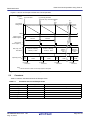
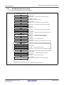
Table 1.1 lists the Peripheral Functions and Their Applications. Figure 1.1 shows the Relationship Between
Date, Day, and Time Data. Figure 1.2 shows the Transition Between Operating Modes.
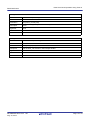
Table 1.1
Peripheral Functions and Their Applications
Peripheral Function
Timer A0 in timer mode
Timer A1
fXCIN (32.768 kHz)
Data for
the number
of seconds
Figure 1.1
1/32
Application
1 second counter
Generates wait time for sub clock oscillation
1 second (1 Hz)
Timer A0 16-bit counter 1/1024
Data for
the number
of minutes
Data for
the number
of hours
Data for
the day of
the week
Data for
the date
Data for
the month
Data for
the year
Relationship Between Date, Day, and Time Data
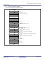
Operating modes
Low power
mode
Wait mode
WAIT
instruction
Figure 1.2
Low power
mode
Timer A0
interrupt
generated
Wait mode
WAIT
instruction
Low power
mode
Timer A0
interrupt
generated
Transition Between Operating Modes
R01AN0859EJ0100 Rev. 1.00
Aug. 24, 2012
Page 3 of 21
Real-Time Clock Operation Using Timer A
R32C/100 Series
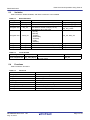
2.
Operation Confirmation Conditions
The sample code accompanying this application note has been run and confirmed under the conditions
below.
Table 2.1
Operation Confirmation Conditions
Item
MCU used
Contents
R5F64189DFD (R32C/118 Group)
When in PLL mode
• Main clock: 16 MHz
• PLL clock: 100 MHz
• Base clock: 50 MHz
• CPU clock: 50 MHz
• Peripheral bus clock: 25 MHz
• Peripheral function clock source: 25 MHz
Operating frequencies
Operating voltage
Integrated development
environment
C compiler
Operating mode
Sample code version
3.
When in low power mode
• Main clock is stopped
• PLL clock is stopped
• Base clock: 32.768 kHz (sub clock: 32.768 kHz)
• CPU clock: 32.768 kHz
• Peripheral bus clock: 16.384 kHz
• Peripheral function clock source is stopped
5V
Renesas Electronics Corporation
High-performance Embedded Workshop Version 4.08
Renesas Electronics Corporation
R32C/100 Series C Compiler V.1.02 Release 01
Compile options
-D__STACKSIZE__=0X300 -D__ISTACKSIZE__=0X300
-DVECTOR_ADR=0x0FFFFFBDC -c -finfo -dir "$(CONFIGDIR)"
(Default setting is used in the integrated development environment.)
Single-chip mode
Version 1.00
Reference Application Notes
Application notes associated with this application note are listed below. Refer to these application notes for
additional information.
• R32C/100 Series Configuring PLL Mode (REJ05B1221-0100)
• R32C/100 Series Entering Low-speed Mode (REJ05B1222-0100)
• R32C/100 Series Configuring Wait Mode (REJ05B1223-0100)
R01AN0859EJ0100 Rev. 1.00
Aug. 24, 2012
Page 4 of 21
Real-Time Clock Operation Using Timer A
R32C/100 Series
4.
Hardware
4.1
Pin Used
Table 4.1 lists the Pin Used and Its Function.
Table 4.1
Pin Used and Its Function
Pin Name
P0_0
5.
I/O
Output
Function
Confirm period for transition to wait mode
Software
5.1
Operation Overview
Enter wait mode after setting the operating mode to low power mode. With timer A0 in timer mode, use a
timer A0 interrupt with a 1 second period to exit wait mode. The date, day, and time data are updated in
the timer A0 interrupt handler. Leap day determination is performed when the month changes. After the
data is updated, a WAIT instruction is used to enter wait mode again.
Settings:
• Timer used: Timer A0
• Mode used: Timer mode
• Timer A0 count source: fC32
• Interrupt used: Timer A0 interrupt
• Gate function: Not used
Formula to calculate a 1 second counter:
1000 ms = (1 ÷ fC32) × (TA0 + 1)
= {1 ÷ (32.768 kHz ÷ 32)} × 1024
= 0.9765625 ms × 1024
(1) Initial setting
Set timer A0 and low power mode as the initial setting.
(2) Timer A0 count start
Set the TA0S bit in the TABSR register to 1 to start the timer A0 count. After the timer A0 count
starts, the real-time clock starts counting from 00:00:00, Saturday, January 1, 2000.
(3) WAIT instruction execution
Execute the WAIT instruction to enter wait mode.
(4) Timer A0 interrupt generation
When timer A0 underflows, the timer A0 interrupt is generated and the MCU exits wait mode.
(5) Timer A0 interrupt handling
Date, day, and time data are updated in the timer A0 interrupt handler. However, the values are
stored in the variable in hexadecimal.
(6) Date, day, and time data initialization
The count continues until 23:59:59, Saturday, December 31, 2099, and then resets to the initial
date and time.
R01AN0859EJ0100 Rev. 1.00
Aug. 24, 2012
Page 5 of 21
Real-Time Clock Operation Using Timer A
R32C/100 Series
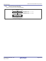
Figure 5.1 shows an Example of Real-Time Clock Operation.
(1) Initial
setting
(2) Count starts
(4) Interrupt generated
(5) Date, day, time data updated
(4)
(5)
(4)
(5)
TA0 register
setting value
0000h
Time
TA0S bit in the 1
TABSR register 0
1 second
1 second
IR bit in the 1
TA0IC register [1]
0
Date, day, and
time data
00:00:00, Saturday,
January 1, 2000
Low
power
mode
Operating mode
(3) WAIT
instruction
00:00:02,
Saturday,
January 1,
2000
00:00:01, Saturday,
January 1, 2000
Low
power
mode
Wait
mode
Wait
mode
(3) WAIT
instruction
Low
power
mode
(3) WAIT
instruction
Wait
mode
23:59:59,
Saturday,
December 31,
2099
Low
power
mode
Wait
mode
(3) WAIT
instruction
Note:
1. This bit becomes 0 when an interrupt request is accepted.
Figure 5.1
5.2
Example of Real-Time Clock Operation
Constants
Table 5.1 lists the Constants Used in the Sample Code.
Table 5.1
Constants Used in the Sample Code
Constant Name
YEAR_MAX
MONTH_MAX
WEEK_MAX
HOUR_MAX
MIN_MAX
SEC_MAX
R01AN0859EJ0100 Rev. 1.00
Aug. 24, 2012
Setting Value
2099
12
6
23
59
59
Contents
Data for the maximum number of years
Data for the maximum number of months
Data for the maximum number of weeks in a month
Data for the maximum number of hours
Data for the maximum number of minutes
Data for the maximum number of seconds
Page 6 of 21
Real-Time Clock Operation Using Timer A
R32C/100 Series
5.3
Variables
Table 5.2 lists the Global Variables, and Table 5.3 lists the const Variable.
Table 5.2
Global Variables
Type
Variable Name
Contents
Function Used
unsigned short
year_cnt
Store data for number of years (2000 to 2099) date_set, leap_day_check
unsigned char
month_cnt Store data for number of months (1 to 12)
date_set, leap_day_check
time_set, date_set,
unsigned char
day_cnt
Store data for number of days (1 to 31)
leap_day_check
Store data for day of the week
0: Sunday
1: Monday
2: Tuesday
time_set, date_set
unsigned char
week_cnt
3: Wednesday
4: Thursday
5: Friday
6: Saturday
unsigned char
hour_cnt
Store data for number of hours (00 to 23)
time_set
unsigned char
min_cnt
Store data for number of minutes (00 to 59)
time_set
unsigned char
sec_cnt
Store data for number of seconds (00 to 59) time_set
Table 5.3
const Variable
Type
Variable Name
const unsigned char day_max_tbl[12]
5.4
Contents
Function Used
Data table for the maximum number of
date_set
days per month
Functions
Table 5.4 lists the Functions.
Table 5.4
Functions
Function Name
timer_a0_int
time_set
date_set
leap_day_check
subclock_set
before_wait_mode_set
power_control
_timer_a0
R01AN0859EJ0100 Rev. 1.00
Aug. 24, 2012
Outline
Timer A0 initial setting
Time setting
Date setting
Leap day determination
Sub clock oscillation setting
Wait mode preset processing
Power control processing
Timer A0 interrupt handling
Page 7 of 21
Real-Time Clock Operation Using Timer A
R32C/100 Series
5.5
Function Specifications
The following tables list the sample code function specifications.
timer_a0_int
Outline
Timer A0 initial setting
Header
None
Declaration
void timer_a0_init(void)
Description
Initial settings to use timer A0 in timer mode.
Argument
None
Returned value
None
Remark
time_set
Outline
Time setting
Header
None
Declaration
Argument
void time_set(void)
After setting the data for the seconds, minutes, hours, date, and day of the week, the
date setting function is called.
None
Returned value
None
Description
Remark
date_set
Outline
Date setting
Header
None
Declaration
Argument
void date_set(void)
The leap day determination function is called, and depending on the result, the date,
month, and year data is set.
None
Returned value
None
Description
Remark
R01AN0859EJ0100 Rev. 1.00
Aug. 24, 2012
Page 8 of 21
Real-Time Clock Operation Using Timer A
R32C/100 Series
leap_day_check
Outline
Leap day determination
Header
None
Declaration
unsigned char leap_day_check(void)
• Leap day is determined.
• Years that can be evenly divided by 4 are determined to have the leap day (February
29). However, years that can be divided by 4 or divided by 100, but cannot be divided
by 400 are determined to not have a leap day.
None
• Leap day: 1
• Not a leap day: 0
Description
Argument
Returned value
Remark
subclock_set
Outline
Sub clock oscillation setting
Header
None
Declaration
Argument
void subclock_set(void)
After setting both bits PD8_6 and PD8_7 in the PD8 register to 0 (input mode) and the
PU25 bit in the PUR2 register to 0 (pull-up resistor unused), set the CM04 bit in the
CM0 register to 1 (XIN-XCIN oscillator).
None
Returned value
None
Remark
Set the oscillation stabilization time according to the manufacturer’s recommendation.
Description
before_wait_mode_set
Outline
Wait mode preset processing
Header
None
Declaration
Argument
void before_wait_mode_set(void)
• Change the base clock source from the PLL clock to the sub clock and enter low
speed mode.
• Stop the main clock and PLL clock, and transition from low speed mode to low power
mode.
None
Returned value
None
Description
Remark
R01AN0859EJ0100 Rev. 1.00
Aug. 24, 2012
Page 9 of 21
Real-Time Clock Operation Using Timer A
R32C/100 Series
power_control
Outline
Power control processing
Header
None
Declaration
Argument
void power_control(void)
Set the interrupt priority level for wake-up, execute the WAIT instruction, and enter wait
mode.
None
Returned value
None
Description
Remark
_timer_a0
Outline
Timer A0 interrupt handling
Header
None
Declaration
void _timer_a0(void)
Description
Call the timer_set function in the interrupt handler.
Argument
None
Returned value
None
Remark
R01AN0859EJ0100 Rev. 1.00
Aug. 24, 2012
Page 10 of 21
Real-Time Clock Operation Using Timer A
R32C/100 Series
5.6
Flowcharts
5.6.1
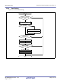
Main Processing
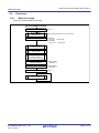
Figure 5.2 shows the Main Processing.
main
Disable maskable interrupts
PLL clock setting
SetPLLClock()
Initialize port P0_0
I flag ← 0
Clock frequencies used in PLL mode are set.
P0 register
P0_0 bit ← 1: Output high
PD0 register
PD0_0 bit ← 1: Output port
Timer A0 initial setting
timer_a0_init()
Sub clock oscillation setting
subclock_set()
Wait mode
preset processing
before_wait_mode_set()
Initialize the fC
divide-by-32 divider
CPSRF register
CPSR bit ← 1
Timer A0 count starts
TABSR register
TA0S bit ← 1
Enable maskable interrupts
I flag ← 1
Power control processing
power_control()
Figure 5.2
Main Processing
R01AN0859EJ0100 Rev. 1.00
Aug. 24, 2012
Page 11 of 21
Real-Time Clock Operation Using Timer A
R32C/100 Series
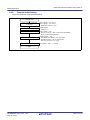
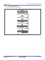
5.6.2
Timer A0 Initial Setting
Figure 5.3 shows the Timer A0 Initial Setting.
timer_a0_init
Set the interrupt priority level
for wake-up
Stop timer A0 count
Disable timer A0 interrupt
Set timer A0 mode register
Set timer A0 register
RIPL1 register ← 07h: Level 7
RIPL2 register ← 07h: Level 7
Bits RLVL2 to RLVL0 = 111b
TABSR register
TA0S bit ← 0
TA0IC register ← 00h
Bits ILVL2 to ILVL0 = 000b: Level 0 (interrupt disabled)
IR bit = 0: No interrupt requested
TA0MR register ← C0h
Bits TMOD1 and TMOD0 = 00b: Timer mode
Bits MR2 and MR1 = 00b: No gate function
Bits TCK1 and TCK0 = 11b: fC32
TA0 register ← 1024 - 1: 1 second
return
Figure 5.3
Timer A0 Initial Setting
R01AN0859EJ0100 Rev. 1.00
Aug. 24, 2012
Page 12 of 21
Real-Time Clock Operation Using Timer A
R32C/100 Series
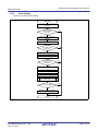
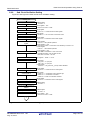
5.6.3
Time Setting
Figure 5.4 shows the Time Setting.
time_set
Update data for number of
seconds
Is number
of seconds more
than 59?
No
Yes
Update data for number of
minutes
Set number of seconds to 00
Is number
of minutes more
than 59?
No
Yes
Update data for number of hours
Set number of minutes to 00
Is number
of hours more
than 23?
No
Yes
Update data for date
Update data for day of the week
Set number of hours to 00
Date setting
date_set()
Has 1 week elapsed?
No
Yes
Set day of the week data to
Sunday
return
Figure 5.4
Time Setting
R01AN0859EJ0100 Rev. 1.00
Aug. 24, 2012
Page 13 of 21
Real-Time Clock Operation Using Timer A
R32C/100 Series
5.6.4
Date Setting
Figure 5.5 shows the Date Setting.
date_set
More than maximum
number of days for this
month?
No
Yes
Leap day determination
leap_day_check()
No
Leap day?
Yes
Update data for month
Set the date to the first
Number of months
is more than 12?
No
Yes
Update data for year
Set month data to January
Number of years
is more than 2099?
No
Yes
Set year data to 2000
Set day of week data to Saturday
return
Figure 5.5
Date Setting
R01AN0859EJ0100 Rev. 1.00
Aug. 24, 2012
Page 14 of 21
Real-Time Clock Operation Using Timer A
R32C/100 Series
5.6.5
Leap Day Determination
Figure 5.6 shows the Leap Day Determination.
leap_day_check
Set 0 to the return value
(not a leap day)
No
Is the date February 29?
Yes
No
Can the year
be divided by 4?
Yes
Set 1 (leap day) to the results
No
Can the year be
divided by 100?
Yes
Set 0 (not a leap day) to the results
Can the year be
divided by 400?
No
Yes
Set 1 (leap day) to the results
return
Figure 5.6
Leap Day Determination
R01AN0859EJ0100 Rev. 1.00
Aug. 24, 2012
Page 15 of 21
Real-Time Clock Operation Using Timer A
R32C/100 Series
5.6.6
Sub Clock Oscillation Setting
Figure 5.7 and Figure 5.8 show the sub clock oscillation setting.
subclock_set
Stop timer A1 count
TABSR register
TA1S bit ← 0
Disable timer A1 interrupt
TA1IC register ← 00h
Bits ILVL2 to ILVL0 = 000b
Enable writing to register
PRCR register
PRC1 bit ← 1: Enable to write to PM2 register
Set processor mode register 2
Disable writing to register
Set count source prescaler
register
Set timer A1 mode register
Set timer A1 register
Set XCIN-XCOUT pins
Enable writing to register
Set system clock
control register 0
Disable writing to register
Start timer A1 count
PM2 register
PM26 bit ← 1: f2n clock source is the main clock
PRCR register
PRC1 bit ← 0: Disable to write to PM2 register
TCSPR register
CST bit ← 0: Stop divider operation
TCSPR register ← 0Ah
Bits CNT3 to CNT0 = 1010b: Main clock divided by 2n where n=10
TCSPR register
CST bit ← 1: Start divider operation
TA1MR register ← 80h
Bits TMOD1 and TMOD0 = 00b: Timer mode
Bits MR2 and MR1 = 00b: No gate function
Bits TCK1 and TCK0 = 10b: f2n
TA1 register ← 40000 - 1: 50 ms
PD8 register
PD8_6 bit ← 0: Input port
PD8_7 bit ← 0: Input port
PUR2 register
PU25 bit ← 0: P8_6 and P8_7 pull-up resistor disabled
PRCR register
PRC0 bit ← 1: Enable to write to CM0 register
CM0 register
CM03 bit ← 1: XCIN-XCOUT drive strength high
CM04 bit ← 1: XCIN-XCOUT oscillator
CM05 bit ← 0: Main clock oscillator enabled
PRCR register
PRC0 bit ← 0: Disable to write to CM0 register
TABSR register
TA1S bit ← 1
Wait for sub clock oscillator to
stabilize
Stop timer A1 count
Disable timer A1 interrupt
TABSR register
TA1S bit ← 0
TA1IC register ← 00h
Bits ILVL2 to ILVL0 = 000b
A
Figure 5.7
Sub Clock Oscillation Setting (1/2)
R01AN0859EJ0100 Rev. 1.00
Aug. 24, 2012
Page 16 of 21
Real-Time Clock Operation Using Timer A
R32C/100 Series
A
Set count source prescaler
register
Enable writing to register
Set processor mode register 2
Disable writing to register
TCSPR register
CST bit ← 0: Stop divider operation
PRCR register
PRC1 bit ← 1: Enable to write to PM2 register
PM2 register
PM26 bit ← 0: f2n clock source is peripheral clock source
PRCR register
PRC1 bit ← 0: Disable to write to PM2 register
return
Figure 5.8
Sub Clock Oscillation Setting (2/2)
R01AN0859EJ0100 Rev. 1.00
Aug. 24, 2012
Page 17 of 21
Real-Time Clock Operation Using Timer A
R32C/100 Series
5.6.7
Wait Mode Preset Processing
Figure 5.9 shows Wait Mode Preset Processing.
before_wait_mode_set
Enable writing to register
Set low speed mode base clock
PRCR2 register
PRC27 bit ← 1: Enable to write to the CM3 register
CM3 register ← 00h
Bits CM31 and CM30 = 00b: fC
Disable writing to register
PRCR2 register
PRC27 bit ← 0: Disable to write to the CM3 register
Enable writing to register
PRR register ← AAh: Enable to write to the CCR register
Set base clock source
CCR register
BCS bit ← 1: fC
Disable writing to register
PRR register ← 00h: Disable to write to the CCR register
Enable writing to registers
PRCR register
PRC0 bit ← 1: Enable to write to registers CM0 and CM1
Set system clock
control register 0
Stop PLL oscillator
Disable writing to registers
CM0 register
CM03 bit ← 0: XCIN-XCOUT drive strength low
CM05 bit ← 1: Main clock oscillator disabled
CM1 register
CM10 bit ← 1: PLL oscillator disabled
PRCR register
PRC0 bit ← 0: Disable to write to registers CM0 and CM1
(See Note 1)
Enable writing to register
Set CPU rewrite mode
PRR register ← AAh: Enable to write to the FMCR register
FMCR register
FEW bit ← 0: Normal operating mode
Disable writing to register
PRR register ← 00h: Disable to write to the FMCR register
Enable writing to register
PRCR3 register
PRC31 bit ← 1: Enable to write to VRCR register
Main regulator shut-down
VRCR register
MRS bit ← 1: Main regulator stopped
Disable writing to register
PRCR3 register
PRC31 bit ← 0: Disable to write to VRCR register
return
Note:
1. Perform this processing when using an embedded CPU rewrite program.
Figure 5.9
Wait Mode Preset Processing
R01AN0859EJ0100 Rev. 1.00
Aug. 24, 2012
Page 18 of 21
Real-Time Clock Operation Using Timer A
R32C/100 Series
5.6.8
Power Control Processing
Figure 5.10 shows the Power Control Processing.
power_control
Disable maskable interrupts
Disable the timer A0 interrupt
I flag ← 0
TA0IC register ← 00h
Bits ILVL2 to ILVL0 = 000b
Perform a dummy read
Set the processor interrupt
priority level to 0
Enable maskable interrupts
I flag ← 1
Insert two NOP instructions
Disable maskable interrupts
Enable timer A0 interrupt
I flag ← 0
TA0IC register ← 07h
Bits ILVL2 to ILVL0 = 111b: Level 7
Set the processor interrupt
priority level to 3
Set the wake-up IPL setting
registers
Enable writing to register
Set system clock
control register 0
Disable writing to register
RIPL1 register ← 03h
Bits RLVL2 to RLVL0 = 011b: Level 3
RIPL2 register ← 03h
Bits RLVL2 to RLVL0 = 011b: Level 3
PRCR register
PRC0 bit ← 1: Enable to write to CM0 register
CM0 register
CM02 bit ← 1: Peripheral clock source stopped in wait mode
PRCR register
PRC0 bit ← 0: Disable to write to CM0 register
Enable maskable interrupts
I flag ← 1
Set port P0_0 to output low
P0 register
P0_0 bit ← 0
Execute WAIT instruction
Set port P0_0 to output high
P0 register
P0_0 bit ← 1
return
Figure 5.10
Power Control Processing
R01AN0859EJ0100 Rev. 1.00
Aug. 24, 2012
Page 19 of 21
Real-Time Clock Operation Using Timer A
R32C/100 Series
5.6.9
Timer A0 Interrupt Handling
Figure 5.11 shows the Timer A0 Interrupt Handling.
_timer_a0
Set the interrupt priority level for
wake-up
RIPL1 register ← 07h
Bits RLVL2 to RLVL0 = 111b: Level 7
RIPL2 register ← 07h
Bits RLVL2 to RLVL0 = 111b: Level 7
Time setting
time_set()
return
Figure 5.11
Timer A0 Interrupt Handling
R01AN0859EJ0100 Rev. 1.00
Aug. 24, 2012
Page 20 of 21
R32C/100 Series
6.
Real-Time Clock Operation Using Timer A
Sample Code
Sample code can be downloaded from the Renesas Electronics website.
7.
Reference Documents
R32C/116 Group User’s Manual: Hardware Rev.1.10
R32C/117 Group User’s Manual: Hardware Rev.1.10
R32C/118 Group User’s Manual: Hardware Rev.1.10
The latest versions can be downloaded from the Renesas Electronics website.
Technical Update/Technical News
The latest information can be downloaded from the Renesas Electronics website.
C Compiler Manual
R32C/100 Series C Compiler Package V.1.02
C Compiler User’s Manual Rev.2.00
The latest version can be downloaded from the Renesas Electronics website.
Website and Support
Renesas Electronics website
http://www.renesas.com/
Inquiries
http://www.renesas.com/contact/
R01AN0859EJ0100 Rev. 1.00
Aug. 24, 2012
Page 21 of 21
R32C/100 Series
Real-Time Clock Operation Using Timer A
Revision History
Rev.
Date
1.00
Aug. 24, 2012
Description
Page
—
Summary
First edition issued
All trademarks and registered trademarks are the property of their respective owners.
A-1
General Precautions in the Handling of MPU/MCU Products
The following usage notes are applicable to all MPU/MCU products from Renesas. For detailed usage notes
on the products covered by this manual, refer to the relevant sections of the manual. If the descriptions under
General Precautions in the Handling of MPU/MCU Products and in the body of the manual differ from each
other, the description in the body of the manual takes precedence.
1. Handling of Unused Pins
Handle unused pins in accord with the directions given under Handling of Unused Pins in the
manual.
The input pins of CMOS products are generally in the high-impedance state. In operation
with an unused pin in the open-circuit state, extra electromagnetic noise is induced in the
vicinity of LSI, an associated shoot-through current flows internally, and malfunctions occur
due to the false recognition of the pin state as an input signal become possible. Unused
pins should be handled as described under Handling of Unused Pins in the manual.
2. Processing at Power-on
The state of the product is undefined at the moment when power is supplied.
The states of internal circuits in the LSI are indeterminate and the states of register
settings and pins are undefined at the moment when power is supplied.
In a finished product where the reset signal is applied to the external reset pin, the states
of pins are not guaranteed from the moment when power is supplied until the reset
process is completed.
In a similar way, the states of pins in a product that is reset by an on-chip power-on reset
function are not guaranteed from the moment when power is supplied until the power
reaches the level at which resetting has been specified.
3. Prohibition of Access to Reserved Addresses
Access to reserved addresses is prohibited.
The reserved addresses are provided for the possible future expansion of functions. Do
not access these addresses; the correct operation of LSI is not guaranteed if they are
accessed.
4. Clock Signals
After applying a reset, only release the reset line after the operating clock signal has become
stable. When switching the clock signal during program execution, wait until the target clock
signal has stabilized.
When the clock signal is generated with an external resonator (or from an external
oscillator) during a reset, ensure that the reset line is only released after full stabilization of
the clock signal. Moreover, when switching to a clock signal produced with an external
resonator (or by an external oscillator) while program execution is in progress, wait until
the target clock signal is stable.
5. Differences between Products
Before changing from one product to another, i.e. to one with a different part number, confirm
that the change will not lead to problems.
The characteristics of MPU/MCU in the same group but having different part numbers may
differ because of the differences in internal memory capacity and layout pattern. When
changing to products of different part numbers, implement a system-evaluation test for
each of the products.
Notice
1.
Descriptions of circuits, software and other related information in this document are provided only to illustrate the operation of semiconductor products and application examples. You are fully responsible for
the incorporation of these circuits, software, and information in the design of your equipment. Renesas Electronics assumes no responsibility for any losses incurred by you or third parties arising from the
use of these circuits, software, or information.
2.
Renesas Electronics has used reasonable care in preparing the information included in this document, but Renesas Electronics does not warrant that such information is error free. Renesas Electronics
3.
Renesas Electronics does not assume any liability for infringement of patents, copyrights, or other intellectual property rights of third parties by or arising from the use of Renesas Electronics products or
assumes no liability whatsoever for any damages incurred by you resulting from errors in or omissions from the information included herein.
technical information described in this document. No license, express, implied or otherwise, is granted hereby under any patents, copyrights or other intellectual property rights of Renesas Electronics or
others.
4.
You should not alter, modify, copy, or otherwise misappropriate any Renesas Electronics product, whether in whole or in part. Renesas Electronics assumes no responsibility for any losses incurred by you or
5.
Renesas Electronics products are classified according to the following two quality grades: "Standard" and "High Quality". The recommended applications for each Renesas Electronics product depends on
third parties arising from such alteration, modification, copy or otherwise misappropriation of Renesas Electronics product.
the product's quality grade, as indicated below.
"Standard": Computers; office equipment; communications equipment; test and measurement equipment; audio and visual equipment; home electronic appliances; machine tools; personal electronic
equipment; and industrial robots etc.
"High Quality": Transportation equipment (automobiles, trains, ships, etc.); traffic control systems; anti-disaster systems; anti-crime systems; and safety equipment etc.
Renesas Electronics products are neither intended nor authorized for use in products or systems that may pose a direct threat to human life or bodily injury (artificial life support devices or systems, surgical
implantations etc.), or may cause serious property damages (nuclear reactor control systems, military equipment etc.). You must check the quality grade of each Renesas Electronics product before using it
in a particular application. You may not use any Renesas Electronics product for any application for which it is not intended. Renesas Electronics shall not be in any way liable for any damages or losses
incurred by you or third parties arising from the use of any Renesas Electronics product for which the product is not intended by Renesas Electronics.
6.
You should use the Renesas Electronics products described in this document within the range specified by Renesas Electronics, especially with respect to the maximum rating, operating supply voltage
range, movement power voltage range, heat radiation characteristics, installation and other product characteristics. Renesas Electronics shall have no liability for malfunctions or damages arising out of the
use of Renesas Electronics products beyond such specified ranges.
7.
Although Renesas Electronics endeavors to improve the quality and reliability of its products, semiconductor products have specific characteristics such as the occurrence of failure at a certain rate and
malfunctions under certain use conditions. Further, Renesas Electronics products are not subject to radiation resistance design. Please be sure to implement safety measures to guard them against the
possibility of physical injury, and injury or damage caused by fire in the event of the failure of a Renesas Electronics product, such as safety design for hardware and software including but not limited to
redundancy, fire control and malfunction prevention, appropriate treatment for aging degradation or any other appropriate measures. Because the evaluation of microcomputer software alone is very difficult,
please evaluate the safety of the final products or systems manufactured by you.
8.
Please contact a Renesas Electronics sales office for details as to environmental matters such as the environmental compatibility of each Renesas Electronics product. Please use Renesas Electronics
products in compliance with all applicable laws and regulations that regulate the inclusion or use of controlled substances, including without limitation, the EU RoHS Directive. Renesas Electronics assumes
no liability for damages or losses occurring as a result of your noncompliance with applicable laws and regulations.
9.
Renesas Electronics products and technology may not be used for or incorporated into any products or systems whose manufacture, use, or sale is prohibited under any applicable domestic or foreign laws or
regulations. You should not use Renesas Electronics products or technology described in this document for any purpose relating to military applications or use by the military, including but not limited to the
development of weapons of mass destruction. When exporting the Renesas Electronics products or technology described in this document, you should comply with the applicable export control laws and
regulations and follow the procedures required by such laws and regulations.
10. It is the responsibility of the buyer or distributor of Renesas Electronics products, who distributes, disposes of, or otherwise places the product with a third party, to notify such third party in advance of the
contents and conditions set forth in this document, Renesas Electronics assumes no responsibility for any losses incurred by you or third parties as a result of unauthorized use of Renesas Electronics
products.
11. This document may not be reproduced or duplicated in any form, in whole or in part, without prior written consent of Renesas Electronics.
12. Please contact a Renesas Electronics sales office if you have any questions regarding the information contained in this document or Renesas Electronics products, or if you have any other inquiries.
(Note 1)
"Renesas Electronics" as used in this document means Renesas Electronics Corporation and also includes its majority-owned subsidiaries.
(Note 2)
"Renesas Electronics product(s)" means any product developed or manufactured by or for Renesas Electronics.
http://www.renesas.com
SALES OFFICES
Refer to "http://www.renesas.com/" for the latest and detailed information.
Renesas Electronics America Inc.
2880 Scott Boulevard Santa Clara, CA 95050-2554, U.S.A.
Tel: +1-408-588-6000, Fax: +1-408-588-6130
Renesas Electronics Canada Limited
1101 Nicholson Road, Newmarket, Ontario L3Y 9C3, Canada
Tel: +1-905-898-5441, Fax: +1-905-898-3220
Renesas Electronics Europe Limited
Dukes Meadow, Millboard Road, Bourne End, Buckinghamshire, SL8 5FH, U.K
Tel: +44-1628-651-700, Fax: +44-1628-651-804
Renesas Electronics Europe GmbH
Arcadiastrasse 10, 40472 Düsseldorf, Germany
Tel: +49-211-65030, Fax: +49-211-6503-1327
Renesas Electronics (China) Co., Ltd.
7th Floor, Quantum Plaza, No.27 ZhiChunLu Haidian District, Beijing 100083, P.R.China
Tel: +86-10-8235-1155, Fax: +86-10-8235-7679
Renesas Electronics (Shanghai) Co., Ltd.
Unit 204, 205, AZIA Center, No.1233 Lujiazui Ring Rd., Pudong District, Shanghai 200120, China
Tel: +86-21-5877-1818, Fax: +86-21-6887-7858 / -7898
Renesas Electronics Hong Kong Limited
Unit 1601-1613, 16/F., Tower 2, Grand Century Place, 193 Prince Edward Road West, Mongkok, Kowloon, Hong Kong
Tel: +852-2886-9318, Fax: +852 2886-9022/9044
Renesas Electronics Taiwan Co., Ltd.
13F, No. 363, Fu Shing North Road, Taipei, Taiwan
Tel: +886-2-8175-9600, Fax: +886 2-8175-9670
Renesas Electronics Singapore Pte. Ltd.
80 Bendemeer Road, Unit #06-02 Hyflux Innovation Centre Singapore 339949
Tel: +65-6213-0200, Fax: +65-6213-0300
Renesas Electronics Malaysia Sdn.Bhd.
Unit 906, Block B, Menara Amcorp, Amcorp Trade Centre, No. 18, Jln Persiaran Barat, 46050 Petaling Jaya, Selangor Darul Ehsan, Malaysia
Tel: +60-3-7955-9390, Fax: +60-3-7955-9510
Renesas Electronics Korea Co., Ltd.
11F., Samik Lavied' or Bldg., 720-2 Yeoksam-Dong, Kangnam-Ku, Seoul 135-080, Korea
Tel: +82-2-558-3737, Fax: +82-2-558-5141
© 2012 Renesas Electronics Corporation. All rights reserved.
Colophon 2.2