1
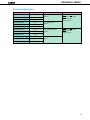
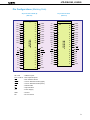
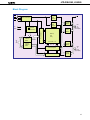
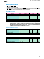
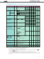
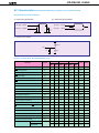
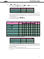
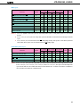
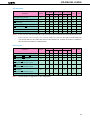
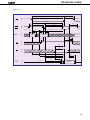
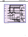
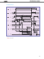
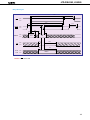
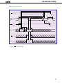
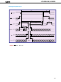
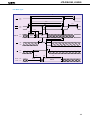
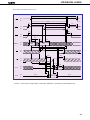
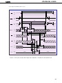
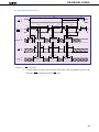
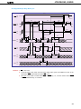
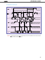
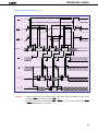
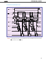
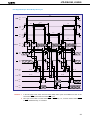
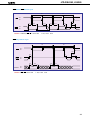
DATA SHEET
MOS INTEGRATED CIRCUIT
µPD42S4260, 424260
4 M-BIT DYNAMIC RAM
256 K-WORD BY 16-BIT, FAST PAGE MODE, BYTE READ/WRITE MODE
Description
The µ PD42S4260, 424260 are 262,144 words by 16 bits dynamic CMOS RAMs. The fast page mode and byte
read/write mode capability realize high speed access and low power consumption.
Besides, the µPD42S4260 can execute CAS before RAS self refresh.
These are packaged in 44-pin plastic TSOP (II) and 40-pin plastic SOJ.
Features
• 262,144 words by 16 bits organization
• Single +5.0 V ±10 % power supply
• Fast access and cycle time
Power consumption
Active (MAX.)
Part number
Access time
(MAX.)
R/W cycle time
(MIN.)
Fast page mode
cycle time (MIN.)
µPD42S4260-60, 424260-60
880.0 mW
60 ns
110 ns
40 ns
µPD42S4260-70, 424260-70
880.0 mW
70 ns
130 ns
45 ns
µPD42S4260-80, 424260-80
797.5 mW
80 ns
150 ns
50 ns
• The µPD42S4260 can execute CAS before RAS self refresh
Refresh
Power consumption at standby
(MAX.)
Part number
Refresh cycle
µPD42S4260
512 cycles / 128 ms
CAS before RAS self refresh,
CAS before RAS refresh,
RAS only refresh, Hidden refresh
0.825 mW
(CMOS level input)
µPD424260
512 cycles / 8 ms
CAS before RAS refresh,
RAS only refresh,
Hidden refresh
5.5 mW
(CMOS level input)
• Multiplexed address inputs ... Row address: A0 to A8, Column address: A0 to A8
The information in this document is subject to change without notice.
Document No. M11089EJ5V0DSU1
1
©
1995
µ PD42S4260, 424260
Ordering Information
Part number
Access time (MAX.)
µPD42S4260G5-60
60 ns
µPD42S4260G5-70
70 ns
µPD42S4260G5-80
80 ns
µPD42S4260LE-60
60 ns
µPD42S4260LE-70
70 ns
µPD42S4260LE-80
80 ns
µPD424260G5-60
60 ns
µPD424260G5-70
70 ns
µPD424260G5-80
80 ns
µPD424260LE-60
60 ns
µPD424260LE-70
70 ns
µPD424260LE-80
80 ns
Package
44-pin Plastic TSOP (II)
(400 mil)
Refresh
CAS before RAS self refresh
CAS before RAS refresh
RAS only refresh
Hidden refresh
40-pin Plastic SOJ
(400 mil)
44-pin Plastic TSOP (II)
(400 mil)
CAS before RAS refresh
RAS only refresh
Hidden refresh
40-pin Plastic SOJ
(400 mil)
2
µ PD42S4260, 424260
Pin Configurations (Marking Side)
44-pin Plastic TSOP (II)
40-pin Plastic SOJ
(400 mil)
(400 mil)
44
GND
VCC
1
40
GND
2
43
I/O16
I/O1
2
39
I/O16
I/O2
3
42
I/O15
I/O2
3
38
I/O15
I/O3
4
41
I/O14
I/O3
4
37
I/O14
I/O4
5
40
I/O13
I/O4
5
36
I/O13
VCC
6
39
GND
VCC
6
35
GND
I/O5
7
38
I/O12
I/O5
7
34
I/O12
I/O6
8
37
I/O11
I/O6
8
33
I/O11
I/O7
9
36
I/O10
I/O7
9
32
I/O10
I/O8
10
35
I/O9
I/O8
10
NC
11
NC
13
32
NC
NC
14
31
LCAS
WE
15
30
UCAS
RAS
16
29
OE
NC
17
28
A8
A0
18
27
A7
A1
19
26
A6
A2
20
25
A5
A3
21
24
A4
VCC
22
23
GND
A0 to A8
µ PD42S4260LE
µ PD424260LE
1
µ PD42S4260G5
µ PD424260G5
VCC
I/O1
31
I/O9
30
NC
29
LCAS
28
UCAS
NC
12
WE
13
RAS
14
27
OE
NC
15
26
A8
A0
16
25
A7
A1
17
24
A6
A2
18
23
A5
A3
19
22
A4
VCC
20
21
GND
: Address Inputs
I/O1 to I/O16 : Data Inputs/Outputs
RAS
: Row Address Strobe
UCAS
: Column Address Strobe (upper)
LCAS
: Column Address Strobe (lower)
WE
: Write Enable
OE
: Output Enable
V CC
: Power Supply
GND
: Ground
NC
: No Connection
3
µ PD42S4260, 424260
Block Diagram
RAS
LCAS
UCAS
WE
Lower
Byte
Control
Clock Generator
OE
Data
Output
Buffer
Upper
Byte
Control
VCC
A0
to
A8
CAS before
RAS Counter
Row
Address
Buffer
Column
Address
Buffer
X0 to X8
512
Data
Input
Buffer
Row Decoder
GND
I/O1
to
I/O8
(Lower Byte)
Memory
Cell
Array
512 × 512 × 16
Data
Output
Buffer
512 × 16
Y0 to Y8
Sense Amplifier
512
Column Decoder
I/O9
to
I/O16
(Upper Byte)
× 16
Data
Input
Buffer
4
µ PD42S4260, 424260
Input/Output Pin Functions
The µ PD42S4260, 424260 have input pins RAS, CAS Note, WE, OE, A0 to A8 and input/output pins I/O1 to
I/O16.
Pin name
Input/
Output
Function
RAS
(Row address
strobe)
Input
RAS activates the sense amplifier by latching a row address (A0 to A8) and selecting a
corresponding word line.
It refreshes memory cell array of one line selected by the row address (A0 to A8).
It also selects the following function.
• CAS before RAS refresh
CAS
(Column address
strobe)
Input
CAS activates data input/output circuit by latching column address (A0 to A8) and selecting a digit line connected with the sense amplifier.
A0 to A8
(Address input)
Input
9-bit address bus.
Input total 18-bit of address signal, upper 9-bit and lower 9-bit in sequence (address
multiplex method).
Therefore, one word (16-bit) is selected from 262,144-word by 16-bit memory cell array.
In actual operation, latch row address by specifying row address and activating RAS.
Then, switch the address bus to column address and activate CAS.
Each address is taken into the device when RAS and CAS are activated.
Therefore, the address input setup time (tASR, t ASC) and hold time (tRAH , tCAH ) are specified
for the activation of RAS and CAS.
WE
(Write enable)
Input
Write control signal.
Write operation is executed by activating RAS, CAS and WE.
OE
(Output enable)
Input
Read control signal.
Read operation can be executed by activating RAS, CAS and OE.
If WE is activated during read operation, OE is to be ineffective in the device.
Therefore, read operation cannot be executed.
I/O1 to I/O16
(Data input/
output)
Input/
Output
16-bit data bus.
I/O1 to I/O16 are used to input/output data.
Note CAS means UCAS and LCAS.
5
µ PD42S4260, 424260
Electrical Specifications
• CAS means UCAS and LCAS.
• All voltages are referenced to GND.
• After power up (VCC ≥ VCC (MIN.)), wait more than 100 µ s (RAS, CAS inactive) and then, execute eight CAS before
RAS or RAS only refresh cycles as dummy cycles to initialize internal circuit.
Absolute Maximum Ratings
Parameter
Symbol
Condition
Rating
Unit
Voltage on any pin relative to GND
VT
–1.0 to +7.0
V
Supply voltage
VCC
–1.0 to +7.0
V
Output current
IO
50
mA
Power dissipation
PD
1
W
Operating ambient temperature
TA
0 to +70
˚C
Storage temperature
Tstg
–55 to +125
˚C
Caution
Exposing the device to stress above those listed in Absolute Maximum Ratings could cause
permanent damage. The device is not meant to be operated under conditions outside the limits
described in the operational section of this specification. Exposure to Absolute Maximum Rating
conditions for extended periods may affect device reliability.
Recommended Operating Conditions
Parameter
Symbol
Condition
MIN.
TYP.
MAX.
Unit
5.0
5.5
V
Supply voltage
VCC
4.5
High level input voltage
VIH
2.4
VCC +1.0
V
Low level input voltage
VIL
–1.0
+0.8
V
Operating ambient temperature
TA
0
70
˚C
MAX.
Unit
Capacitance (TA = 25 ˚C, f = 1 MHz)
Parameter
Input capacitance
Data input/output capacitance
Symbol
Test condition
MIN.
TYP.
CI1
Address
5
pF
CI2
RAS, CAS, WE, OE
7
pF
CI /O
I/O
7
pF
6
µ PD42S4260, 424260
DC Characteristics
Parameter
Operating current
Standby
current
µ PD42S4260
(Recommended Operating Conditions unless otherwise noted)
Symbol
I CC1
I CC2
Test condition
RAS, CAS cycling
t RC = tRC (MIN.) , IO = 0 mA
MIN.
MAX.
Unit
Notes
t RAC = 60 ns
160
mA
1, 2, 3
t RAC = 70 ns
160
t RAC = 80 ns
145
RAS, CAS ≥ V IH (MIN.), I O = 0 mA
2
RAS, CAS ≥ V CC – 0.2 V, I O = 0 mA
µPD424260
RAS only refresh current
Operating current
(Fast page mode)
CAS before RAS
refresh current
CAS before RAS
I CC3
I CC4
I CC5
I CC6
long refresh current
(512 cycles / 128 ms,
only for the µ PD42S4260)
TYP.
0.15
RAS, CAS ≥ V IH (MIN.), I O = 0 mA
2
RAS, CAS ≥ V CC – 0.2 V, I O = 0 mA
1
RAS cycling, CAS ≥ VIH (MIN.)
t RC = tRC (MIN.) , IO = 0 mA
t RAC = 60 ns
160
t RAC = 70 ns
160
t RAC = 80 ns
145
t RAC = 60 ns
140
t RAC = 70 ns
140
t RAC = 80 ns
130
t RAC = 60 ns
160
t RAC = 70 ns
160
t RAC = 80 ns
145
CAS before RAS refresh:
t RC = 250.0 µs
RAS, CAS:
VCC – 0.2 V ≤ V IH ≤ V IH(MAX.)
0V ≤ V IL ≤ 0.2 V
t RAS ≤ 200 ns
Standby:
RAS, CAS ≥ V CC – 0.2 V
Address: VIH or VIL
WE, OE: VIH
I O = 0 mA
t RAS ≤ 1 µs
RAS ≤ VIL (MAX.), CAS cycling
t PC = tPC (MIN.), IO = 0 mA
RAS cycling
t RC = tRC (MIN.) , IO = 0 mA
mA
mA
1, 2, 3, 4
mA
1, 2, 5
mA
1, 2
200
µA
1, 2
300
µA
1, 2
150
µA
2
Self refresh current
(CAS before RAS self
refresh, only for the
µPD42S4260)
I CC7
RAS, CAS:
tRASS = 5 ms
VCC – 0.2 V ≤ VIH ≤ VIH (MAX.)
0 V ≤ VIL ≤ 0.2 V
I O = 0 mA
Input leakage current
I I(L)
VI = 0 to 5.5 V
All other pins not under test = 0 V
–10
+10
µA
Output leakage current
I O(L)
VO = 0 to 5.5 V
Output is disabled (Hi-Z)
–10
+10
µA
High level output voltage
VOH
I O = –2.5 mA
2.4
Low level output voltage
VOL
I O = +2.1 mA
V
0.4
V
Notes 1. ICC1 , ICC3 , ICC4 , ICC5 and ICC6 depend on cycle rates (tRC and tPC).
2. Specified values are obtained with outputs unloaded.
3. ICC1 and ICC3 are measured assuming that address can be changed once or less during RAS ≤
VIL (MAX.) and CAS ≥ V IH (MIN.).
4. ICC3 is measured assuming that all column address inputs are held at either high or low.
5. ICC4 is measured assuming that all column address inputs are switched only once during each fast page
cycle.
7
µ PD42S4260, 424260
AC Characteristics
(Recommended Operating Conditions unless otherwise noted)
AC Characteristics Test Conditions
(1) Input timing specification
VIH
(2) Output timing specification
= 2.4 V
VOH (MIN.) = 2.4 V
VIL (MAX.) = 0.8 V
VOL (MAX.) = 0.4 V
(MIN.)
tT = 5 ns
tT = 5 ns
(3) Output load condition
VCC
1,660 Ω
I/O
100 pF
590 Ω
CL
Common to Read, Write, Read Modify Write Cycle
Parameter
Symbol
t RAC = 60 ns
t RAC = 70 ns
t RAC = 80 ns
MIN.
MAX.
MIN.
MAX.
MIN.
MAX.
Unit
Notes
Read/Write cycle time
t RC
110
–
130
–
150
–
ns
RAS precharge time
tRP
40
–
50
–
60
–
ns
CAS precharge time
t CPN
10
–
10
–
10
–
ns
RAS pulse width
t RAS
60
10,000
70
10,000
80
10,000
ns
CAS pulse width
t CAS
15
10,000
20
10,000
20
10,000
ns
RAS hold time
t RSH
15
–
20
–
20
–
ns
CAS hold time
t CSH
60
–
70
–
80
–
ns
RAS to CAS delay time
tRCD
20
45
20
50
20
60
ns
2
RAS to column address delay time
tRAD
15
30
15
35
15
40
ns
2
CAS to RAS precharge time
t CRP
10
–
10
–
10
–
ns
3
Row address setup time
t ASR
0
–
0
–
0
–
ns
Row address hold time
t RAH
10
–
10
–
10
–
ns
Column address setup time
t ASC
0
–
0
–
0
–
ns
Column address hold time
t CAH
15
–
15
–
15
–
ns
OE lead time referenced to RAS
t OES
0
–
0
–
0
–
ns
CAS to data setup time
t CLZ
0
–
0
–
0
–
ns
OE to data setup time
tOLZ
0
–
0
–
0
–
ns
OE to data delay time
tOED
15
–
15
–
20
–
ns
Masked byte write hold time referenced to RAS
t MRH
0
–
0
–
0
–
ns
tT
3
50
3
50
3
50
ns
t REF
–
128
–
128
–
128
ms
–
8
–
8
–
8
ms
Transition time (rise and fall)
Refresh time
µPD42S4260
µPD424260
1
4
8
µ PD42S4260, 424260
Notes 1. In CAS before RAS refresh cycles, tRAS (MAX.) is 100 µ s.
If 10 µ s < tRAS < 100 µs, RAS precharge time for CAS before RAS self refresh (tRPS) is applied.
2. For read cycles, access time is defined as follows:
Input conditions
Access time
Access time from RAS
t RAD ≤ t RAD (MAX.) and t RCD ≤ tRCD (MAX.)
t RAC (MAX.)
t RAC (MAX.)
t RAD >t RAD (MAX.) and tRCD ≤ tRCD (MAX.)
t AA (MAX.)
t RAD + tAA (MAX.)
t RCD > tRCD (MAX.)
t CAC (MAX.)
t RCD + tCAC (MAX.)
tRAD (MAX.) and tRCD (MAX.) are specified as reference points only; they are not restrictive operating parameters.
They are used to determine which access time (tRAC, tAA or tCAC) is to be used for finding out when output
data will be available. Therefore, the input conditions tRAD ≥ tRAD (MAX.) and tRCD ≥ tRCD (MAX.) will not cause
any operation problems.
3. tCRP (MIN.) requirement is applied to RAS, CAS cycles.
4. This specification is applied only to the µPD42S4260.
Read Cycle
Parameter
Symbol
t RAC = 60 ns
t RAC = 70 ns
t RAC = 80 ns
MIN.
MAX.
MIN.
MAX.
MIN.
MAX.
Unit
Notes
Access time from RAS
t RAC
–
60
–
70
–
80
ns
1
Access time from CAS
t CAC
–
15
–
20
–
20
ns
1
Access time from column address
tAA
–
30
–
35
–
40
ns
1
Access time from OE
t OEA
–
15
–
20
–
20
ns
Column address lead time referenced to RAS
tRAL
30
–
35
–
40
–
ns
Read command setup time
t RCS
0
–
0
–
0
–
ns
Read command hold time referenced to RAS
tRRH
0
–
0
–
0
–
ns
2
Read command hold time referenced to CAS
tRCH
0
–
0
–
0
–
ns
2
Output buffer turn-off delay time from OE
tOEZ
0
15
0
15
0
20
ns
3
Output buffer turn-off delay time from CAS
tOFF
0
15
0
15
0
20
ns
3
Notes 1. For read cycles, access time is defined as follows:
Input conditions
Access time
Access time from RAS
t RAD ≤ t RAD (MAX.) and t RCD ≤ tRCD (MAX.)
t RAC (MAX.)
t RAC (MAX.)
t RAD >t RAD (MAX.) and tRCD ≤ tRCD (MAX.)
t AA (MAX.)
t RAD + tAA (MAX.)
t RCD > tRCD (MAX.)
t CAC (MAX.)
t RCD + tCAC (MAX.)
tRAD (MAX.) and tRCD (MAX.) are specified as reference points only; they are not restrictive operating parameters.
They are used to determine which access time (tRAC, tAA or tCAC) is to be used for finding out when output
data will be available. Therefore, the input conditions tRAD ≥ tRAD (MAX.) and tRCD ≥ tRCD (MAX.) will not cause
any operation problems.
2. Either tRCH (MIN.) or tRRH (MIN.) should be met in read cycles.
3. tOFF (MAX.) and tOEZ (MAX.) define the time when the output achieves the condition of Hi-Z and is not referenced
to VOH or VOL.
9
µ PD42S4260, 424260
Write Cycle
Parameter
t RAC = 60 ns
t RAC = 70 ns
t RAC = 80 ns
MIN.
MAX.
MIN.
MAX.
MIN.
MAX.
Symbol
Unit
Notes
WE hold time referenced to CAS
tWCH
15
–
15
–
15
–
ns
1
WE pulse width
t WP
10
–
15
–
15
–
ns
1
WE lead time referenced to RAS
t RWL
15
–
20
–
20
–
ns
WE lead time referenced to CAS
t CWL
15
–
15
–
20
–
ns
WE setup time
tWCS
0
–
0
–
0
–
ns
OE hold time
tOEH
0
–
0
–
0
–
ns
Data-in setup time
tDS
0
–
0
–
0
–
ns
3
Data-in hold time
t DH
15
–
15
–
20
–
ns
3
2
Notes 1. tWP (MIN.) is applied to late write cycles or read modify write cycles. In early write cycles, tWCH (MIN.) should
be met.
2. If tWCS ≥ t WCS (MIN.), the cycle is an early write cycle and the data out will remain Hi-Z through the entire
cycle.
3. tDS (MIN.) and tDH (MIN.) are referenced to the CAS falling edge in early write cycles. In late write cycles and
read modify write cycles, they are referenced to the WE falling edge.
Read Modify Write Cycle
Parameter
t RAC = 60 ns
t RAC = 70 ns
t RAC = 80 ns
MIN.
MAX.
MIN.
MAX.
MIN.
MAX.
Symbol
Unit
Note
Read modify write cycle time
tRWC
150
–
175
–
200
–
ns
RAS to WE delay time
tRWD
80
–
90
–
105
–
ns
1
CAS to WE delay time
tCWD
35
–
40
–
45
–
ns
1
Column address to WE delay time
tAWD
50
–
55
–
65
–
ns
1
Note 1. If tWCS ≥ t WCS (MIN.), the cycle is an early write cycle and the data out will remain Hi-Z through the entire cycle.
If t RWD ≥ tRWD (MIN.), tCWD ≥ tCWD (MIN.), tAWD ≥ tAWD (MIN.) and tCPWD ≥ tCPWD (MIN.), the cycle is a read modify write
cycle and the data out will contain data read from the selected cell. If neither of the above conditions is
met, the state of the data out is indeterminate.
10
µ PD42S4260, 424260
Fast Page Mode
Parameter
t RAC = 60 ns
t RAC = 70 ns
t RAC = 80 ns
MIN.
MAX.
MIN.
MAX.
MIN.
MAX.
Symbol
Unit
Fast page mode cycle time
tPC
40
–
45
–
50
–
ns
Access time from CAS precharge
t ACP
–
35
–
40
–
45
ns
RAS pulse width
tRASP
60
125,000
70
125,000
80
125,000
ns
tCP
10
–
10
–
10
–
ns
RAS hold time from CAS precharge
tRHCP
35
–
40
–
45
–
ns
Read modify write cycle time
t PRWC
80
–
85
–
100
–
ns
CAS precharge to WE delay time
t CPWD
55
–
60
–
70
–
ns
CAS precharge time
Note
1
Note 1. If tWCS ≥ t WCS (MIN.), the cycle is an early write cycle and the data out will remain Hi-Z through the entire cycle.
If t RWD ≥ tRWD (MIN.), tCWD ≥ tCWD (MIN.), tAWD ≥ tAWD (MIN.) and tCPWD ≥ tCPWD (MIN.), the cycle is a read modify write
cycle and the data out will contain data read from the selected cell. If neither of the above conditions is
met, the state of the data out is indeterminate.
Refresh Cycle
Parameter
t RAC = 60 ns
t RAC = 70 ns
t RAC = 80 ns
MIN.
MAX.
MIN.
MAX.
MIN.
MAX.
Symbol
Unit
Note
CAS setup time
t CSR
10
–
10
–
10
–
ns
CAS hold time (CAS before RAS refresh)
tCHR
10
–
15
–
15
–
ns
RAS precharge CAS hold time
t RPC
10
–
10
–
10
–
ns
RAS pulse width
tRASS
100
–
100
–
100
–
µs
1
RAS precharge time
(CAS before RAS self refresh cycle)
t RPS
110
–
130
–
150
–
ns
1
CAS hold time
(CAS before RAS self refresh cycle)
t CHS
–50
–
–50
–
–50
–
ns
1
WE hold time (hidden refresh cycle)
tWHR
10
–
15
–
15
–
ns
(CAS before RAS self refresh cycle)
Note 1. This specification is applied only to the µ PD42S4260.
11
µ PD42S4260, 424260
Read Cycle
tRC
tRAS
RAS
tRP
VIH –
VIL –
tCSH
tCRP
UCAS
LCAS
tRCD
tRSH
tCAS
VIH –
VIL –
tRAD
tASR
Address
tCPN
VIH –
VIL –
tRAH
tRAL
tCAH
tASC
Row
Col.
tRCH
tRCS
WE
tRRH
VIH –
VIL –
tOES
tOEA
OE
VIH –
VIL –
tRAC
tAA
tCAC
tOFF
tOEZ
tOLZ
tCLZ
U I/O
L I/O
VOH –
VOL –
Hi - Z
Data out
Hi - Z
12
µ PD42S4260, 424260
Upper Byte Read Cycle
tRC
tRAS
RAS
tRP
VIH –
VIL –
tCSH
tCRP
UCAS
tRCD
tRSH
tCAS
tCPN
VIH –
VIL –
tCRP
LCAS
tMRH
VIH –
VIL –
tRAD
tASR
Address
VIH –
VIL –
tRAH
tRAL
tCAH
tASC
Row
Col.
tRCH
tRCS
WE
tRRH
VIH –
VIL –
tOES
tOEA
OE
VIH –
VIL –
tRAC
tAA
tCAC
tOFF
tOEZ
tOLZ
tCLZ
U I/O
VOH –
VOL –
Hi - Z
Data out
Hi - Z
Remark L I/O: Hi-Z
13
µ PD42S4260, 424260
Lower Byte Read Cycle
tRC
tRAS
RAS
tRP
VIH –
VIL –
tCRP
UCAS
tMRH
VIH –
VIL –
tCSH
tCRP
LCAS
tRCD
tRSH
tCAS
VIH –
VIL –
tRAD
tASR
Address
tCPN
VIH –
VIL –
tRAH
tRAL
tASC
Row
tCAH
Col.
tRCH
tRCS
WE
tRRH
VIH –
VIL –
tOES
tOEA
OE
VIH –
VIL –
tRAC
tAA
tCAC
tOFF
tOEZ
tOLZ
tCLZ
L I/O
VOH –
VOL –
Hi - Z
Data out
Hi - Z
Remark U I/O: Hi-Z
14
µ PD42S4260, 424260
Early Write Cycle
tRC
tRAS
RAS
tRP
VIH –
VIL –
tCSH
tRCD
tCRP
UCAS
LCAS
tRSH
tCAS
tCPN
VIH –
VIL –
tRAD
tASR
Address
VIH –
VIL –
WE
VIH –
VIL –
U I/O
L I/O
VIH –
VIL –
tRAH
tASC
Row
tCAH
Col.
tWCS
tWCH
tDS
tDH
Data in
Remark OE: Don’t care
15
µ PD42S4260, 424260
Upper Byte Early Write Cycle
tRC
tRAS
RAS
tRP
VIH –
VIL –
tCSH
tRCD
tCRP
UCAS
VIH –
VIL –
tCRP
LCAS
tMRH
VIH –
VIL –
tASR
Address
VIH –
VIL –
WE
VIH –
VIL –
tRAD
tRAH
tASC
Row
tCAH
Col.
tWCS
tWCH
tDS
U I/O
tCPN
tRSH
tCAS
VIH –
VIL –
tDH
Data in
Remark OE, L I/O: Don’t care
16
µ PD42S4260, 424260
Lower Byte Early Write Cycle
tRC
tRAS
RAS
tRP
VIH –
VIL –
tCRP
UCAS
tMRH
VIH –
VIL –
tCSH
tCRP
LCAS
tRCD
tRSH
tCPN
tCAS
VIH –
VIL –
tRAD
tASR
Address
VIH –
VIL –
WE
VIH –
VIL –
tRAH
tASC
Row
tCAH
Col.
tWCS
tWCH
tDS
L I/O
VIH –
VIL –
tDH
Data in
Remark OE, U I/O: Don’t care
17
µ PD42S4260, 424260
Late Write Cycle
tRC
tRAS
RAS
tRP
VIH –
VIL –
tCSH
tRCD
tCRP
UCAS
LCAS
tCPN
VIH –
VIL –
tASR
Address
tRSH
tCAS
VIH –
VIL –
tRAD
tRAH
tASC
Row
tCAH
Col.
tCWL
tRWL
tRCS
WE
tWP
VIH –
VIL –
tOEH
OE
VIH –
VIL –
tOED
U I/O
L I/O
VIH –
VIL –
Hi - Z
tDS
tDH
Data in
18
µ PD42S4260, 424260
Upper Byte Late Write Cycle
tRC
tRAS
RAS
tRP
VIH –
VIL –
tCSH
tCRP
UCAS
tRCD
tRSH
tCAS
VIH –
VIL –
tCRP
LCAS
tMRH
VIH –
VIL –
tRAD
tRAH
tASR
Address
tCPN
VIH –
VIL –
tASC
Row
tCAH
Col.
tCWL
tRWL
tRCS
WE
tWP
VIH –
VIL –
tOEH
OE
VIH –
VIL –
tOED
U I/O
VIH –
VIL –
tDS
tDH
Hi - Z
Data in
Remark L I/O: Don’t care
19
µ PD42S4260, 424260
Lower Byte Late Write Cycle
tRC
tRAS
RAS
tRP
VIH –
VIL –
tCRP
UCAS
tMRH
VIH –
VIL –
tCSH
tCRP
LCAS
tRCD
VIH –
VIL –
tCPN
tCAS
VIH –
VIL –
tRAD
tRAH
tASR
Address
tRSH
tASC
Row
tCAH
Col.
tCWL
tRWL
tRCS
WE
tWP
VIH –
VIL –
tOEH
OE
VIH –
VIL –
tOED
L I/O
VIH –
VIL –
Hi - Z
tDS
tDH
Data in
Remark U I/O: Don’t care
20
µ PD42S4260, 424260
Read Modify Write Cycle
tRWC
tRAS
RAS
tRP
VIH –
VIL –
tCSH
tCRP
UCAS
LCAS
tRCD
tCPN
tRSH
tCAS
VIH –
VIL –
tRAD
tASR
Address
VIH –
VIL –
tRAH
tASC
Row
tCAH
Col.
tRWD
tAWD
tCWD
tRCS
WE
tCWL
tRWL
tWP
VIH –
VIL –
tOEA
OE
VIH –
VIL –
tRAC
tAA
tCAC
U I/O
L I/O
tOEH
tOED
tDS
VIH –
VIL –
tDH
Data in
tOLZ
tCLZ
U I/O
L I/O
VOH –
VOL –
Hi - Z
tOEZ
Data out
Hi - Z
21
µ PD42S4260, 424260
Upper Byte Read Modify Write Cycle
tRWC
tRAS
RAS
tRP
VIH –
VIL –
tCSH
tCRP
UCAS
tRCD
tCPN
tRSH
tCAS
VIH –
VIL –
tCRP
LCAS
tMRH
VIH –
VIL –
tRAD
tASR
Address
VIH –
VIL –
tRAH
tASC
Row
tCAH
Col.
tRWD
tAWD
tCWD
tRCS
WE
tCWL
tRWL
tWP
VIH –
VIL –
tOEA
OE
VIH –
VIL –
tRAC
tAA
tCAC
U I/O
tOEH
tOED tDS
VIH –
VIL –
tDH
Data in
tOLZ
tCLZ
U I/O
VOH –
VOL –
Hi - Z
tOEZ
Data out
Hi - Z
Remark In this cycle, the input data to Lower I/O is ineffective. The data out of that remains Hi-Z.
22
µ PD42S4260, 424260
Lower Byte Read Modify Write Cycle
tRWC
tRAS
RAS
tRP
VIH –
VIL –
tCRP
UCAS
tMRH
VIH –
VIL –
tCSH
tCRP
tRCD
tCPN
tRSH
tCAS
LCAS
VIH –
VIL –
tRAD
tASR
Address
VIH –
VIL –
tRAH
tASC
Row
tCAH
Col.
tRWD
tAWD
tCWD
tRCS
WE
tCWL
tRWL
tWP
VIH –
VIL –
tOEA
OE
VIH –
VIL –
tRAC
tAA
tCAC
L I/O
tOEH
tOED tDS
VIH –
VIL –
tDH
Data in
tOLZ
tCLZ
L I/O
VOH –
VOL –
Hi - Z
tOEZ
Data out
Hi - Z
Remark In this cycle, the input data to Upper I/O is ineffective. The data out of that remains Hi-Z.
23
µ PD42S4260, 424260
Fast Page Mode Read Cycle
tRASP
RAS
VIH –
VIL –
tCSH
tCRP
UCAS
LCAS
tRCD
tRSH
tCAS
tPC
tCAS
tCP
tCAS
tCP
tCPN
VIH –
VIL –
tASR
Address
tRP
tRHCP
VIH –
VIL –
tRAD
tRAH tASC
Row
tCAH
tASC
Col.
tRAL
tCAH
tASC
tCAH
Col.
Col.
tRCH
tRCS
WE
tRCH
tRCS
tRCH
tRCS
tRRH
VIH –
VIL –
tOES
tACP
OE
tOEA
tOLZ
tOEA
tOLZ
VIH –
VIL –
tOEZ
tRAC
tAA
tCAC
tCLZ
U I/O
L I/O
VOH –
VOL –
Hi - Z
tACP
tOFF
Data out
tOEA
tOLZ
tOEZ
tAA
tCAC
tCLZ
Hi - Z
tOFF
Data out
tAA
tCAC
tCLZ
Hi - Z
tOFF
tOEZ
Data out
Hi - Z
Remark In the fast page mode, read, write and read modify write cycles are available for each of the consecutive
CAS cycles within the same RAS cycle.
24
µ PD42S4260, 424260
Fast Page Mode Byte Read Cycle
tRP
tRASP
RAS
tRHCP
VIH–
VIL–
tPC
tCSH
tCRP
UCAS
tRCD
tCP
tRAD
tRAH tASC
VIH–
VIL–
Row
tCAH
tASC
Col.
tCP
tCAH
tMRH
tRCH
tRAL
tCAH
tASC
Col.
tRCS
WE
tCAS
VIH–
VIL–
tASR
Address
tCPN
VIH–
VIL–
tCRP
LCAS
tRSH
tCAS
tCAS
Col.
tRCS
tRCH
tRCH
tRCS
tRRH
VIH–
VIL–
tOES
tACP
OE
tOEA
tOLZ
VIH–
VIL–
tOEA
tOLZ
tRAC
tAA
tCAC
tCLZ
U I/O
VOH–
VOL–
tACP
tOEZ
tAA
tCAC
tCLZ
tOFF
Hi - Z
VOH–
VOL–
tOFF
tOEZ
Hi - Z
Hi - Z
Data out
Data out
tAA
tCAC
tCLZ
L I/O
tOEA
tOLZ
tOEZ
tOFF
Hi - Z
Hi - Z
Data out
Remarks 1. In the fast page mode, read, write and read modify write cycles are available for each of the
consecutive CAS cycles within the same RAS cycle.
2. This cycle can be used to control either UCAS or LCAS only. Or, it can be used to control UCAS
or LCAS simultaneously, or at random.
25
µ PD42S4260, 424260
Fast Page Mode Early Write Cycle
tRASP
tRP
tRHCP
VIH –
RAS VIL –
tPC
tCSH
tCRP
tRCD
tCAS
tCAS
tCP
tRSH
tCAS
tCP
tCPN
UCAS VIH –
LCAS VIL –
tASR
Address VIH –
VIL –
tRAD
tRAH
tASC
Row
tCAH
tASC
Col.
tCAH
tASC
Col.
tWCS
tWCH
tWCS
tDS
tDH
tDS
tRAL
tCAH
Col.
tWCH
tWCS
tWCH
tDH
tDS
tDH
WE VIH –
VIL –
U I/O VIH –
L I/O VIL –
Data in
Data in
Data in
Remarks 1. OE: Don’t care
2. In the fast page mode, read, write and read modify write cycles are available for each of the
consecutive CAS cycles within the same RAS cycle.
26
µ PD42S4260, 424260
Fast Page Mode Byte Early Write Cycle
tRP
tRASP
RAS
tRHCP
VIH–
VIL–
tCSH
tCRP
UCAS
tPC
tRCD
tCP
tCAS
tCP
tMRH
VIH–
VIL–
tASR
Address
tCPN
VIH–
VIL–
tCRP
LCAS
tRSH
tCAS
tCAS
VIH–
VIL–
tRAD
tRAH
tASC
Row
tCAH
tASC
Col.
tCAH
tASC
Col.
tWCS
tWCH
tDS
tDH
tWCS
tWCH
tRAL
tCAH
Col.
tWCS
tWCH
VIH–
WE
VIL–
U I/O
VIH–
VIL–
tDS
Data in
Data in
tDS
L I/O
VIH–
VIL–
tDH
tDH
Data in
Remarks 1. OE: Don’t care
2. In the fast page mode, read, write and read modify write cycles are available for each of the
consecutive CAS cycles within the same RAS cycle.
3. This cycle can be used to control either UCAS or LCAS only. Or, it can be used to control UCAS
or LCAS simultaneously, or at random.
27
µ PD42S4260, 424260
Fast Page Mode Late Write Cycle
tRASP
tRP
tRHCP
RAS
VIH –
VIL –
tPC
tCSH
tCRP
tRCD
tCAS
tCP
tCAS
tRSH
tCAS
tCP
tCPN
UCAS VIH –
LCAS VIL –
tRAD
tASR
Address
VIH –
VIL –
tRAH
tASC
Row
tCAH
tASC
Col.
tCAH
Col.
tCWL
tRCS
tWP
tRAL
tCAH
tASC
Col.
tCWL
tRWL
tWP
tCWL
tRCS
tWP
tRCS
WE VIH –
VIL –
tOEH
OE
tOEH
tOEH
VIH –
VIL –
tOED
U I/O VIH –
L I/O VIL –
Hi - Z
tDS
tDH
Data in
tOED
Hi - Z
tDS
tDH
Data in
tOED
Hi - Z
tDS
tDH
Data in
Remark In the fast page mode, read, write and read modify write cycles are available for each of the consecutive
CAS cycles within the same RAS cycle.
28
µ PD42S4260, 424260
Fast Page Mode Byte Late Write Cycle
tRP
tRASP
tRHCP
RAS
VIH–
VIL–
UCAS
tPC
tCSH
tCRP
tRCD
tCP
tCAS
tCP
tMRH
VIH–
VIL–
tRAD
tASR
Address
VIH–
VIL–
tRAH
tASC
Row
tASC
tCAH
Col.
tCAH
tRCS
tWP
tRCS
tWP
tRCS
tWP
tOEH
tOEH
VIH–
VIL–
VIH–
VIL–
Hi - Z
VIH–
VIL–
Hi - Z
tDS
tDH
Data in
tOED
L I/O
tCWL
tRWL
VIH–
VIL–
tOED
U I/O
Col.
tCWL
tOEH
OE
tRAL
tCAH
tASC
Col.
tCWL
WE
tCPN
VIH–
VIL–
tCRP
LCAS
tRSH
tCAS
tCAS
tOED
tOED
Hi - Z
tOED
Hi - Z
tDS
Hi - Z
tDH
Data in
tDS
tDH
Data in
tOED
Hi - Z
Remarks 1. In the fast page mode, read, write and read modify write cycles are available for each of the
consecutive CAS cycles within the same RAS cycle.
2. This cycle can be used to control either UCAS or LCAS only. Or, it can be used to control UCAS
or LCAS simultaneously, or at random.
29
µ PD42S4260, 424260
Fast Page Mode Read Modify Write Cycle
tRASP
tRP
RAS VIH –
VIL –
tCRP
UCAS
LCAS
tPRWC
tCAS
tRCD
tCAS
tCP
tCAS
tCPN
VIH –
VIL –
tRAL
tRAD
tASR tRAH
tASC
Address
tCP
VIH –
VIL –
Row
tCAH
tASC
Col.
Col.
Col.
tACP
tRWD
tAWD
tCWD
tRCS
tASC tCAH
tCAH
tCWL
tWP
tACP
tCPWD
tAWD
tCWD
tRCS
tCWL
tWP
tRCS
tCPWD
tAWD
tCWD
tCWL
tRWL
tWP
VIH –
WE
VIL –
tRAC
tAA
tAA
tOEH
tCAC
tOEA
OE VIH –
VIL –
tCLZ
tOLZ
U I/O VOH –
L I/O VOL –
Hi - Z
tOED
tCLZ
tOEZ
tOLZ
Hi - Z
out
tDH
in
tOEH
tCAC
tOEA
tDS
U I/O VIH –
L I/O VIL –
tAA
tOEH
tCAC
tOEA
tOED
tCLZ
tOEZ
tOLZ
Hi - Z
out
tDS
tDH
in
tOED
tOEZ
Hi - Z
out
tDS tDH
in
Remark In the fast page mode, read, write and read modify write cycles are available for each of the consecutive
CAS cycles within the same RAS cycle.
30
µ PD42S4260, 424260
Fast Page Mode Byte Read Modify Write Cycle
tRP
tRASP
RAS
VIH–
VIL–
tCRP
UCAS
tPRWC
tCAS
tRCD
VIH–
VIL–
tCRP
LCAS
tCAS
tCP
tCP
tMRH
VIH–
VIL–
tRAD
tRAL
tCAH
tASR tRAH tASC
Address
VIH–
VIL–
Row
tASC
Col.
tCAH
tASC
Col.
tCAH
Col.
tACP
tRWD
tAWD
tCWD
tRCS
WE
tWP
tACP
tCPWD
tAWD
tCWD
tCWL
tRCS
tCWL
tWP
tRCS
tCPWD
tAWD
tCWD
tCWL
tRWL
tWP
VIH–
VIL–
tRAC
tAA
VIH–
VIL–
tOEA
tCLZ
tOLZ
U I/O
VOH–
VOL–
Hi - Z
L I/O
VOH–
VOL–
Hi - Z
tOEH
tCAC
tCAC
tOED
tCLZ
tOEZ
tOLZ
tCLZ
tOED
tOLZ
tOEZ
Hi - Z
out
tOEH
tOEA
tOEA
tOED
tOEZ
Hi - Z
out
Hi - Z
out
tDS
VIH–
U I/O VIL–
tAA
tAA
tOEH
tCAC
OE
tCPN
tCAS
tDS tDH
tDH
in
in
tDS
VIH–
L I/O
VIL–
tDH
in
Remarks 1. In the fast page mode, read, write and read modify write cycles are available for each of the
consecutive CAS cycles within the same RAS cycle.
2. This cycle can be used to control either UCAS or LCAS only. Or, it can be used to control UCAS
or LCAS simultaneously, or at random.
31
µ PD42S4260, 424260
CAS Before RAS Self Refresh Cycle (Only for the mPD42S4260)
tRASS
RAS
tRPS
VIH –
VIL –
tCRP
tRPC
tCHS
UCAS
LCAS
VIH –
VIL –
tCPN
t CSR
Remark Address, WE, OE: Don't care
L I/O, U I/O: Hi-Z
Cautions on Use of CAS Before RAS Self Refresh
CAS before RAS self refresh can be used independently when used in combination with distributed CAS
before RAS long refresh; However, when used in combination with burst CAS before RAS long refresh or with
long RAS only refresh (both distributed and burst), the following cautions must be observed.
(1) Normal Combined Use of CAS Before RAS Self Refresh and Burst CAS Before RAS Long Refresh
When CAS before RAS self refresh and burst CAS before RAS long refresh are used in combination, please
perform CAS before RAS refresh 512 times within an 8 ms interval just before and after setting CAS before RAS
self refresh.
(2) Normal Combined Use of CAS Before RAS Self Refresh and Long RAS Only Refresh
When CAS before RAS self refresh and RAS only refresh are used in combination, please perform RAS only
refresh 512 times within an 8 ms interval just before and after setting CAS before RAS self refresh.
(3) If tRASS (MIN.) is not satisfied at the beginning of CAS before RAS self refresh cycles (tRAS < 100 µ s), CAS before
RAS refresh cycles will be executed one time.
If 10 µ s < tRAS < 100 µs, RAS precharge time for CAS before RAS self refresh (tRPS) is applied.
And refresh cycles (512/128 ms) should be met.
For details, please refer to How to use DRAM User’s Manual.
32
µ PD42S4260, 424260
CAS Before RAS Refresh Cycle
tRC
tRC
tRAS
RAS
tRP
tRAS
tRP
VIH –
VIL –
tCRP
tCSR
tCHR
tRPC
tCSR
tCHR
tRPC
tCPN
UCAS VIH –
LCAS VIL –
Remark Address, WE, OE: Don’t care
L I/O, U I/O: Hi-Z
RAS Only Refresh Cycle
tRC
tRAS
RAS
tRC
tRP
tRAS
tRP
VIH –
VIL –
tCRP
tCRP
UCAS
LCAS
tRPC
VIH –
VIL –
tASR
Address
tCPN
VIH –
VIL –
tRAH
Row
Remark WE, OE: Don’t care
tASR
tRAH
Row
L I/O, U I/O: Hi-Z
33
µ PD42S4260, 424260
Hidden Refresh Cycle (Read)
tRC
tRC
tRAS
RAS
tRSH
tRCD
tASR
tCHR
tCPN
VIH –
VIL –
tRAH
tRAL
tASC
Row
tCAH
Col.
tRCS
WE
tRP
VIH –
VIL –
tRAD
Address
tRAS
VIH –
VIL –
tCRP
UCAS
LCAS
tRP
tWHR
VIH –
VIL –
tOES
OE
tOEA
VIH –
VIL –
tRAC
tAA
tCAC
tOLZ
tCLZ
U I/O
L I/O
VOH –
VOL –
Hi - Z
tOFF
tOEZ
Data Out
Hi - Z
34
µ PD42S4260, 424260
Hidden Refresh Cycle (Write)
tRC
tRC
tRAS
RAS
tRP
VIH –
VIL –
tCRP
UCAS
LCAS
tRAS
tRP
tRSH
tRCD
tCHR
tCPN
VIH –
VIL –
tRAD
tASR
Address
VIH –
VIL –
tRAH
tCAH
tASC
Row
Col.
tWCS
WE
tWCH
VIH –
VIL –
tDS
U I/O
L I/O
VIH –
VIL –
Remark OE:
tDH
Data in
Don’t care
35
µ PD42S4260, 424260
Package Drawings
44 PIN PLASTIC TSOP(II) (400 mil)
44
23
1
P
E
F
detail of lead end
22
A
H
I
K
G
J
N
C
D
M
B
L
M
NOTE
Each lead centerline is located within 0.13 mm (0.005 inch) of
its true position (T.P.) at maximum material condition.
ITEM
MILLIMETERS
INCHES
A
18.63 MAX.
0.734 MAX.
B
0.93 MAX.
0.037 MAX.
C
0.8 (T.P.)
0.031 (T.P.)
D
0.32 +0.08
–0.07
0.013±0.003
E
0.1±0.05
0.004±0.002
F
1.2 MAX.
0.048 MAX.
G
0.97
0.038
H
11.76±0.2
0.463±0.008
I
10.16±0.1
0.400±0.004
J
0.8±0.2
0.031 +0.009
–0.008
K
0.145 +0.025
–0.015
0.006±0.001
L
0.5±0.1
0.020 +0.004
–0.005
M
0.13
0.005
N
0.10
0.004
P
3° +7°
–3°
3° +7°
–3°
S44G5-80-7JF4
36
µ PD42S4260, 424260
40 PIN PLASTIC SOJ (400 mil)
21
1
20
F
E
T
I
H
G
U
J
C
40
D
B
Q
K
M
N
P
M
NOTE
Each lead centerline is located within 0.12 mm (0.005 inch) of
its true position (T.P.) at maximum material condition.
ITEM
MILLIMETERS
INCHES
B
26.29 +0.2
–0.35
1.035+0.008
–0.014
C
10.16
0.400
D
11.18±0.2
0.440±0.008
E
1.08±0.15
0.043 +0.006
–0.007
F
0.7
0.028
G
3.5±0.2
0.138±0.008
H
2.4±0.2
0.094+0.009
–0.008
I
0.8 MIN.
0.031 MIN.
J
2.6
0.102
K
1.27(T.P.)
0.050(T.P.)
M
0.40±0.10
0.016 +0.004
–0.005
N
0.12
0.005
P
9.40±0.20
0.370±0.008
Q
T
0.15
R0.85
0.006
R0.033
U
0.20 +0.10
–0.05
0.008 +0.004
–0.002
P40LE-400A-2
37
µ PD42S4260, 424260
Recommended Soldering Conditions
The following conditions (see tables below and next page) must be met when soldering µ PD42S4260,
424260.
For more details, refer to our document “SEMICONDUCTOR DEVICE MOUNTING TECHNOLOGY MANUAL”
(IEI-1207).
Please consult with our sales offices in case other soldering process is used, or in case the soldering is done
under different conditions.
Types of Surface Mount Device
µ PD42S4260G5, 424260G5: 44-pin plastic TSOP (II) (400 mil)
Soldering
process
Soldering conditions
Peak temperature of package surface: 235 ˚C or lower,
Reflow time: 30 seconds or less (210 ˚C or higher),
Number of reflow processes: MAX. 2
Exposure limit: 7 daysNote
(10 hours pre-baking is required at 125 ˚C afterwards)
Infrared ray
reflow
Symbol
IR35-107-2
Cautions
1. After the first reflow process, cool the package down to room temperature, then start the second reflow process.
2. After the first reflow process, do not use water to remove residual flux
(water can be used in the second process).
Peak temperature of package: 215 ˚C or lower,
Reflow time: 40 seconds or less (200 ˚C or higher),
Number of reflow processes: MAX. 2
Exposure limit: 7 daysNote
(10 hours pre-baking is required at 125 ˚C afterwards)
VPS
VP15-107-2
Cautions
1. After the first reflow process, cool the package down to room temperature, then start the second reflow process.
2. After the first reflow process, do not use water to remove residual flux
(water can be used in the second process).
Partial heating
method
Note
Terminal temperature: 300 ˚C or lower,
Time: 3 seconds or less (Per side of the package).
—
Exposure limit before soldering after dry-pack package is opened.
Storage conditions: 25 ˚C and relative humidity at 65 % or less.
Caution
Do not apply more than one soldering method at any one time, except for “Partial heating
method”.
38
µ PD42S4260, 424260
µ PD42S4260LE, 424260LE: 40-pin plastic SOJ (400 mil)
Soldering
process
Soldering conditions
Peak temperature of package surface: 235 ˚C or lower,
Reflow time: 30 seconds or less (210 ˚C or higher),
Number of reflow processes: MAX. 2
Exposure limit: 7 daysNote
(20 hours pre-baking is required at 125 ˚C afterwards)
Infrared ray
reflow
Symbol
IR35-207-2
Cautions
1. After the first reflow process, cool the package down to room temperature, then start the second reflow process.
2. After the first reflow process, do not use water to remove residual flux
(water can be used in the second process).
Peak temperature of package: 215 ˚C or lower,
Reflow time: 40 seconds or less (200 ˚C or higher),
Number of reflow processes: MAX. 2
Exposure limit: 7 daysNote
(20 hours pre-baking is required at 125 ˚C afterwards)
VPS
VP15-207-2
Cautions
1. After the first reflow process, cool the package down to room temperature, then start the second reflow process.
2. After the first reflow process, do not use water to remove residual flux
(water can be used in the second process).
Partial heating
method
Note
Terminal temperature: 300 ˚C or lower,
Time: 3 seconds or less (Per side of the package).
—
Exposure limit before soldering after dry-pack package is opened.
Storage conditions: 25 ˚C and relative humidity at 65 % or less.
Caution
Do not apply more than one soldering method at any one time, except for “Partial heating
method”.
39