1
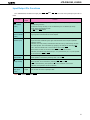
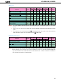
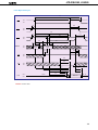
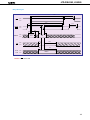
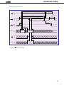
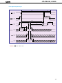
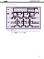
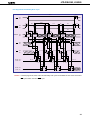
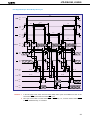
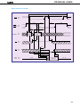
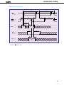
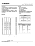
µ PD42S4260, 424260
AC Characteristics
(Recommended Operating Conditions unless otherwise noted)
AC Characteristics Test Conditions
(1) Input timing specification
VIH
(2) Output timing specification
= 2.4 V
VOH (MIN.) = 2.4 V
VIL (MAX.) = 0.8 V
VOL (MAX.) = 0.4 V
(MIN.)
tT = 5 ns
tT = 5 ns
(3) Output load condition
VCC
1,660 Ω
I/O
100 pF
590 Ω
CL
Common to Read, Write, Read Modify Write Cycle
Parameter
Symbol
t RAC = 60 ns
t RAC = 70 ns
t RAC = 80 ns
MIN.
MAX.
MIN.
MAX.
MIN.
MAX.
Unit
Notes
Read/Write cycle time
t RC
110
–
130
–
150
–
ns
RAS precharge time
tRP
40
–
50
–
60
–
ns
CAS precharge time
t CPN
10
–
10
–
10
–
ns
RAS pulse width
t RAS
60
10,000
70
10,000
80
10,000
ns
CAS pulse width
t CAS
15
10,000
20
10,000
20
10,000
ns
RAS hold time
t RSH
15
–
20
–
20
–
ns
CAS hold time
t CSH
60
–
70
–
80
–
ns
RAS to CAS delay time
tRCD
20
45
20
50
20
60
ns
2
RAS to column address delay time
tRAD
15
30
15
35
15
40
ns
2
CAS to RAS precharge time
t CRP
10
–
10
–
10
–
ns
3
Row address setup time
t ASR
0
–
0
–
0
–
ns
Row address hold time
t RAH
10
–
10
–
10
–
ns
Column address setup time
t ASC
0
–
0
–
0
–
ns
Column address hold time
t CAH
15
–
15
–
15
–
ns
OE lead time referenced to RAS
t OES
0
–
0
–
0
–
ns
CAS to data setup time
t CLZ
0
–
0
–
0
–
ns
OE to data setup time
tOLZ
0
–
0
–
0
–
ns
OE to data delay time
tOED
15
–
15
–
20
–
ns
Masked byte write hold time referenced to RAS
t MRH
0
–
0
–
0
–
ns
tT
3
50
3
50
3
50
ns
t REF
–
128
–
128
–
128
ms
–
8
–
8
–
8
ms
Transition time (rise and fall)
Refresh time
µPD42S4260
µPD424260
1
4
8