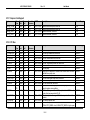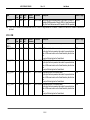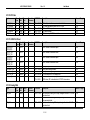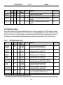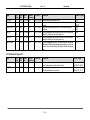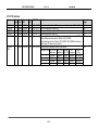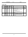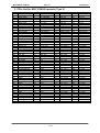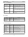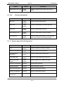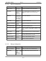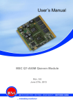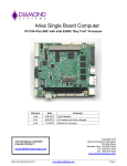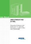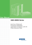
1
User Manual COM Express Basic Module MSC CXB-6S / CXB-6SI TM Type 2 Pin-out 2 / 3 Generation Intel Core™ Processor Family Intel® 6 / 7 Series Chipset nd rd ® Rev. 1.8 2015-04-15 MSC CXB-6S / CXB-6SI Rev. 1.8 User Manual Preface Copyright Notice Copyright © 2014 MSC Technologies GmbH. All rights reserved. Copying of this document, and giving it to others and the use or communication of the contents thereof, is forbidden without express authority. Offenders are liable to the payment of damages. All rights are reserved in the event of the grant of a patent or the registration of a utility model or design. Important Information This documentation is intended for qualified audience only. The product described herein is not an end user product. It was developed and manufactured for further processing by trained personnel. Disclaimer Although this document has been generated with the utmost care no warranty or liability for correctness or suitability for any particular purpose is implied. The information in this document is provided “as is” and is subject to change without notice. EMC Rules This unit has to be installed in a shielded housing. If not installed in a properly shielded enclosure, and used in accordance with the instruction manual, this product may cause radio interference in which case the user may be required to take adequate measures at his or her owns expense. Trademarks All used product names, logos or trademarks are property of their respective owners. Certification MSC Technologies GmbH is certified according to DIN EN ISO 9001:2000 standards. Life-Cycle-Management MSC products are developed and manufactured according to high quality standards. Our lifecycle-management assures long term availability through permanent product maintenance. Technically necessary changes and improvements are introduced if applicable. A productchange-notification and end-of-life management process assures early information of our customers. Product Support MSC engineers and technicians are committed to provide support to our customers whenever needed. Before contacting Technical Support of MSC Technologies GmbH, please consult the respective pages on our web site at www.msc-technologies.eu for the latest documentation, drivers and software downloads. If the information provided there does not solve your problem, please contact our Technical Support: Email: [email protected] Phone: +49 8165 906-200 2 / 81 MSC CXB-6S / CXB-6SI Rev. 1.8 User Manual Content 1 2 3 4 5 6 General Information ......................................................................................................................... 5 1.1 Revision History ........................................................................................................................ 5 1.2 Reference Documents............................................................................................................... 5 1.3 Introduction ............................................................................................................................... 6 Technical Description ....................................................................................................................... 7 2.1 Key features.............................................................................................................................. 7 2.2 Block diagram ........................................................................................................................... 8 2.3 COM Express implementation ................................................................................................... 9 2.4 Functional units........................................................................................................................10 2.5 Power Supply...........................................................................................................................11 2.6 Power Dissipation ....................................................................................................................11 2.6.1 Running Mode...................................................................................................................11 2.6.2 Power Dissipation (Standby Modes) ..................................................................................12 2.7 System Memory .......................................................................................................................13 2.8 Mechanical Dimensions ...........................................................................................................13 2.8.1 Compact module ...............................................................................................................13 2.9 Thermal specifications..............................................................................................................14 2.10 Signal description .................................................................................................................15 2.10.1 High Definition Audio.........................................................................................................15 2.10.2 Ethernet ............................................................................................................................16 2.10.3 IDE ...................................................................................................................................16 2.10.4 Serial ATA.........................................................................................................................17 2.10.5 PCI Express Lanes ...........................................................................................................18 2.10.6 PCI Express x16Graphic Lanes .........................................................................................18 2.10.7 Express Card Support .......................................................................................................19 2.10.8 PCI Bus ............................................................................................................................19 2.10.9 USB ..................................................................................................................................20 2.10.10 LPC Bus ...........................................................................................................................21 2.10.11 LVDS Flat Panel ...............................................................................................................21 2.10.12 Analog VGA ......................................................................................................................21 2.10.13 Digital Display Interfaces ...................................................................................................22 2.10.14 Miscellaneous ...................................................................................................................25 2.10.15 Power and System Management .......................................................................................26 2.10.16 General Purpose I/O .........................................................................................................27 2.10.17 SPI Interface .....................................................................................................................28 2.10.18 Module Type Definition......................................................................................................29 2.10.19 Power and GND ................................................................................................................30 2.11 Pin List for MSC CXB-6S module (Type 2) ............................................................................31 2.12 DDI Port Pin Assignment ......................................................................................................33 1) CTRLDATA pins do have strap functionality and are sampled during power up. A high level on these pins enables the appropriate DDI port B, C or D inside the PCH. ........................................................34 Jumpers and Connectors ................................................................................................................35 3.1 Jumpers...................................................................................................................................35 3.2 Fan Connector .........................................................................................................................36 Watchdog .......................................................................................................................................36 System resources ...........................................................................................................................37 5.1 PCI IRQ Routing ......................................................................................................................37 5.2 IRQ Lines in APIC Mode ..........................................................................................................38 5.3 Carrier Board PCI Resource Allocation.....................................................................................39 5.4 SMB Address Map ...................................................................................................................39 BIOS...............................................................................................................................................40 3 / 81 MSC CXB-6S / CXB-6SI Rev. 1.8 User Manual 6.1.6 The Main Menu .................................................................................................................43 6.1.7 The Advanced Menu .........................................................................................................45 6.1.9 Chipset .............................................................................................................................61 6.1.12 Boot ..................................................................................................................................71 6.1.13 Security.............................................................................................................................72 6.1.14 The Save & Exit Menu.......................................................................................................73 6.2 BIOS and Firmware Update .....................................................................................................74 6.5 Bios Recovery..........................................................................................................................76 6.7 Tech Notes ..............................................................................................................................77 7 EAPI ...............................................................................................................................................80 8 Troubleshooting ..............................................................................................................................81 4 / 81 MSC CXB-6S / CXB-6SI Rev. 1.8 User Manual 1 General Information 1.1 Revision History Rev. Date Description 1.0 2012-10-29 Final formatting; released version 1.1 2013-01-22 Minor changes 1.2 2013-05-28 Added additional information 1.3 2013-06-27 Added additional I2C bus information 1.4 2013-07-31 Format changed 1.5 2014-06-20 Block diagram updated 1.6 2014-09-04 New covering page 1.7 2014-12-23 Corrected Recovery Link 1.8 2015-04-15 Pull-up/-down description changed in chapter 2.10 1.2 Reference Documents [1] COM Express Module Base Specification COM Express Revision 2.0 Last update: August 8th, 2010 [2] PCI Local Bus Specification Rev. 2.1 PCI21.PDF Last update: June 1st, 1995 http://www.pcisig.com [3] ATA/ATAPI-6 Specification d1410r3b.pdf http://www.t13.org/ [4] Serial ATA Specification Serial ATA 1.0 gold.pdf Last update: August 29th, 2002 Rev.1.0 http://www.sata-io.org/ [5] IEEE Std. 802.3-2002 802.3-2002.pdf http://www.ieee.org [6] Universal Bus Specification usb_20.pdf Last update: April 27th, 2000 http://www.usb.org nd [7] 2 Generation Intel® Core™ Processor Family Mobile and Intel Celeron® Processor Family Mobile Datasheet, Volume 1 2nd-gen-core-family-mobile-vol-1-datasheet.pdf Last update: September 2011 http://www.intel.com/content/www/us/en/processors/core/CoreTechnicalResources.html [8] 2nd Generation Intel® Core™ Processor Family Mobile and Intel Celeron® Processor Family Mobile Datasheet, Volume 2 2nd-gen-core-family-mobile-vol-2-datasheet.pdf Last update: June 2011 http://www.intel.com/content/www/us/en/processors/core/CoreTechnicalResources.html [9] Mobile 3rd Generation Intel® Core™ Processor Family Datasheet – Volume 1 of 2 3rd-gen-core-family-mobile-vol-1-datasheet.pdf Last update: September 2012 http://www.intel.com/content/www/us/en/processors/core/CoreTechnicalResources.html [10] Mobile 3rd Generation Intel® Core™ Processor Family Datasheet – Volume 2 of 2 3rd-gen-core-family-mobile-vol-2-datasheet.pdf Last update: June 2012 http://www.intel.com/content/www/us/en/processors/core/CoreTechnicalResources.html 5 / 81 MSC CXB-6S / CXB-6SI Rev. 1.8 User Manual [11] Intel® 6 Series Chipset and Intel® C200 series Chipset Datasheet 6-chipset-c200-chipset-datasheet.pdf Last update: May 2011 http://www.intel.com/products/notebook/chipsets/6series/technicaldocuments.htm [12] Intel® 6 Series Chipset and Intel® C200 series Chipset Specification Update 6-and-c200-chipset-specification-update.pdf Last update: August 2011 http://www.intel.com/products/notebook/chipsets/6series/technicaldocuments.htm [13] Intel ® 7Series / C216 Chipset Family Platform Controller Hub (PCH) Datasheet 7-series-chipset-pch-datasheet.pdf Last update: June 2012 http://www.intel.com/content/www/us/en/chipsets/7-series-chipset-pchdatasheet.html?wapkw=intel+7+series+chipsets [14] Intel ® 7Series / C216 Chipset Family Platform Controller Hub (PCH) Family Specification Update 7-series-chipset-pch-spec-update.pdf Last update: August 2012 Revision 010 http://www.intel.com/content/www/us/en/chipsets/7-series-chipset-pch-specupdate.html?wapkw=intel+7+series+chipsets 1.3 Introduction COM Express™, an open specification of the PICMG (PCI Industrial Computer Manufacturer Group), is a module concept to bring PCI Express and other latest technologies like SATA, USB 2.0 and LVDS on a COM (Computer On Module). A COM Express™ module is plugged onto an application-specific base board similar to the ETX concept, but offers more options and a growth path to future CPU technologies. Utilizing different sizes, COM Express™ can be used for highly embedded solutions up to high performance platforms. The design of the MSC CXB-6S module supports the 2nd Generation Intel® Core Processor Family enabling you to boost your embedded application to highest performance levels. For evaluation and design-in of the COM Express™ modules we offer evaluation baseboards and develop motherboards providing the interface infrastructure for the COM Express™ module using PC type connectors for external access. Currently three module sizes are defined in the COM Express Specification 2.0: the Compact Module, Basic Module and the Extended Module. The primary difference between them is the over-all physical size and the performance envelope supported by each. The Extended Module is the largest and can support larger processor and memory solutions. The Basic Module is the most common supporting typical processor platforms in the embedded world. The Compact Module is the smallest one and is intended to be used when designing with processors and chipsets in small form factor footprints (SFF). All module sizes use the same connectors and pin-outs and utilize several common mounting hole positions. This level of compatibility allows that a carrier board designed to accommodate an Extended Module can also support a Basic or Compact Module. Up to 440 pins of connectivity are available between COM Express™ modules and the Carrier Board. Legacy buses such as PCI, parallel ATA, LPC, HDA are supported as well as new high speed serial interconnects such as PCI Express, Serial ATA and Gigabit Ethernet. To enhance interoperability between COM Express™ modules and Carrier Boards, seven common signaling configurations (Pin-out Types) have been defined to ease system integration. 6 / 81 MSC CXB-6S / CXB-6SI Rev. 1.8 User Manual 2 Technical Description 2.1 Key features The MSC CXB-6S COM Express module is designed as a type 2 module according to COM Express® Module Base Specification Revision 2.0 and is also drop in compatible with carrier boards designed according to COM Express® Base Specification R1.0. Key features include: Module size: 125 mm x 95 mm Various 2nd and 3rd Generation Intel® Core Processors Dual 220 pin connector (440 pins) 2x DDR3 SO-DIMM module up to 8 GB each one Eight USB 2.0 ports; 4 shared over-current lines Four Serial ATA ports with data rates up to 3.0Gb/s (300MB/s) Optional SATA NAND Flash Silicon Disk (4 GB to 32 GB) Five PCI Express x1 lanes Support pins for two ExpressCards Dual 24-bit LVDS channel Analog VGA High definition digital audio interface (external CODEC) Single Gbit Ethernet interface ( Intel 82579LM, Device ID 0x1502 ) with Wake On Lan support (S3,S4,S5) LPC interface Support for following Super IO : Winbond 83627 Four GPI pins Four GPO pins +12V primary power supply input +5V standby (optional) and 3.3V RTC power supply inputs 32 bit PCI interface IDE port (to support legacy ATA devices such as CD-ROM drives and Compact Flash storage cards) 21 PCI Express lanes (5 on A-B and 16 on C-D) 16 of 21 PCI Express lanes used for PCI Express Graphics Up to three digital display interfaces configurable as SDVO, HDMI, DVI or DisplayPort (pins shared with PCI Express Graphics) TPM module (option, TPM 1.2, SLB9635) Automatic fan control Watchdog timer Embedded Application Programming Interface (EAPI) 7 / 81 MSC CXB-6S / CXB-6SI Rev. 1.8 2.2 Block diagram 8 / 81 User Manual MSC CXB-6S / CXB-6SI Rev. 1.8 User Manual 2.3 COM Express implementation COM Express™ required and optional features of pin-out type 2 are summarized in the following table. The features identified as Minimum (Min.) shall be implemented by all modules. Features identified up to Maximum (Max) may be additionally implemented by a module. The column MSC CXB-6S shows the implemented features of the MSC module. Type 2 Min / Max MSC CXB-6S 0/1 1/6 1 5 (x1) signals are multiplexed with SDVO signals 6 (x1) as an option if no PCI bus is needed 0 / 16 1 (x16) off-module x16 PCI Express Graphics 0/2 0 /0 0/0 0/2 0/1 NA 1/1 1 3 3 2 1 0 1 SATA Ports 1/4 4/(1 x SSD) HDA Digital Interface USB 2.0 Ports USB Client Gbit LAN 0/1 4/8 0/1 1/1 1 8 0 1 PCI Bus - 32 Bit 1/1 1 Express Card Support LPC Bus SPI 1/2 1/1 1/2 2 1 2 System Management General Purpose Inputs General Purpose Outputs SMBus I2C Watch Dog Timer Speaker Out External BIOS ROM support Reset Functions 4/4 4/4 1/1 1/1 0/1 1/1 0/2 1/1 4 4 1 1 1 1 2 1 Power Management Thermal Protection Battery Low Alarm Suspend Wake Power Button Support Power Good 0/1 0/1 0/1 0/2 1/1 1/1 1 1 1 2 1 1 TPM 0/0 1 System I/O PCI Express Graphics (PEG) PCI Express Lanes 0 - 5 PCI Express Lanes 16-31 (same as PEG pins) SDVO Channels HDMI/DVI DisplayPort 1.1a LVDS Channels VGA Port TV-Out PATA Port 9 / 81 Note signals are multiplexed with PEG signals signals are multiplexed with PEG signals signals are multiplexed with PEG signals 1x dual channel, 2x24 Bit not available JMicron PCIe-PATA Controller JMB368 4x 300MB/s (ports 0 -3) optional 1 x Solid State Disk (port 4) Intel 82597LM GbE PHY Texas Instruments PCIe-to-PCI Bridge XIO2001 only one SPI flash is populated optional TPM 1.2 module MSC CXB-6S / CXB-6SI Rev. 1.8 User Manual 2.4 Functional units CPUs Intel® Core™ i7-3615QE (Quad Core, 2.3GHz, 6MB, SV 45W.) (FCBGA-1023) Intel® Core™ i7-3612QE (Quad Core, 2.1GHz, 6MB, SV 35W.) Intel® Core™ i7-3555LE (Dual Core, 2.5GHz, 4MB, LV 25W.) Intel® Core™ i7-3517UE (Dual Core, 2.1GHz, 4MB, ULV 17W.) Intel® Core™ i5-3610ME (Dual Core, 2.7GHz, 3MB, SV 35W.) Intel® Core™ i3-3120ME (Dual Core, 2.4GHz, 3MB, SV 35W.) Intel® Core™ i3-3217UE (Dual Core, 1.6GHz, 3MB, ULV 17W.) Intel® Core™ i7-2715QE (Quad Core, 2.1GHz, 6MB, SV 45W.) Intel® Core™ i7-2655LE (Dual Core, 2.1GHz, 4MB, LV 25W). Intel® Core™ i7-2610UE (Dual Core, 1.5GHz, 3MB, ULV 17W). Intel® Core™ i5-2515E (Dual Core, 2.1GHz, SV 35W). Intel® Core™ i3-2310E (Dual Core, 2.1GHz, SV 35W). Intel® Celeron® B810E (Dual Core, 1.6GHz, SV 35W). Intel® Celeron® 847E (Dual Core, 1.1GHz, 2MB, ULV 17W). Intel® Celeron® 827E (Single Core, 1.4GHz, 1.5MB, ULV 17W). Intel® Celeron® 807UE (Single Core, 1.0GHz, 1MB, ULV 10W). Chipset Intel® 82QM77 with Intel® Core™ i5-3 and Intel® Core™ i7-3 processor SKUs. Intel® 82QM76 with Intel® Core™ i3-3 processor SKUs. Intel® 82QM67 with Intel® Core™ i5-2 and Intel® Core™ i7-2 processor SKUs. Intel® 82HM65 with Intel® Core™ i3-2 and Intel® Celeron® processor SKUs. Memory Two 204-pin DDR3 SO-DIMM sockets for up to 16GB (4GB with Intel® Celeron® 807UE) non-ECC unbuffered DDR3 (One socket for up to 4GB on COM Express modules with Intel® Celeron® 807UE). Max. height 1250mil = 31.75mm. PC3-8500/ 10600 DDR3 SDRAM (DDR3-1066/1333). PC3-12800 DDR3 SDRAM (DDR3-1600) with Core i7-2715QE and Core i3/5/7-3. SATA 4 SATA channels up to 300MB/s each. EIDE 1 Enhanced IDE port ATA/UDMA100. USB 8 x USB 2.0. COM Express™ Type 2 interface, fully compliant to COM Express Base Specification R2.0. PCI Express™ Five channels PCIe x1. PCI 32 Bit standard interface. LPC Low Pin Count Bus for heritage interfaces. SPI Serial Peripheral Interface for up to two SPI flash devices. Graphics Controller Intel HD Graphics 2000/3000/4000 depending on processor SKU. Video Memory Intel® Dynamic Video Memory Technology (Intel® DVMT 5.0) LVDS Dual channel 24-bit LVDS (1.600 x 1.200 @ 60 Hz). Digital Display Ports DDPort B configurable as (multiplexed with HDMI/DVI (1920 x 1200 @ 60 Hz), DP (2560 x 1600 @ 60 Hz) and SDVO (200 PEG) MP/s). DDPort C configurable as HDMI/DVI (1920 x 1200 @ 60 Hz) and DP (2560 x 1600 @ 60 Hz). DDPort D configurable as HDMI/DVI (1920 x 1200 @ 60 Hz), DP (2560 x 1600 @ 60 Hz) and eDP . PEG PCIe x16 graphics port (PEG) supports external graphics cards (not available on Intel® Celeron® 807UE processor). CRT Interface 340.4 MHz RAMDAC (2.048 x 1.536 @ 75 Hz). Ethernet 10/100/1000Base-TX (Intel® 82579LM, Device ID 0x1502) with WOL support (S3,S4,S5). Sound Interface Intel® High Definition Audio Interface. Support for up to three external Codecs. Integrated DisplayPort/HDMI Audio support. Watchdog Timer PIC12C509A, creates system reset (programmable timeout, 1s … 255h). TPM (option) Optional TPM module, TPM 1.2, SLB9635. Fan Supply 4-pin header for support of a 12V PWM fan. Real Time Clock RTC integrated in PCH. 10 / 81 MSC CXB-6S / CXB-6SI Rev. 1.8 User Manual CMOS Battery External. System Monitoring Voltages, temperatures, fan Core voltage 3.3V onboard voltage 12V input voltage 5V SBY input voltage CPU temperature (0°C - 100°C) System memory temperature Board temperature Fan speed and automatic fan speed control 2.5 Power Supply +12V primary power supply input +5V standby Option, is not required for module operation. If not present, customer has to make sure that the supply voltages which are generated on the carrier board are switched off during suspend states, so that no current from the carrier board’s signal lines can flow to the CPU board. 3.3V RTC power supply Option, is not required for module operation. BIOS SETUP data is stored in a non volatile backup memory device, therefore configuration data will not get lost during power off (except for time and date information) Voltage Input range +12V +11.4V - 12.6 V +5V Standby +4.75V - 5.25 V +3V RTC power supply +2.0V - 3.3V Power Consumption Refer to chapter 2.6 Typ. 1.8 µA 2.6 Power Dissipation 2.6.1 Running Mode All measurements were made by plugging the module onto a MSC CX-EVA2 evaluation board. The module was equipped with two 4GByte memory modules NANYA NT4GC64B8HB0NS-CG 1112.CN, 4GB 2Rx8 PC3-10600S-9-10-F2.1333. The table below shows typical values which refer to consumption of the module itself without consumption of the base board and CPU fan. The following applications have been tested at room temperature. 1. DOS prompt. 2. Windows desktop (idle) under Microsoft Windows 7 Professional 64-bit SP1. 3. Running Intel® Thermal Analysis Tool (TAT!) Ver. 4.3 to achieve 70% CPU workload on each processor core/thread and 100% Graphics workload as recommended by Intel under Microsoft Windows 7 Professional 64-bit SP1. Module / CPU MSC CXB-6S-010 Intel® Celeron® 807UE (10W) MSC CXB-6S-009 Intel® Celeron® 827E (17W) MSC CXB-6S-008 Intel® Core™ i7-2715QE (45W) MSC CXB-6S-007 Intel® Core™ i7-2655LE (25W) MSC CXB-6S-006 Intel® Core™ i7-2610UE (17W) MSC CXB-6S-005 Intel® Core™ i5-2515E (35W) 11 / 81 Win 7 TAT! 1) long term max. DOS Win 7 Idle 11.5W 8W 19 W - 2) 13 W 8.5 W 25 W - 2) 19 W 9.5 W 64 W 75 W 17 W 8.5 W 41 W 47 W 18 W 8.5 W 30 W 36 W 20 W 9W 52 W 61 W MSC CXB-6S / CXB-6SI Rev. 1.8 User Manual MSC CXB-6S-004 19 W 8.5 W 47 W - 2) Intel® Core™ i3-2310E (35W) MSC CXB-6S-002 2) 12 W 8.5 W 28 W Intel® Celeron® 847E (17W) MSC CXB-6S-001 18 W 9W 40 W - 2) Intel® Celeron® B810E (35W) MSC CXB-6SI-011 14 W 9W 53 W 75 W Intel® Core™ i7-3612QE (35W) MSC CXB-6SI-008 14 W 12.5 W 65 W 76 W Intel® Core™ i7-3615QE (45W) MSC CXB-6SI-005 15 W 9W 51 W 58 W Intel® Core™ i5-3610ME (35W) nd 1) Due to the Intel® Turbo Boost Technology 2.0 feature on 2 Generation Intel® Core™ i5 and 2nd Generation Intel® Core™ i7 processors the maximum power consumption for short durations may be higher than the long term power consumption. The power supply must be able to deliver this additional amount of power. 2) The Intel® Turbo Boost Technology 2.0 feature is not available on 2nd Generation Intel® Core™ i3 and Intel® Celeron® processors. 2.6.2 Power Dissipation (Standby Modes) 1. System is shut down into “Soft Off” (S5) or “Suspend to Disk” (S4) by Windows 7 Professional 64-bit SP1. 2. System is shut down into “Soft Off” (S5) or “Suspend to Disk” (S4) by Windows 7 Professional 64bit SP1 with Wake On LAN enabled. 3. System is shut down into “Suspend to RAM” (S3) by Windows 7 Professional 64-bit SP1. 4. System is shut down into “Suspend to RAM” (S3) by Windows 7 Professional 64-bit SP1 with Wake On LAN enabled. Module / CPU S3 Input Power MSC CXB-6S-009 Intel® Celeron™ 827E (17W) 12V/5V_SBY MSC CXB-6S-004 Intel® Core™ i3-2310E (35W) MSC CXB-6S-001 Intel® Celeron™ B810E (35W) 12V only MSC CXB-6S-010 Intel® Celeron™ 807UE (10W) MSC CXB-6S-008 Intel® Core™ i7-2715QE (45W) 12V/5V_SBY MSC CXB-6S-006 Intel® Core™ i7-2610UE (17W) MSC CXB-6S-005 Intel® Core™ i5-2515E (35W) MSC CXB-6S-002 Intel® Celeron™ 847E (17W) 12V only MSC CXB-6S-007 Intel® Core™ i7-2655LE (25W) MSC CXB-6SI-011 Intel® Core™ i7-3612QE (35W) 12V/5V_SBY MSC CXB-6SI-008 Intel® Core™ i7-3615QE (45W) MSC CXB-6SI-005 12V only Intel® Core™ i5-3610ME (35W) 12 / 81 S4 / S5 no WOL WOL enabled no WOL WOL enabled 0.6 W 0.7 W 0.4 W 0.5 W 0.7 W 0.8 W 0.5 W 0.6 W 0.9 W 1.0 W 0.4 W 0.5 W 1.3 W 1.4 W 0.5 W 0.6 W 0.9 W 1.0 W 0.5 W 0.5 W 1.4 W 1.5 W 0.7 W 0.8 W MSC CXB-6S / CXB-6SI Rev. 1.8 User Manual 2.7 System Memory The MSC CXB-6S CPU module provides two sockets (only one socket on CXB-6S-010) for memory modules which have to meet the following demands: 204pin unbuffered non-ECC DDR3 SO-DIMM, Raw Card A, B, C and F. 1.5V Supply Voltage DDR3-1066 / PC3-8500, DDR3-1333 / PC3-10600 DDR3-1600 / PC3-12800 with Core i7-2715QE and Core i3/5/7-3. Maximum module height: 30mm. SPD (Serial Presence Detect) EEPROM. 2.8 Mechanical Dimensions 2.8.1 Compact module There are two height options defined in the COM Express specification : 5mm and 8mm. The height option is defined by the connectors on the baseboard. 13 / 81 MSC CXB-6S / CXB-6SI Rev. 1.8 User Manual 2.9 Thermal specifications The cooling solution of a COM Express module is based on a heat-spreader concept. A heat-spreader is a metal plate (typically aluminium) mounted on the top of the module. The connection between this plate and the module components is typically done by thermal interface materials like phase change foils, gap pads and copper or aluminium blocks. A very good thermal conductivity is required in order to conduct the heat from the CPU and the chipset to the heat-spreader plate. The heat-spreader of the MSC module is thermally attached using phase change materials and small aluminium blocks filling the gap between cpu and chipset dies and the heat-spreader plate. The heat-spreader is not a heat-sink! It is a defined thermal interface for the system designer with fixed mechanical dimensions, so it should be possible to change different module types without problems. There must be a cooling solution for the system. The surface temperature of the heat-spreader should not exceed 80°C. Main issue for the thermal functionality of a system is that each device of the module is operated within its specified thermal values. The max value for the CPU is 100°C and 108°C for the chipset. So there may be system implementations where the heat-spreader temperature could be higher. Anyway, in this case it has to be validated that there are no thermal specification violations of any assembled part or integrated circuit over the system temperature range even at worst case conditions. Additionally MSC offers adequate heat-sink solutions for the different CXB-6S modules depending on the power dissipation of the implemented CPU. For more information please refer to [email protected] or contact your sales representative. 14 / 81 MSC CXB-6S / CXB-6SI Rev. 1.8 User Manual 2.10 Signal description Pins are marked in the following tables with the power rail associated with the pin, and, for input and I/O pins, with the input voltage tolerance. The pin power rail and the pin input voltage tolerance may be different. For example, the PCI group is defined as having a 3.3V power rail, meaning that the output signals will only be driven to 3.3V, but the pins are tolerant of 5V signals. An additional label, “Sus”, indicates that the pin is active during suspend states (S3,S4,S5). If suspend modes are used, then care must be taken to avoid loading signals that are active during suspend to avoid excessive suspend mode current draw. I = Input. O = Output. OD = Open Drain output. I/OD = Bi-directional Input/Open Drain Output Pin. I/O = Bi-directional Input/Output. ePU = external pull-up resistor on COM Express module. ePD = external pull-down resistor on COM Express module. eSR = external series resistor on COM Express module. iPU = integrated pull-up resistor inside PCH or other IC, real value may vary from nominal one. iPD = integrated pull-down resistor inside PCH or other IC, real value may vary from nominal one. 2.10.1 High Definition Audio Signal HDA_RST# HDA_SYNC Pin Type O O Signal Level CMOS CMOS Power Remark / Rail Tolerance 3.3V Sus 3.3V Sus HDA_BITCLK HDA_SDOUT O O CMOS 3.3V Sus CMOS 3.3V Sus HDA_SDIN[0:2] I CMOS 3.3V Sus 3.3V PU/PD/SR Description Source / Target eSR = 33 Ω ePU =1 KΩ iPD = 20 KΩ eSR = 33 Ω eSR = 33 Ω iPD = 20 KΩ eSR = 33 Ω iPD = 20 KΩ eSR = 33 Ω Reset output to CODEC, active low. 48kHz fixed-rate, sample-synchronization signal to the CODEC(s), functional strap option sampled with rising edge of RSMRST#, iPD is disabled after RSMRST# de-assertion. 24.00 MHz serial data clock generated by the PCH Serial TDM data output to the CODEC, functional strap option, iPD is disabled after PLTRST# de-assertion. Do not pull high externally. Serial TDM data inputs from up to 3 CODECs. PCH PCH 15 / 81 PCH PCH PCH MSC CXB-6S / CXB-6SI Rev. 1.8 User Manual 2.10.2 Ethernet Signal GBE0_MDI[0:3]+ GBE0_MDI[0:3]- Pin Signal Power Remark / Type Level Rail Tolerance I/O Analog 3.3V Sus 3.3V GBE0_ACT# GBE0_LINK# GBE0_LINK100# GBE0_LINK1000# OD OD OD OD CMOS CMOS CMOS CMOS 3.3V Sus 3.3V Sus 3.3V Sus 3.3V Sus 5V / 20 mA 5V / 20 mA 5V / 20 mA 5V / 20 mA GBE0_CTREF REF IDE_D[0:6/8:15] IDE_D7 Pin Type I/O I/O Signal Level CMOS CMOS Power Rail 3.3V 3.3V Remark / Tolerance 3.3V 3.3V IDE_A[0:2] IDE_IOW# IDE_IOR# IDE_REQ O O O I CMOS CMOS CMOS CMOS 3.3V 3.3V 3.3V 3.3V 3.3V 3.3V 3.3V 3.3 V IDE_ACK# IDE_CS1# IDE_CS3# IDE_IORDY O O O I CMOS CMOS CMOS CMOS 3.3V 3.3V 3.3V 3.3V 3.3V 3.3V 3.3V 3.3 V IDE_RESET# IDE_IRQ O I CMOS 3.3V CMOS 3.3V 3.3V 3.3 V 2.10.3 PU/PD/SR Description Source / Target Gigabit Ethernet Controller 0: Media Dependent Interface Differential Pairs 0,1,2,3. The MDI can operate in 1000, 100 and 10 Mbit / sec modes. MDI[0]+/B1_DA+/MDI[1]+/B1_DB+/MDI[2]+/B1_DC+/MDI[3]+/B1_DD+/Gigabit Ethernet Controller 0 activity indicator, active low. Gigabit Ethernet Controller 0 link indicator, active low. Gigabit Ethernet Controller 0 100 Mbit / sec link indicator, active low. Gigabit Ethernet Controller 0 1000 Mbit / sec link indicator, active low. N/A. Center tab voltage not needed by 82759LM. 82579LMi PU/PD/SR Description Source / Target eSR = 33 Ω eSR = 33 Ω iPD = 32 k Ω eSR = 33 Ω eSR = 22 Ω eSR = 22 Ω ePD = 5.6 KΩ eSR = 82 Ω iPD = 32 KΩ eSR 22Ω eSR = 33 Ω eSR = 33 Ω ePU = 4.7 KΩ eSR = 82 Ω iPU = 47 KΩ eSR = 33 Ω ePD = 10 KΩ Bidirectional data to / from IDE device. Bidirectional data to / from IDE device. JMB368 JMB368 Address lines to IDE device. I/O write line to IDE device. Data latched on trailing (rising) edge. I/O read line to IDE device. IDE device DMA Request. Asserted by IDE device to request a data transfer. JMB368 JMB368 JMB368 JMB368 IDE Device DMA Acknowledge. IDE Device Chip Select for 1F0h to 1FFh range. IDE Device Chip Select for 3F0h to 3FFh range. IDE device I/O ready input. Pulled low by the IDE device to extend the cycle. JMB368 JMB368 JMB368 JMB368 Reset output to IDE device, active low. Interrupt request from IDE device. JMB368 JMB368 82579LM 82579LM 82579LM 82579LM IDE Signal 16 / 81 MSC CXB-6S / CXB-6SI Signal IDE_CBLID# Pin Signal Power Type Level Rail I CMOS 3.3V Remark / Tolerance 3.3 V Rev. 1.8 PU/PD/SR User Manual Description eSR = 82 Ω iPD = 32 KΩ ePD = 100 KΩ Input from off-module hardware indicating the type of IDE cable being used. High indicates a 40-pin cable used for legacy IDE modes. Low indicates that an 80-pin cable with interleaved grounds is used. Such a cable is required for Ultra-DMA 66, 100 and 133 modes. Note: The IDE interface is realized by a JMicron JMB368 PCIe-to-IDE controller located on PCIe lane #6. Source / Target JMB368 2.10.4 Serial ATA Signal SATA0_TX+ SATA0_TXSATA0_RX+ SATA0_RXSATA1_TX+ SATA1_TXSATA1_RX+ SATA1_RXSATA2_TX+ SATA2_TXSATA2_RX+ SATA2_RXSATA3_TX+ SATA3_TXSATA3_RX+ SATA3_RXATA_ACT# Pin Signal Power Type Level Rail O SATA 3.3V I SATA 3.3V O SATA 3.3V I SATA 3.3V O SATA 3.3V I SATA 3.3V O SATA 3.3V I SATA 3.3V OD CMOS 3.3V Remark / PU/PD/SR Tolerance AC coupled on module AC coupled on module AC coupled on module AC coupled on module AC coupled on module AC coupled on module AC coupled on module AC coupled on module 5V /20 mA Description Source / Target Serial ATA Channel 0 transmit differential pair. PCH Serial ATA Channel 0 receive differential pair. PCH Serial ATA Channel 1transmit differential pair. PCH Serial ATA Channel 1 receive differential pair. PCH Serial ATA Channel 2 transmit differential pair. PCH Serial ATA Channel 2 receive differential pair. PCH Serial ATA Channel 3 transmit differential pair. PCH Serial ATA Channel 3 receive differential pair. PCH SATA activity indicator, active low. PCH 17 / 81 MSC CXB-6S / CXB-6SI Rev. 1.8 User Manual 2.10.5 PCI Express Lanes Signal PCIE_TX[0:4+ PCIE_TX[0:4]PCIE_RX[0:4]+ PCIE_RX[0:4]PCIE_CLK_REF+ PCIE_CLK_REF- Pin Signal Power Type Level Rail O PCIe 3.3V I PCIe 3.3V O PCIe CLK 3.3V Remark / PU/PD/SR Tolerance AC coupled on module AC coupled off module Description Source / Target PCI Express Differential Transmit Pairs 0 through 4 PCH PCI Express Differential Receive Pairs 0 through 4 PCH Differential Reference Clock output for all PCI Express and PCI Express Graphics lanes. PCH Note: PCIe lanes #5 is used on the CXB-6S module and therefore not available for externally by default. 2.10.6 PCI Express x16Graphic Lanes Signal PEG_TX[0:15]+ PEG_TX[0:15]- Pin Signal Power Type Level Rail O PCIe 3.3V Remark / PU/PD/SR Tolerance AC coupled on module Description PCI Express Graphics transmit differential pairs. These signals can also be used as standard PCI Express transmit lanes as PCIE_TX[16:31]+/- on type 4 and type 5 modules. Some of them are multiplexed with the digital display interface of the PCH (SDVO, DVI, HDMI or DisplayPort). PEG_RX[0:15]+ I PCIe 3.3V AC coupled PCI Express Graphics receive differential pairs. PEG_RX[0:15]off module These signals can also be used as standard PCI Express receive lanes as PCIE_RX[16:31]+/- on type 5 and type 5 modules. Some of these signals are multiplexed with the digital display interface of the PCH (SDVO, DVI, HDMI or DisplayPort). PEG_RX5I/O CMOS 3.3V 3.3V iPD = 20 KΩ DDPC_CTRLDATA, strap option, Port C detect, iPD is disabled after PLTRST# de-assertion. PEG_RX8I/O CMOS 3.3V 3.3V iPD = 20 KΩ DDPD_CTRLDATA, strap option, Port D detect, iPD is disabled after PLTRST# de-assertion. PEG_LANE_RV# I CMOS 3.3V 3.3V ePU = 5.7 KΩ PCI Express Graphics lane reversal input strap. Pull low on the carrier board to reverse lane order. Be aware that the digital display interface that share this interface do not support reverse order functionality if this strap is low. PEG_ENABLE# I CMOS 3.3V 3.3V ePU = 10 KΩ PCI Express x16 external Graphics Enable Signal. Pull low to enable the x16 interface (PEG or PCIe). Pull high or leave as no connect to switch the PCHs digital display interface (port B, port C and port D) to the COM Express connector. Note: Module input signal PEG_ENABLE# (D97) must be low to select PEG/PCIe functionality. 18 / 81 Source / Target CPU CPU CPU CPU CPU PCH / MUX MSC CXB-6S / CXB-6SI Rev. 1.8 User Manual 2.10.7 Express Card Support Signal Pin Type I I O O Signal Level CMOS CMOS CMOS CMOS Power Rail 3.3V 3.3V 3.3V 3.3V Remark / Tolerance 3.3V 3.3V 3.3V 3.3V PU/PD Description Source / Target ePU = 10 KΩ ePU = 10 KΩ ePU = 8.2 KΩ ePU = 8.2 KΩ ExpressCard card request, active low ExpressCard card request, active low ExpressCard reset, active low ExpressCard reset, active low PCH PCH PCH PCH Pin Type I/O I/O I/O I/O I/O I/O I/O I/O I/O Signal Level CMOS CMOS CMOS CMOS CMOS CMOS CMOS CMOS CMOS Power Rail 3.3V 3.3V 3.3V 3.3V 3.3V 3.3V 3.3V 3.3V 3.3V Remark / Tolerance 5V 5V 5V 5V 5V 5V 5V 5V 5V PU/PD/SR Description Source / Target XIO2001 XIO2001 XIO2001 XIO2001 XIO2001 XIO2001 XIO2001 XIO2001 XIO2001 CMOS CMOS CMOS CMOS CMOS 3.3V 3.3V 3.3V 3.3V 3.3V 5V ePU = 8.2 KΩ 5V 5V ePU = 8.2 KΩ ePU = 8.2 KΩ PCI_PME# I O O I/O I/O OD I CMOS 3.3V Sus 5V ePU = 8.2 KΩ PCI_CLKRUN# I/O CMOS 3.3V 5V ePU = 8.2 KΩ PCI_IRQ[A:D]# PCI_CLK I O CMOS 3.3V CMOS 3.3V 5V ePU = 8.2 KΩ eSR = 82 Ω PCI bus multiplexed address and data lines PCI bus byte enable lines, active low PCI bus Device Select, active low. PCI bus Frame control line, active low. PCI bus Initiator Ready control line, active low. PCI bus Target Ready control line, active low. PCI bus STOP control line, active low, driven by cycle initiator. PCI bus parity Parity Error: An external PCI device drives PERR# when it receives data that has a parity error. PCI bus master request input lines, active low. PCI bus master grant output lines, active low. PCI Reset output, active low. PCI Lock control line, active low. System Error: SERR# may be pulsed active by any PCI device that detects a system error condition. PCI Power Management Event: PCI peripherals drive PME# to wake system from low-power states S1–S5. Bidirectional pin used to support PCI clock run protocol for mobile systems. PCI interrupt request lines. PCI clock output. 33 MHz if PCI_M66EN = low, 66 MHz if PCI_M66EN = high or open. EXCD[0]_CPPE# EXCD[1]_CPPE# EXCD[0]_RST# EXCD[1]_RST# 2.10.8 PCI Bus Signal PCI_AD[0:31] PCI_C/BE[0:3]# PCI_DEVSEL# PCI_FRAME# PCI_IRDY# PCI_TRDY# PCI_STOP# PCI_PAR PCI_PERR# PCI_REQ[0:3]# PCI_GNT[0:3]# PCI_RESET# PCI_LOCK# PCI_SERR# ePU = 8.2 KΩ ePU = 8.2 KΩ ePU = 8.2 KΩ ePU = 8.2 KΩ ePU = 8.2 KΩ ePU = 8.2 KΩ 19 / 81 XIO2001 XIO2001 XIO2001 XIO2001 XIO2001 XIO2001 XIO2001 XIO2001 XIO2001 MSC CXB-6S / CXB-6SI Signal Remark / Tolerance 5V PU/PD/SR Pin Signal Power Remark / Type Level Rail Tolerance I/O USB 3.3V Sus 3.3V PU/PD/SR I CMOS 3.3V Sus 3.3V ePU = 8.2 KΩ USB_2_3_OC# I CMOS 3.3V Sus 3.3V USB_4_5_OC# I CMOS 3.3V Sus 3.3V USB_6_7_OC# I CMOS 3.3V Sus 3.3V PCI_M66EN Pin Signal Power Type Level Rail I CMOS 3.3V Rev. 1.8 User Manual Description Source / Target ePU = 10 KΩ Module input signal indicates whether an off-module PCI device is XIO2001 capable of 66MHz operation. Pulled to GND by Carrier Board device or by Slot Card if the devices are NOT capable of 66 MHz operation. Note: The PCI bus is realized by a Texas Instruments XIO2001 PCIe-to-PCI bridge located on PCIe lane #5. Therefore PCIe lane #5 isn’t available for external use by default. 2.10.9 USB Signal USB[0:7]+ USB[0:7]USB_0_1_OC# Description Source / Target USB differential pairs, channels 0 through 7 PCH USB channels 0 and 1 over-current sense. A pull-up for this line is present on the module. An open drain driver from a USB current monitor on the Carrier Board may drive this line low. Do not pull this line high on the Carrier Board. ePU = 8.2 KΩ USB channels 2 and 3 over-current sense. A pull-up for this line is present on the module. An open drain driver from a USB current monitor on the Carrier Board may drive this line low. Do not pull this line high on the Carrier Board. ePU = 8.2 KΩ USB channels 4 and 5 over-current sense. A pull-up for this line is present on the module. An open drain driver from a USB current monitor on the Carrier Board may drive this line low. Do not pull this line high on the Carrier Board. ePU = 8.2 KΩ USB channels 6 and 7 over-current sense. A pull-up for this line is present on the module. An open drain driver from a USB current monitor on the Carrier Board may drive this line low. Do not pull this line high on the Carrier Board. 20 / 81 PCH PCH PCH PCH MSC CXB-6S / CXB-6SI Rev. 1.8 User Manual 2.10.10 LPC Bus Signal LPC_AD[0:3] LPC_FRAME# LPC_DRQ[0:1]# LPC_SERIRQ LPC_CLK Pin Type I/O O I I/OD O Signal Level CMOS CMOS CMOS CMOS CMOS Power Rail 3.3V 3.3V 3.3V 3.3V 3.3V Remark / Tolerance 3.3V PU/PD/SR Description Source / Target iPU = 20 KΩ 3.3V 3.3V iPU = 20 KΩ ePU = 200 Ω eSR = 22 Ω LPC multiplexed address, command and data bus LPC frame indicates the start of an LPC cycle LPC serial DMA request LPC serial interrupt LPC clock output - 33MHz nominal PCH PCH PCH PCH PCH Description Source / Target LVDS Channel A differential pairs PCH 2.10.11 LVDS Flat Panel Signal LVDS_A[0:3]+ LVDS_A[0:3]LVDS_A_CK+ LVDS_A_CKLVDS_B[0:3]+ LVDS_B[0:3]LVDS_B_CK+ LVDS_B_CKLVDS_VDD_EN LVDS_BKLT_EN LVDS_BKLT_CTRL LVDS_I2C_CK LVDS_I2C_DAT Pin Signal Power Type Level Rail O LVDS Remark / PU/PD/SR Tolerance O LVDS LVDS Channel A differential clock PCH O LVDS LVDS Channel B differential pairs PCH O LVDS LVDS Channel B differential clock PCH O O O O I/OD CMOS CMOS CMOS CMOS CMOS 3.3V 3.3V 3.3V 3.3V 3.3V 3.3V ePD = 100 KΩ LVDS panel power enable ePD = 100 KΩ LVDS panel backlight enable LVDS panel backlight brightness control ePU = 2.2 KΩ I2C clock output for LVDS display use ePU = 2.2 KΩ I2C data line for LVDS display use iPD = 20 KΩ LVDS detect, iPD is disabled after PLTRST# de-assertion. PCH PCH PCH PCH PCH 2.10.12 Analog VGA Signal VGA_RED Pin Signal Power Type Level Rail O Analog Remark / Tolerance PU/PD/SR Description Source / Target ePD = 150 Ω Red for monitor. Analog DAC output, designed to drive a 37.5-Ohm equivalent load. Green for monitor. Analog DAC output, designed to drive a 37.5Ohm equivalent load. Blue for monitor. Analog DAC output, designed to drive a 37.5-Ohm equivalent load. PCH VGA_GRN O Analog ePD = 150 Ω VGA_BLU O Analog ePD = 150 Ω 21 / 81 PCH PCH MSC CXB-6S / CXB-6SI Signal VGA_HSYNC VGA_VSYNC VGA_I2C_CK Pin Type O O O Signal Level CMOS CMOS CMOS Power Rail 3.3V 3.3V 3.3V VGA_I2C_DAT I/OD CMOS 3.3V Remark / Tolerance 3.3V Rev. 1.8 PU/PD/SR User Manual Description Horizontal sync output to VGA monitor Vertical sync output to VGA monitor 2 ePU = 2.2 KΩ DDC clock line. I C port dedicated to identify VGA monitor capabilities ePU = 2.2 KΩ DDC data line. I2C port dedicated to identify VGA monitor capabilities Source / Target PCH PCH PCH PCH 2.10.13 Digital Display Interfaces The Intel Platform Controller Hub (PCH) provides three Digital Display Ports B, C and D that may be configured for SDVO, HDMI, DVI or DisplayPort functionality. These ports may be switched to the COM Express Connector C-D by a HIGH level on input signal PEG_ENABLE# (D97) instead of the CPUs PCI Express Graphic lanes. The pin-out is chosen in a way that the digital display ports are accessible through special ADD2-Cards that can be plugged into the PEG slot on existing COM Express type 2 carrier boards. Be aware that the digital display interface does not support reverse order functionality if PEG_LANE_RV# strap is low. 2.10.13.1 SVDO (Digital Display Port B only) Signal SDVOB_RED+ SDVOB_REDSDVOB_GRN+ SDVOB_GRNSDVOB_BLU+ SDVOB_BLUSDVOB_CK+ SDVOB_CKSDVO_TVCLKIN+ SDVO_TVCLKINSDVO_INT+ SDVO_INTSDVO_FLDSTALL+ SDVO_FLDSTALL SDVO_CTRLDATA Pin Signal Power Type Level Rail O PCIe Remark / PU/PD/SR Tolerance AC coupled on module AC coupled on module AC coupled on module AC coupled on module AC coupled off module AC coupled off module AC coupled off module 3.3V iPD = 20 KΩ Description Serial Digital Video B red output differential pair Multiplexed with PEG_TX[0]+ and PEG_TX[0]O PCIe Serial Digital Video B green output differential pair Multiplexed with PEG_TX[1]+ and PEG_TX[1]O PCIe Serial Digital Video B blue output differential pair Multiplexed with PEG_TX[2]+ and PEG_TX[2]O PCIe Serial Digital Video B clock output differential pair. Multiplexed with PEG_TX[3]+ and PEG_TX[3]I PCIe Serial Digital Video B TVOUT Synchronization Clock input differential pair. Multiplexed with PEG_RX[0]+ and PEG_RX[0]I PCIe Serial Digital Video Interrupt input differential pair. Multiplexed with PEG_RX[1]+ and PEG_RX[1]I PCIe Serial Digital Video Field Stall input differential pair. Multiplexed with PEG_RX[2]+ and PEG_RX[2]I/O CMOS 3.3V SDVO Control Data. Shared with port B HDMI/DVI, strap option, Port B detect, iPD is disabled after PLTRST# de-assertion. SDVO_CTRLCLK I/O CMOS 3.3V 3.3V SDVO Control Clock. Shared with port B HDMI/DVI Note: PEG_ENABLE# (D97) from the carrier board must be high to select SDVO. 22 / 81 Source / Target PCH PCH PCH PCH PCH PCH PCH PCH PCH MSC CXB-6S / CXB-6SI 2.10.13.2 Rev. 1.8 User Manual DVI / HDMI Signal TMDSB_D[0:3]+ TMDSB_D[0:3]TMDSB_CTRLCLK Pin Signal Power Type Level Rail O TMDS Remark / PU/PD/SR Tolerance AC coupled on module 3.3V Description Source / Target PCH Port B HDMI/DVI Data [0:3] output differential pairs. Multiplexed with PEG_TX[0:3]+ and PEG_TX[0:3]I/O CMOS 3.3V Port B HDMI/DVI Control Clock. Shared with port B PCH SDVO_CTRLCLK TMDSB_CTRLDATA I/O CMOS 3.3V 3.3V iPD = 20 KΩ Port B HDMI/DVI Control Data. Shared with port B PCH SDVO_CTRLDATA, strap option, Port B detect, iPD is disabled after PLTRST# de-assertion. TMDSB_HPD I CMOS 3.3V 3.3V Port B HDMI/DVI Hot Plug Detect. PCH Multiplexed with PEG_RX3+ TMDSC_D[0:3]+ O TMDS AC coupled Port C HDMI/DVI Data [0:3] output differential pairs. PCH TMDSC_D[0:3]on module Multiplexed with PEG_TX[4:7]+ and PEG_TX[4:7]TMDSC_CTRLCLK I/O CMOS 3.3V 3.3V Port C HDMI/DVI Control Clock. PCH Multiplexed with PEG_RX5+ TMDSC_CTRLDATA I/O CMOS 3.3V 3.3V iPD = 20 KΩ Port C HDMI/DVI Control Data. Multiplexed with PEG_RX5PCH strap option, Port C detect, iPD is disabled after PLTRST# de-assertion. DDPC_HPD I CMOS 3.3V 3.3V Port C HDMI/DVI Hot Plug Detect. PCH Multiplexed with PEG_RX7+ TMDSD_D[0:3]+ O TMDS AC coupled Port D HDMI/DVI Data [0:3] output differential pairs. PCH TMDSD_D[0:3]on module Multiplexed with PEG_TX[8:11]+ and PEG_TX[8:11]TMDSD_CTRLCLK I/O CMOS 3.3V 3.3V Port D HDMI/DVI Control Clock. PCH Multiplexed with PEG_RX8+ TMDSD_CTRLDATA I/O CMOS 3.3V 3.3V iPD = 20 KΩ Port D HDMI/DVI Control Data. Multiplexed with PEG_RX8PCH strap option, Port D detect, iPD is disabled after PLTRST# de-assertion. TMDSD_HPD I CMOS 3.3V 3.3V Port D HDMI/DVI Hot Plug Detect. PCH Multiplexed with PEG_RX11+ Notes: PEG_ENABLE# (D97) from the carrier board must be high to select HDMI or DVI instead of PEG. Additional level shifters are required on the carrier board or ADD-2 card in order to translate TMDS data outputs into DVI / HDMI signal format. Video BIOS supports only SDVO on digital display port B. Please ask your MSC representative if other options are required on port B. 23 / 81 MSC CXB-6S / CXB-6SI 2.10.13.3 User Manual DisplayPort Signal DPB_LANE[0:3]+ DPB_LANE[0:3]DPB_AUX+ DPB_AUXDPB_HPD Pin Signal Power Type Level Rail O I/O I DPC_LANE[0:3]+ DPC_LANE[0:3]DPC_AUX+ DPC_AUXDPC_HPD O DPD_LANE[0:3]+ DPD_LANE[0:3]DPD_AUX+ DPD_AUXDPD_HPD O Note: Rev. 1.8 CMOS I/O I CMOS I/O I CMOS PEG_ENABLE# (D97) from Remark / PU/PD/SR Tolerance AC coupled on module AC coupled on module 3.3V Description Port B DisplayPort Lane [0:3] differential pairs. Multiplexed with PEG_TX[0:3]+ and PEG_TX[0:3]Port B DisplayPort Aux control channel differential pair Multiplexed with PEG_RX4+ and PEG_RX43.3V Port B DisplayPort Hot Plug Detect. Multiplexed with PEG_RX3+ AC coupled Port C DisplayPort Lane [0:3] differential pairs. on module Multiplexed with PEG_TX[4:7]+ and PEG_TX[4:7]AC coupled Port B DisplayPort Aux control channel differential pair on module Multiplexed with PEG_RX6+ and PEG_RX63.3V 3.3V Port C DisplayPort Hot Plug Detect. Multiplexed with PEG_RX7+ AC coupled Port D DisplayPort Lane [0:3] differential pairs. on module Multiplexed with PEG_TX[8:11]+ and PEG_TX[8:11]AC coupled Port D DisplayPort Aux control channel differential pair on module Multiplexed with PEG_RX10+ and PEG_RX103.3V 3.3V Port D DisplayPort Hot Plug Detect. Multiplexed with PEG_RX11+ the carrier board must be high to select DisplayPort instead of PEG. 24 / 81 Source / Target PCH PCH PCH PCH PCH PCH PCH PCH PCH MSC CXB-6S / CXB-6SI Rev. 1.8 User Manual 2.10.14 Miscellaneous Signal I2C_CK I2C_DAT SPKR BIOS_DIS[1:0]# WDT KBD_RST# Pin Signal Power Type Level Rail I/O CMOS 3.3V OD (3.3V Sus) I/O CMOS 3.3V OD (3.3V Sus) O CMOS 3.3V I CMOS 3.3V O CMOS 3.3V I CMOS 3.3V Remark / Tolerance 3.3V PU/PD/SR Description Source / Target ePU = 2.2 KΩ General purpose I2C port clock output PCH GPIO47 ePU = 2.2 KΩ General purpose I2C port data I/O line PCH GPIO56 Output for audio enunciator - the "speaker" in PC-AT systems PCH Module BIOS disable inputs [1:0]# PCH Active high output indicating that a watchdog time-out has occurred. PIC12F509 3.3V Input to module from (optional) external keyboard controller that can PCH force a reset. Pulled high on the module. This is a legacy artifact of the PC-AT. KBD_A20GATE I CMOS 3.3V 3.3V ePU = 10 KΩ Input to module from (optional) external keyboard controller that can PCH be used to control the CPU A20 gate line. The A20GATE restricts the memory access to the bottom megabyte and is a legacy artifact of the PC- AT. Pulled high on the module. Note: COM Express Specification R2.1 redefines the I2C bus to be in the suspend plane 3.3V_SUS rather than in the 3.3V plane. To avoid leakage current into carrier boards that were designed upon earlier COM Express specifications the MSC CXB-6S modules hold these pins in the 3.3V-plane. Alternatively the I2C bus can be switched to the 3.3V_SUS plane as an assembly option. Please contact your MSC representative if you will need this option. The I2C pins are implemented by bit banging at GPIOs. As a result, the maximal I2C bus speed depends on CPU performance. ePU = 5 KΩ ePD = 10 KΩ ePU = 10 KΩ 25 / 81 MSC CXB-6S / CXB-6SI Rev. 1.8 User Manual 2.10.15 Power and System Management Signal SYS_RESET# Pin Signal Power Remark / PU/PD/SR Type Level Rail Tolerance I CMOS 3.3V Sus 3.3V ePU = 10 KΩ iPU = 20 KΩ I CMOS 3.3V 3.3V ePU = 10 KΩ CB_RESET# O CMOS 3.3V PWR_OK I CMOS 3.3V Sus 3.3V SUS_STAT# SUS_S3# SUS_S4# SUS_S5# O O O O CMOS CMOS CMOS CMOS WAKE0# WAKE1# I I CMOS 3.3V Sus 3.3V CMOS 3.3V Sus 3.3V PWRBTN# 3.3V Sus 3.3V Sus 3.3V Sus 3.3V Sus 3.3V 3.3V 3.3V 3.3V 3.3V Description Power button to bring system out of or into Suspend states, active on falling edge after 16 ms debounce. Reset button input. When the SYS_RESET# pin is detected as active after the 16 ms debounce logic, the ICH attempts to perform a “graceful” reset, by waiting up to 25 ms for the SMBus to go idle. If the SMBus is idle when the pin is detected active, the reset occurs immediately; otherwise, the counter starts. If at any point during the count the SMBus goes idle the reset occurs. If, however, the counter expires and the SMBus is still active, a reset is forced upon the system even though activity is still occurring. Once the reset is asserted, it remains asserted for 5 to 6 ms regardless of whether the SYS_RESET# input remains asserted or not. It cannot occur again until SYS_RESET# has been detected inactive after the debounce logic, and the system is back to a full S0 state. This behavior is a result of Intel ICH internal chipset logic which is different to the COM Express Module Base Specification stating that the system shall remain in reset as long as SYS_RESET# input is low. eSR = 22 Ω Reset output from module to Carrier Board. Active low. Issued by module chipset and may result from a low SYS_RESET# input, a low PWR_OK input, a VCC_12V power input that falls below the minimum specification, a watchdog timeout, or may be initiated by the module software. ePU = 220 KΩ Power OK from main power supply. A high value indicates that the power is good. Indicates imminent suspend operation; used to notify LPC devices. Indicates system is in Suspend to RAM state. Active low output. Indicates system is in Suspend to Disk state. Active low output. Indicates system is in Soft Off state. Also known as "PS_ON" and can be used to control an ATX power supply. ePU = 1.2 KΩ PCI Express wake up signal. ePU = 10 KΩ General purpose wake up signal. May be used to implement wakeup on PS2 keyboard or mouse activity. 26 / 81 Source / Target PCH PCH PCH Power Good logic PCH PCH PCH PCH PCH PCH GPIO13 MSC CXB-6S / CXB-6SI Signal BATLOW# THRM# Pin Type I I Signal Level CMOS CMOS THERMTRIP# OD CMOS 3.3V SMB_CK I/O OD I/O OD I CMOS 3.3V Sus 3.3V ePU = 2.2 KΩ CMOS 3.3V Sus 3.3V ePU = 2.2 KΩ CMOS 3.3V Sus 3.3V ePU = 10 KΩ SMB_DAT SMB_ALERT# Power Rail 3.3V Sus 3.3V Rev. 1.8 Remark / PU/PD/SR Tolerance 3.3V ePU = 8.2 KΩ 3.3V ePU = 10 KΩ 3.3V ePU = 330 Ω User Manual Description Source / Target Indicates that external battery is low. Input from off-module temperature sensor indicating an over-temp situation. Active low output indicating that the CPU has entered thermal shutdown. System Management Bus bidirectional clock line. Power sourced through 5V standby rail and main power rails. System Management Bus bidirectional data line. Power sourced through 5V standby rail and main power rails. System Management Bus Alert – active low input can be used to generate an SMI# (System Management Interrupt) or to wake the system. Power sourced through 5V standby rail and main power rails. PCH PCH GPIO0 CPU, PCH PCH PCH PCH 2.10.16 General Purpose I/O Signal GPI[0:3] Pin Signal Power Type Level Rail I CMOS 3.3V GPO[0:3] O CMOS 3.3V Remark / Tolerance 3.3V PU/PD/SR Description Source / Target ePU = 10 KΩ General purpose output pins. Upon a hardware reset, these outputs are low. General purpose input pins. Pulled high internally on the module. PCH GPIO[38, 39, 48, 49] PCH GPIO[24, 35, 70, 71] 27 / 81 MSC CXB-6S / CXB-6SI Rev. 1.8 User Manual 2.10.17 SPI Interface Signal Pin Type SPI_CS# O SPI_MISO I SPI_MOSI O SPI_CLK O SPI_POWER O Signal Level CMOS CMOS CMOS CMOS Power BIOS_DIS [1:0]# CMOS 3.3V Sus 3.3V I Power Rem. PU/PD/SR Rail / Tol. 3.3V Sus ePU = 10 KΩ 3.3V Sus 3.3V eSR = 47 Ω 3.3V Sus eSR = 47 Ω 3.3V Sus eSR = 47 Ω 3.3V Sus Description Source / Target Chip select for Carrier Board SPI - may be sourced from chipset SPI0 or SPI1. PCH Data in to Module from Carrier SPI. PCH Data out from Module to Carrier SPI. PCH Clock from Module to Carrier SPI. PCH Power supply for Carrier Board SPI – sourced from Module – nominally 3.3V. The PCH Module shall provide a minimum of 100mA on SPI_POWER. Carriers shall use less than 100mA of SPI_POWER. SPI_POWER shall only be used to power SPI devices on the Carrier. ePU = 10 KΩ Selection straps to determine the BIOS boot device. PCH BIOS_DIS[1:0]# SPI_CS1# SPI_CS0# Carrier SPI BIOS Destination Destination SPI_CS# Descriptor Entry 1 1 Module Module HIGH Module SPI0/SPI1 1 0 Module Module HIGH Module Carrier FWH 0 1 Module Carrier SPI0 Carrier SPI0/SPI1 0 0 Carrier Module SPI1 Module SPI0/SPI1 28 / 81 MSC CXB-6S / CXB-6SI Rev. 1.8 User Manual 2.10.18 Module Type Definition Signal TYPE[0:2]# Pin Signal Power Remark / Type Level Rail Tolerance O On Type 2 module, all Type Detect pins are n.c. PU/PD/SR Description The TYPE pins indicate to the Carrier Board the Pin-out Type that is implemented on the module. The pins are tied on the module to either ground (GND) or are no-connects (NC). For Pin-out Type 1, these pins are don’t care (X). TYPE2# X NC NC NC NC GND TYPE10# O On COMX Rev 2.1 Type 2 modules this pin is n.c. Source / Target TYPE1# TYPE0# X X NC NC NC GND GND NC GND GND NC NC Carrier board logic Pin-out Type 1 Pin-out Type 2 Pin-out Type 3 (no IDE) Pin-out Type 4 (no PCI) Pin-out Type 5 (no IDE, no PCI) Pin-out Type 6 (no IDE, no PCI) The Carrier Board should implement combinatorial logic that monitors the module TYPE pins and keeps power off (e.g deactivates the ATX_ON signal for an ATX power supply) if an incompatible module pin- out type is detected. The Carrier Board logic may also implement a fault indicator such as a LED. Dual use pin. Carrier board logic Indicates to the Carrier Board that a Type 10 Module is installed. Indicates to the Carrier that a Rev 1.0/2.0 Module is installed TYPE10# NC Pin-out R2.0 PD Pin-out Type 10 pull down to ground with 4.7K resistor 12V Pin-out R1.0 This pin is reclaimed from the VCC_12V pool. In R1.0 Modules this pin will connect to other VCC_12V pins. In R2.0 this pin is defined as a no connect for types 1-6. A Carrier can detect a R1.0 Module by the presence of 12V on this pin. R2.0 Module types 1-6 will no connect this pin. Type 10 Modules shall pull this pin to ground through a 4.7K resistor. 29 / 81 MSC CXB-6S / CXB-6SI Rev. 1.8 User Manual 2.10.19 Power and GND Signal Description Source / Target VCC_12V Pin Signal Power Remark / PU/PD/SR Type Level Rail Tolerance Power 12V (±5%) Primary power input: +12V (±5%) VCC_5V_SBY Power VCC_RTC GND Power Power Standby power input: +5.0V (±5%) If VCC5_SBY is used, all available VCC_5V_SBY pins on the connector(s) shall be used. Only used for standby and suspend functions. May be left unconnected if these functions are not used in the system design. Real-time clock circuit-power input : +3.0V (+2.0V to +3.3V) Ground - DC power and signal and AC signal return path. All available GND connector pins shall be used and tied to Carrier Board GND plane. Voltage Regulators VCC3.3V SUS regulator 5V (±5%) 30 / 81 PCH MSC CXB-6S / CXB-6SI Rev. 1.8 User Manual 2.11 Pin List for MSC CXB-6S module (Type 2) Row A A1 A2 A3 A4 A5 A6 A7 A8 A9 A10 A11 A12 A13 A14 A15 A16 A17 A18 A19 A20 A21 A22 A23 A24 A25 A26 A27 A28 A29 A30 A31 A32 A33 A34 A35 A36 A37 A38 A39 A40 A41 A42 A43 A44 A45 A46 A47 A48 A49 A50 GND (FIXED) GBE0_MDI3GBE0_MDI3+ GBE0_LINK100# GBE0_LINK1000# GBE0_MDI2GBE0_MDI2+ GBE0_LINK# GBE0_MDI1GBE0_MDI1+ GND (FIXED) GBE0_MDI0GBE0_MDI0+ GBE0_CTREF SUS_S3# SATA0_TX+ SATA0_TXSUS_S4# SATA0_RX+ SATA0_RXGND (FIXED) SATA2_TX+ SATA2_TXSUS_S5# SATA2_RX+ SATA2_RXBATLOW# (S)ATA_ACT# AC/HDA_SYNC AC/HDA_RST# GND (FIXED) AC/HDA_BITCLK AC/HDA_SDOUT BIOS_DIS0# THRMTRIP# USB6USB6+ USB_6_7_OC# USB4USB4+ GND (FIXED) USB2USB2+ USB_2_3_OC# USB0USB0+ VCC_RTC EXCD0_PERST# EXCD0_CPPE# LPC_SERIRQ Row B B1 B2 B3 B4 B5 B6 B7 B8 B9 B10 B11 B12 B13 B14 B15 B16 B17 B18 B19 B20 B21 B22 B23 B24 B25 B26 B27 B28 B29 B30 B31 B32 B33 B34 B35 B36 B37 B38 B39 B40 B41 B42 B43 B44 B45 B46 B47 B48 B49 B50 GND (FIXED) GBE0_ACT# LPC_FRAME# LPC_AD0 LPC_AD1 LPC_AD2 LPC_AD3 LPC_DRQ0# LPC_DRQ1# LPC_CLK GND (FIXED) PWRBTN# SMB_CK SMB_DAT SMB_ALERT# SATA1_TX+ SATA1_TXSUS_STAT# SATA1_RX+ SATA1_RXGND (FIXED) SATA3_TX+ SATA3_TXPWR_OK SATA3_RX+ SATA3_RXWDT AC/HDA_SDIN2 AC/HDA_SDIN1 AC/HDA_SDIN0 GND (FIXED) SPKR I2C_CK I2C_DAT THRM# USB7USB7+ USB_4_5_OC# USB5USB5+ GND (FIXED) USB3USB3+ USB_0_1_OC# USB1USB1+ EXCD1_PERST# EXCD1_CPPE# SYS_RESET# CB_RESET# 31 / 81 Row C C1 C2 C3 C4 C5 C6 C7 C8 C9 C10 C11 C12 C13 C14 C15 C16 C17 C18 C19 C20 C21 C22 C23 C24 C25 C26 C27 C28 C29 C30 C31 C32 C33 C34 C35 C36 C37 C38 C39 C40 C41 C42 C43 C44 C45 C46 C47 C48 C49 C50 GND (FIXED) IDE_D7 IDE_D6 IDE_D3 IDE_D15 IDE_D8 IDE_D9 IDE_D2 IDE_D13 IDE_D1 GND (FIXED) IDE_D14 IDE_IORDY IDE_IOR# PCI_PME# PCI_GNT2# PCI_REQ2# PCI_GNT1# PCI_REQ1# PCI_GNT0# GND (FIXED) PCI_REQ0# PCI_RESET# PCI_AD0 PCI_AD2 PCI_AD4 PCI_AD6 PCI_AD8 PCI_AD10 PCI_AD12 GND (FIXED) PCI_AD14 PCI_C/BE1# PCI_PERR# PCI_LOCK# PCI_DEVSEL# PCI_IRDY# PCI_C/BE2# PCI_AD17 PCI_AD19 GND (FIXED) PCI_AD21 PCI_AD23 PCI_C/BE3# PCI_AD25 PCI_AD27 PCI_AD29 PCI_AD31 PCI_IRQA# PCI_IRQB# Row D D1 D2 D3 D4 D5 D6 D7 D8 D9 D10 D11 D12 D13 D14 D15 D16 D17 D18 D19 D20 D21 D22 D23 D24 D25 D26 D27 D28 D29 D30 D31 D32 D33 D34 D35 D36 D37 D38 D39 D40 D41 D42 D43 D44 D45 D46 D47 D48 D49 D50 GND (FIXED) IDE_D5 IDE_D10 IDE_D11 IDE_D12 IDE_D4 IDE_D0 IDE_REQ IDE_IOW# IDE_ACK# GND (FIXED) IDE_IRQ IDE_A0 IDE_A1 IDE_A2 IDE_CS1# IDE_CS3# IDE_RESET# PCI_GNT3# PCI_REQ3# GND (FIXED) PCI_AD1 PCI_AD3 PCI_AD5 PCI_AD7 PCI_C/BE0# PCI_AD9 PCI_AD11 PCI_AD13 PCI_AD15 GND (FIXED) PCI_PAR PCI_SERR# PCI_STOP# PCI_TRDY# PCI_FRAME# PCI_AD16 PCI_AD18 PCI_AD20 PCI_AD22 GND (FIXED) PCI_AD24 PCI_AD26 PCI_AD28 PCI_AD30 PCI_IRQC# PCI_IRQD# PCI_CLKRUN# PCI_M66EN PCI_CLK MSC CXB-6S / CXB-6SI Row A A51 A52 A53 A54 A55 A56 A57 A58 A59 A60 A61 A62 A63 A64 A65 A66 A67 A68 A69 A70 A71 A72 A73 A74 A75 A76 A77 A78 A79 A80 A81 A82 A83 A84 A85 A86 A87 A88 A89 A90 A91 A92 A93 A94 A95 A96 A97 A98 A99 A100 A101 A102 A103 A104 A105 A106 A107 A108 A109 A110 GND (FIXED) PCIE_TX5+ PCIE_TX5GPI0 PCIE_TX4+ PCIE_TX4GND PCIE_TX3+ PCIE_TX3GND (FIXED) PCIE_TX2+ PCIE_TX2GPI1 PCIE_TX1+ PCIE_TX1GND GPI2 PCIE_TX0+ PCIE_TX0GND (FIXED) LVDS_A0+ LVDS_A0LVDS_A1+ LVDS_A1LVDS_A2+ LVDS_A2LVDS_VDD_EN LVDS_A3+ LVDS_A3GND (FIXED) LVDS_A_CK+ LVDS_A_CKLVDS_I2C_CK LVDS_I2C_DAT GPI3 KBD_RST# KBD_A20GATE PCIE0_CK_REF+ PCIE0_CK_REFGND (FIXED) SPI_POWER SPI_MISO GPO0 SPI_CLK SPI_MOSI GND TYPE10# RSVD RSVD GND (FIXED) RSVD RSVD RSVD VCC_12V VCC_12V VCC_12V VCC_12V VCC_12V VCC_12V GND (FIXED) Rev. 1.8 Row B B51 B52 B53 B54 B55 B56 B57 B58 B59 B60 B61 B62 B63 B64 B65 B66 B67 B68 B69 B70 B71 B72 B73 B74 B75 B76 B77 B78 B79 B80 B81 B82 B83 B84 B85 B86 B87 B88 B89 B90 B91 B92 B93 B94 B95 B96 B97 B98 B99 B100 B101 B102 B103 B104 B105 B106 B107 B108 B109 B110 GND (FIXED) PCIE_RX5+ PCIE_RX5GPO1 PCIE_RX4+ PCIE_RX4GPO2 PCIE_RX3+ PCIE_RX3GND (FIXED) PCIE_RX2+ PCIE_RX2GPO3 PCIE_RX1+ PCIE_RX1WAKE0# WAKE1# PCIE_RX0+ PCIE_RX0GND (FIXED) LVDS_B0+ LVDS_B0LVDS_B1+ LVDS_B1LVDS_B2+ LVDS_B2LVDS_B3+ LVDS_B3LVDS_BKLT_EN GND (FIXED) LVDS_B_CK+ LVDS_B_CKLVDS_BKLT_CTRL VCC_5V_SBY VCC_5V_SBY VCC_5V_SBY VCC_5V_SBY BIOS_DIS1# VGA_RED GND (FIXED) VGA_GRN VGA_BLU VGA_HSYNC VGA_VSYNC VGA_I2C_CK VGA_I2C_DAT SPI_CS# RSVD RSVD GND (FIXED) RSVD RSVD RSVD VCC_12V VCC_12V VCC_12V VCC_12V VCC_12V VCC_12V GND (FIXED) = not supported on standard MSC CXB-6S modules. 32 / 81 User Manual Row C C51 C52 C53 C54 C55 C56 C57 C58 C59 C60 C61 C62 C63 C64 C65 C66 C67 C68 C69 C70 C71 C72 C73 C74 C75 C76 C77 C78 C79 C80 C81 C82 C83 C84 C85 C86 C87 C88 C89 C90 C91 C92 C93 C94 C95 C96 C97 C98 C99 C100 C101 C102 C103 C104 C105 C106 C107 C108 C109 C110 GND (FIXED) PEG_RX0+ PEG_RX0TYPE0# PEG_RX1+ PEG_RX1TYPE1# PEG_RX2+ PEG_RX2GND (FIXED) PEG_RX3+ PEG_RX3RSVD RSVD PEG_RX4+ PEG_RX4RSVD PEG_RX5+ PEG_RX5GND (FIXED) PEG_RX6+ PEG_RX6SDVO_DATA PEG_RX7+ PEG_RX7GND RSVD PEG_RX8+ PEG_RX8GND (FIXED) PEG_RX9+ PEG_RX9RSVD GND PEG_RX10+ PEG_RX10GND PEG_RX11+ PEG_RX11GND (FIXED) PEG_RX12+ PEG_RX12GND PEG_RX13+ PEG_RX13GND RSVD PEG_RX14+ PEG_RX14GND (FIXED) PEG_RX15+ PEG_RX15GND VCC_12V VCC_12V VCC_12V VCC_12V VCC_12V VCC_12V GND (FIXED) Row D D51 D52 D53 D54 D55 D56 D57 D58 D59 D60 D61 D62 D63 D64 D65 D66 D67 D68 D69 D70 D71 D72 D73 D74 D75 D76 D77 D78 D79 D80 D81 D82 D83 D84 D85 D86 D87 D88 D89 D90 D91 D92 D93 D94 D95 D96 D97 D98 D99 D100 D101 D102 D103 D104 D105 D106 D107 D108 D109 D110 GND (FIXED) PEG_TX0+ PEG_TX0PEG_LANE_RV# PEG_TX1+ PEG_TX1TYPE2# PEG_TX2+ PEG_TX2GND (FIXED) PEG_TX3+ PEG_TX3RSVD RSVD PEG_TX4+ PEG_TX4GND PEG_TX5+ PEG_TX5GND (FIXED) PEG_TX6+ PEG_TX6SDVO_CLK PEG_TX7+ PEG_TX7GND IDE_CBLID# PEG_TX8+ PEG_TX8GND (FIXED) PEG_TX9+ PEG_TX9RSVD GND PEG_TX10+ PEG_TX10GND PEG_TX11+ PEG_TX11GND (FIXED) PEG_TX12+ PEG_TX12GND PEG_TX13+ PEG_TX13GND PEG_ENABLE# PEG_TX14+ PEG_TX14GND (FIXED) PEG_TX15+ PEG_TX15GND VCC_12V VCC_12V VCC_12V VCC_12V VCC_12V VCC_12V GND (FIXED) MSC CXB-6S / CXB-6SI Rev. 1.8 User Manual 2.12 DDI Port Pin Assignment The pin assignment of the PEG port can be switched from PEG signals to Digital Display Interface signals. (Refer to chapter 2.10.13) COM Express Connector COM Express pin D97 PEG_ENABLE# = 1 Name Pin PEG_RX0+ PEG_RX0- C52 SDVO_TVCLKIN+ C53 SDVO_TVCLKIN- SDVO TVOUT Synchronization Clock PEG_RX1+ PEG_RX1- C55 SDVOB_INT+ C56 SDVOB_INT- SDVO Port B Interrupt Input Differential Pair PEG_RX2+ PEG_RX2PEG_RX3+ C58 SDVOB_FLDSTALL+ SDVO Field Stall Input C59 SDVOB_FLDSTALL- Differential Pair C61 TMDSB_HPD PEG_RX4+ PEG_RX4- C65 C66 PEG_RX5+ PEG_RX5- C68 C69 PEG_RX6+ PEG_RX6- C71 C72 SDVO_CTRLDATA 1) Signal SDVO Description Signal HDMI/DVI Description DisplayPort Description Signal HDMI Port B Hot Plug Detect DPB_HPD DisplayPort B Hot Plug Detect DPB_AUX+ DPB_AUX- DisplayPort B Differential Pair Auxiliary TMDSC_CTRLCLK HDMI Port C Control Clock (I2C) 1) TMDSC_CTRLDATA HDMI Port C Control Data (I2C) DPC_ CTRLDATA1) Refer to Note 1) DPC_AUX+ DPC_AUX- DisplayPort C differential Pair Lane3 C73 SDVO_CTRLDATA1) SDVO Control Data (I2C) TMDSB_CTRLDATA1) HDMI Port B Control Data (I2C) DPB_CTRLDATA1) Refer to Note 1) PEG_RX7+ C74 TMDSC_HPD PEG_RX8+ PEG_RX8- C78 C79 TMDSD_CTRLCLK HDMI Port D Control Clock (I C) 1) TMDSD_CTRLDATA HDMI Port D Control Data (I2C) DPD_ CTRLDATA1) Refer to Note 1) HDMI Port C Hot Plug Detect DPC_HPD DisplayPort C Hot Plug Detect PEG_RX10+ PEG_RX10PEG_RX11+ PEG_RX11- C85 C86 C88 C89 PEG_TX0+ PEG_TX0- D52 SDVOB_RED+ D53 SDVOB_RED- SDVO Port B Differential Pair SDVO_CTRLCK D73 SDVO_CTRLCLK SDVO Control Clock (I2C) TMDSB_CTRLCLK HDMI Port B Control Clock (I2C) PEG_TX1+ PEG_TX1- D55 SDVOB_GRN+ D56 SDVOB_GRN- SDVO Port B Green TMDSB_DATA1+ Differential Pair TMDSB_DATA1- PEG_TX2+ PEG_TX2- D58 SDVOB_BLU+ D59 SDVOB_BLU- SDVO Port B Differential Pair Blue TMDSB_DATA0+ TMDSB_DATA0- 2 TMDSD_HPD Red TMDSB_DATA2+ TMDSB_DATA2- 33 / 81 HDMI Port D Hot Plug Detect DPD_AUX+ DPD_AUXDPD_HPD HDMI Port B Data 2 Differential DPB_LANE0+ Pair DPB_LANE0- DisplayPort D Differential Pair Auxiliary DisplayPort D Hot Plug Detect DisplayPort B differential Pair Lane0 HDMI Port B Data 1 Differential DPB_LANE1+ Pair DPB_LANE1- DisplayPort B differential Pair Lane1 HDMI Port B Data 0 Differential DPB_LANE2+ Pair DPB_LANE2- DisplayPort B differential Pair Lane2 MSC CXB-6S / CXB-6SI Rev. 1.8 COM Express Connector User Manual COM Express pin D97 PEG_ENABLE# = 1 Name Pin PEG_TX3+ PEG_TX3PEG_TX4+ PEG_TX4- D61 SDVOB_CK+ D62 SDVOB_CKD65 D66 Signal PEG_TX5+ PEG_TX5PEG_TX6+ PEG_TX6- SDVO Description HDMI/DVI Description Signal Signal DisplayPort Description Clock TMDSB_CK+ TMDSB_CKTMDSC_DATA2+ TMDSC_DATA2- HDMI Port B Clock Differential DPB_LANE3+ Pair DPB_LANE3HDMI Port C Data 2 Differential DPC_LANE0+ Pair DPC_LANE0- DisplayPort B differential Pair Lane3 DisplayPort C differential Pair Lane0 D68 D69 TMDSC_DATA1+ TMDSC_DATA1- HDMI Port C Data 1 Differential DPC_LANE1+ Pair DPC_LANE1- DisplayPort C differential Pair Lane1 TMDSC_DATA0+ TMDSC_DATA0TMDSC_CK+ TMDSC_CK- HDMI Port C Data 0 Differential DPC_LANE2+ Pair DPC_LANE2HDMI Port C Clock Differential DPC_LANE3+ Pair DPC_LANE3- DisplayPort C differential Pair Lane2 PEG_TX7+ PEG_TX7- D71 D72 D74 D75 DisplayPort C differential Pair Lane3 PEG_TX8+ PEG_TX8- D78 D79 TMDSD_DATA2+ TMDSD_DATA2- HDMI Port D Data 2 Differential DPD_LANE0+ Pair DPD_LANE0- DisplayPort D differential Pair Lane0 PEG_TX9+ PEG_TX9- D81 D82 TMDSD_DATA1+ TMDSD_DATA1- HDMI Port D Data 1 Differential DPD_LANE1+ Pair DPD_LANE1- DisplayPort D differential Pair Lane1 PEG_TX10+ PEG_TX10- D85 D86 TMDSD_DATA0+ TMDSD_DATA0- HDMI Port D Data 0 Differential DPD_LANE2+ Pair DPD_LANE2- DisplayPort D differential Pair Lane2 PEG_TX11+ PEG_TX11- D88 D89 TMDSD_CK+ TMDSD_CK- HDMI Port D Clock Differential DPD_LANE3+ Pair DPD_LANE3- DisplayPort D differential Pair Lane3 SDVO Port B Differential Pair 1) CTRLDATA pins do have strap functionality and are sampled during power up. A high level on these pins enables the appropri ate DDI port B, C or D inside the PCH. 34 / 81 MSC CXB-6S / CXB-6SI Rev. 1.8 User Manual 3 Jumpers and Connectors 3.1 Jumpers There are four jumpers available on the module: - RTC Reset: By shorting the pins of this jumper, the RTC Clock is reset and the values of the CMOS NV-RAM are cleared. - SRTC Reset: By shorting the pins of this jumper, the manageability register bits in the CMOS NV-RAM are reset. - Clear Backup EEPROM: By shorting the pins of this jumper during boot, the values of the Backup EEPROM and the values of the NV-ROM are invalidated, thus forcing the board to start up with default values. - BIOS Recovery: By shorting the pins of this jumper during boot the system is forced into crisis recovery mode. See chapter 6.5 for how to use the Bios Recovery. These jumpers are located at the top side of the board at the border. Fan Connector SRTCReset Pin1 Clear Backup RTCReset BIOS Recovery 35 / 81 MSC CXB-6S / CXB-6SI Rev. 1.8 User Manual 3.2 Fan Connector The connector of the fan is located at top side of the CPU module, directly beneath the CPU: The following connector type is used: JST S4B-PH-SM4-TB The fan itself should be equipped with a JST PHR-4 connector and one of the following contact types: SPH-002T-P0.5S (AWG# 30-24), SPH-002T-P0.5L (AWG# 28-24) or SPH-004T-P0.5S (AWG# 32-28) The pinning is as following: Pin Signal Description 1 GND GND 2 V12FAN +12V fan supply voltage. 3 TACHO Input for the tacho signal of the fan (O.C.) 4 PWM Output of the PWM-Signal for fan speed control. The fan control circuit was designed and tested with 9PH0812P7S06 (12V, 0.26A). The use of a 6 Watt fan is allowed. 4 Watchdog The CXB-6S board has a watchdog function implemented in a PIC Microcontroller. The watchdog can be enabled and configured in the BIOS Setup. If the watchdog is enabled a counter is started which generates a reset if it is not retriggered within a programmable time window. Possible watchdog delays: 1s, 5s, 10s, 30s, 1min, 5min, 10min, 30min Possible watchdog timeout: 0.4s, 1s, 5s, 10s, 30s, 1min, 5min, 10min The time delay starts as soon as it is enabled in the BIOS. MSC provides a software API which gives the application software access to the Watchdog functionality if needed. 36 / 81 MSC CXB-6S / CXB-6SI Rev. 1.8 User Manual 5 System resources 5.1 PCI IRQ Routing 0 0 x Onboard PATA Controller (JMICRON) SMBus Controller Thermal Controller EHCI #0 EHCI #1 HD Audio GbE Controller Management Engine devices PCIE Slot #1 / Lane #0 PCIE Slot #2 / Lane #1 PCIE Slot #3 / Lane #2 PCIE Slot #4 / Lane #3 PCIE Slot #5 / Lane #4 PCI Slot #1 PCI Slot #2 PCI Slot #3 PCI Slot #4 P.E.G. Port Slot x16 (if used) P.E.G. Port Slot x8 (if used) P.E.G. Port Slot x4 (if used) 0/0 PIRQ 7 (INT H) 4/0 1F/2 PIRQ 6 (INT G) x PIRQ 5 (INT F) 0 PIRQ 4 (INT E) 2/0 PIRQ 3 (INT D) PIRQ 0 (INT A) Intel Integrated Graphic Device SA Thermal Device SATA #0, SATA #1, SATA RAID Controller PIRQ 2 (INT C) IDSEL # or DEV/Func PIRQ 1 (INT B) Slot Number (or Onboard Device) Bus # Interrupts of Controller (PCH) x dyn A 1F/3 0 x 1F/6 0 x 1D/0 0 1A/0 0 1B/0 0 19/0 0 x 16/0-3 0 B x x x 1C/0 dyn A B C D 1C/1 dyn D A B C 1C/2 dyn C D A B 1C/3 dyn B C D A 1C/4 dyn A B C D 4/AD#20 dyn D A B C 5/AD#21 6/AD#22 dyn dyn C B D C A D B A 7/AD#23 dyn A B C D 1/0 dyn A B C D 1/0 dyn D A B C 1/0 dyn C D A B C D A Note: x means that this Interrupt is used by an internal chipset device, e.g the Intel Graphics Device is connected to PIRQ0 and uses Interrupt A. Chipset internal devices are connected to PIRQ0, PIRQ2 ( JMicron) and PIRQ4-7. PIRQ1 and PIRQ3 are not shared with chipset devices. Note: The assignment of the PCI Express slots to the ComExpress connector is 1:1. Chipset PCIe lane 0 is connected to ComExpress connector lane 0. Chipset PCIe lane 1 is connected to ComExpress lane 1 and so on. Note: PCIe Lane 5 is used for PCIe2PCI Bridge. PCIe Lane 6 is used for onboard PATA Controller (JMICRON) and PCIe lane 7 is used for internal Lan device. 37 / 81 MSC CXB-6S / CXB-6SI Rev. 1.8 5.2 IRQ Lines in APIC Mode IRQ# 0 Available No Typical Interrupt Source Connected to Pin 1 No 2 No 3 4 5 6 7 8 9 10 Yes Yes Yes Yes Yes No Yes Yes 11 12 13 14 15 16 Yes Yes No Yes Yes Yes 17 18 19 20 21 22 Yes Yes Yes Yes Yes Yes INT B 23 Yes INT H Counter 0 Keyboard Cascade Interrupt from Slave PIC RTC shared SCI Math processor INT A INT C INT D INT E INT F INT G 38 / 81 User Manual MSC CXB-6S / CXB-6SI Rev. 1.8 User Manual 5.3 Carrier Board PCI Resource Allocation The external PCI resource allocation on the carrier board should be as follows: The signals PCI_IRQx, PCI_REQx or PCI_GNTx are are routed exclusively to the COM Express connector. They are not shared on the CPU board. 5.4 SMB Address Map Address *) 5C / 27h A8h / 54h CMOS Backup EEPROM AAh / 55h SO-DIMM 0 SPD EEPROM A0h / 50h SO-DIMM 1 SPD EEPROM A4h / 52h *) 8 bit address (with R/W) / 7 bit address (without R/W). Device HW-Monitor (ADT7490) 39 / 81 MSC CXB-6S / CXB-6SI Rev. 1.8 User Manual 6 BIOS 6.1.1 Introduction This guide describes the AMI Aptio Setup Startup screen and contains information on how to access Aptio setup to modify the settings which control AMI pre-OS (operating system) functions. 6.1.2 Startup Screen Overview The AMI Aptio Startup screen is a graphical user interface (GUI) that is included in AMI Aptio products. The default bios behavior is to show an informational text screen during bios POST phase, but the graphical boot screen can be enabled in the bios setup. The standard boot screen is a black screen without any logo. 6.1.3 Activity Detection Background While the startup screen is displayed, press the Setup Entry key (ESC or DEL). The system acknowledges the input, and at the end of POST, the screen clears and setup launches. 6.1.4 Aptio Setup Utility With the AMI Aptio Setup program, you can modify Aptio settings and control the special features of your computer. The setup program uses a number of menus for making changes and turning the special features on or off. This chapter provides an overview of the setup utility and describes at a high-level how to use it. 6.1.5 Configuring the System BIOS To start the AMI Aptio Setup utility, press [ESC or DEL] to launch Setup. The setup main menu appears. 40 / 81 MSC CXB-6S / CXB-6SI Rev. 1.8 The BIOS Menu Structure The BIOS Menu is structured in the following way: Main MSC Board Info Hardware Monitoring Measurement Advanced PCI Subsystem Settings ACPI Settings Trusted Computing CPU Configuration SATA Configuration Thermal Configuration Intel ® Rapid Start Technology Intel TXT(LT) Configuration AMT Configuration USB Configuration Smart Settings WB627 SIO Configuration HWM ADT7490 Configuration PIC Watchdog Configuration Serial Port Console Redirection Intel ICC Chipset PCH-IO Configuration System Agent (SA) Configuration Boot Security Save & Exit 41 / 81 User Manual MSC CXB-6S / CXB-6SI Rev. 1.8 User Manual The Menu Bar The Menu Bar at the top of the window lists these selections: Menu Items Description Main Use this menu for basic system information. Advanced Use this menu to set the Advanced Features available on your system’s chipset. Chipset Use this menu to set Chipset Features. Security Use this menu to set User and Supervisor Passwords and the Backup and Virus-Check reminders. Boot Use this menu to set the boot order in which the BIOS attempts to boot to OS. Save & Exit Saves and Exits the Aptio setup utility. Use the left and right arrow keys on your keyboard to make a menu selection. The Legend Bar Use the keys listed in the legend bar on the right side of the screen to make your selections, or to exit the current menu. The following table describes the legend keys and their alternates: Key Function Esc Exit submenu / Exit Setup utility without saving. Left and right arrow keys Select Screen. Up and down arrow keys Select Item. +/- Change Option. F1 General Help window. F2 Previous Values F3 Optimized Defaults F4 Save and Exit Select an item To select an item, use the arrow keys to move the cursor to the field you want. Then use the plus-and-minus value keys to select a value for that field. Alternatively the Enter key can be used to select a value from a Pop Up menu. The Save Values commands in the Exit Menu save the values currently displayed in all the menus. 42 / 81 MSC CXB-6S / CXB-6SI Rev. 1.8 User Manual Display a submenu To display a submenu, use the arrow keys to move the cursor to the sub menu you want. Then press Enter. A pointer marks all submenus. 6.1.6 The Main Menu You can make the following selections on the Main Menu itself. Use the sub menus for other selections. Feature Options Description Bios Vendor Informative Shows the Bios Vendor Core Version Informative Shows the Aptio Core Version Compliancy Informative Shows the UEFI Compliance Version Project Version Informative Shows the Project Version Build Date Informative Shows the Build Date Access Level Informative This feature shows what kind of user has entered the Aptio setup. It depends on the Security Tab if a Administrator and/or User password is set. System Language English Select the system default language System Date Enter Date ( MM:DD:YYYY) Set the system date on the real time clock. System Time Enter Time (HH:MM:SS) Set the system time on the real time clock. MSC Board Info Submenu Shows board specific information Processor Information Informative Shows several information of the processor, the VBIOS and Memory. PCH Information Informative Shows information of the Platform Controller Hub. ME FW Version Informative Shows the ME firmware version ME Firmware SKU Informative Shows the ME firmware SKU SPI Clock Frequency Informative Shows the SPI clock frequencies. 43 / 81 MSC CXB-6S / CXB-6SI Rev. 1.8 User Manual 6.1.6.1 MSC Board Info Feature Options Description Manufacturer MSC Vertriebs GmbH Board Name Informative Shows the board name Board Revision Informative Shows the board revision Bios Version Informative Shows the bios version Serial Number Informative Shows the boards serial number Boot Counter Informative Shows the amount of boots Onboard Lan MAC adresse Informative Shows the onboard Lan MAC adresse. UUID Informative Shows the UUID 6.1.6.2 Hardware Monitoring Measurement Feature CPU Temperature Options Informative Description Shows CPU Temperature Also supported in EAPI Memory Temperature Informative Shows Memory Temperature System Temperature Informative Shows System Temperature Also supported in EAPI Board Temperature Informative Shows Board Temperature VCore Informative Shows the VCore voltage 3.3V Informative Shows the current 3.3V voltage 5V Standby Informative Shows the current 5V Standby voltage 12V Informative Shows the current 12V voltage. CPU Fan Speed Informative Shows the current fan speed 44 / 81 MSC CXB-6S / CXB-6SI Rev. 1.8 User Manual 6.1.7 The Advanced Menu Feature Options Description PCI Subsystem Settings Submenu PCI, PCI-X and PCI Express settings ACPI Settings Submenu System ACPI Parameters Trusted Computing Submenu Trusted Computing ( TPM ) settings CPU Configuration Submenu CPU Configuration Parameters CPU PPM Configuration Submenu CPU PPM Configuration SATA Configuration Submenu AHCI SATA Configuration settings Thermal Configuration Submenu Thermal Configuration parameters Intel ® Rapid Start Technology Submenu Intel ® Rapid Start Technology Intel TXT(LT) Configuration Submenu Intel Trusted Ececution Technology PCH-FW Configuration Submenu Configure Management Engine Technology parameters AMT Configuration Submenu Configure Active Management Technology parameters USB Configuration Submenu USB configuration parameters SMART Settings Submenu SMART settings WB627 SIO Configuration Submenu Submenu for Super-IO Winbond W82627 HWM ADT7490 Configuration Submenu Configuration of the ADT7490 Hardware Monitor PIC Watchdog Submenu Configuration of the PIC Watchdog Serial Port Console Redirection Submenu Serial Port Console Redirection settings Intel ICC Submenu Integrated clock control options 45 / 81 MSC CXB-6S / CXB-6SI Rev. 1.8 User Manual 6.1.7.1 PCI Subsystem Settings Submenu Feature Above 4G Decoding PCI Latency Timer VGA Palette Snoop PERR# Generation Options Description Enables or disables 64bit capable devices to be decoded in above 4G address space ( only if system supports 64bit PCI decoding ). 32, 64, 96, 128, 160, 192, 224, Set this value to change the PCI bus clocks. Default is 32 PCI bus 248 PCI bus clocks clocks Enabled, Disabled Set this value to change the PCI bus clocks. Default is 32 PCI Bus clocks Enabled, Disabled Enabled, Disabled Enables or disables PCI Device to generate PERR#. SERR# Generation Enabled, Disabled Enables or disables PCI Device to generate SERR#. PCI Express Settings Submenu Configure PCI Express 6.1.7.1.1 PCI Express Settings Feature Relaxed Ordering Extended Tag No Snoop Options Enabled, Disabled Enabled, Disabled Enabled, Disabled Description Enables or disables PCI Express Device Relaxed Ordering.. If enabled allows device to use 8-bit Tag field as a requester Enables or disables PCI Express Device No Snoop option Maximum Payload Auto, 128, 256, 512, 1024, 2048. 4096 Bytes Set maximum payload of PCI Express Device or allow system Bios to select the value Maximum Read Request Auto, 128, 256, 512, 1024, 2048. 4096 Bytes Set read request size of PCI Express Device or allow system Bios to select the value ASPM Support Disabled, Auto, Force L0s Set the ASPM level: Force L0s State: Auto: Bios configures ASPM Force L0s: L0s will be forced Disabled: No ASPM will be used Extended Synchronization Enabled, Disabled 46 / 81 Enabled allows generation of extended synchronization patterns MSC CXB-6S / CXB-6SI Feature Rev. 1.8 Options User Manual Description Link Training Retry Disabled, 2, 3, 5 Defines number of retry. Attempt software will take to retrain the link if previous training attempt was unsuccessful. Link Training Timeout 10us to 10000us Defines number of microseconds software will wait before polling “Link Training” bit in link status register. Value range from 10 to 1000us. Unpopulated Links Kepp Link ON, Disable Link In order to save power, software will disable unpopulated PCI Express links, if this option set to disabled. 47 / 81 MSC CXB-6S / CXB-6SI Rev. 1.8 User Manual 6.1.7.2 ACPI Settings Feature Enable Hibernation ACPI Sleep State Lock Legacy Resources S3 Video Repost Options Description Enabled, Disabled Enables or disables system ability to Hibernate (OS/S4 Sleep State). This option may not effective with some OS. Suspend Disabled, S1 only (CPU Stop Clock), S3 only (Suspend to RAM) Both S1 and S3 available to choose from OS Select the highest ACPI Sleep state the system will enter, when the Suspend button is pressed. Enabled, Disabled Enabled, Disabled Enables or disables lock of Legacy parameters. Enable or disable S3 Video Repost. 6.1.7.3 Trusted Computing Feature TPM Support Options Enabled, Disabled Description Enables or disables TPM support. OS will not show TPM. Note: Reset of platform is required to see more TPM options For more information see also technotes in chapter 6.7 TPM state Pending Operation Enabled, Disabled None, Enable take ownership Disable take ownership TPM clear 48 / 81 Turn TPM Enable/Disable. NOTE: Your Computer will reboot during restart in order to change State of TPM. Schedule an operation for the Security Device. Note: Your computer will reboot during restart in order to change State of Security Device. MSC CXB-6S / CXB-6SI Rev. 1.8 User Manual 6.1.7.4 CPU Configuration Note: Dependent on used CPU, available setup options may vary Feature Options Description Hyper-Threading Enabled, Disabled Enabled for Windows XP and Linux (OS optimized for Hyper-Threading Technology) and Disabled for other OS (OS not optimized for HyperThreading Technology). Active Processor Core All, 1, 2, n Number of cores to enable in each processor package All: All logical processors will be enabled n = max. cores - 1 Limit CPUID Maximum Execute Disable Bit Intel Virtualization Technology Enabled, Disabled Enabled, Disabled Enabled, Disabled Disabled for Windows XP XD can prevent certain classes of malicious buffer overflow attacks when combined with a supporting OS When enabled, a VMM can utilize the additional hardware capabilities provided by Vanderpool Technology For more information see also technotes in chapter 6.7 Hardware Prefetcher Enabled, Disabled To turn on/off the Mid Level Cache (L2) streamer prefetcher. Adjacent Cache Line Prefetch Enabled, Disabled To turn on/off prefetching of adjacent cache lines. TCC Activation offset Value Offset from the TCC activation temperature. 49 / 81 MSC CXB-6S / CXB-6SI Rev. 1.8 User Manual 6.1.7.5 CPU Power Management Feature EIST Options Enabled, Disabled Description Enable or disable Intel Speedstep For more information see also technotes in chapter 6.7 Turbo Mode Enabled, Disabled Enable or disable Turbo Mode. For more information see also technotes in chapter 6.7 CPU C3 Report Enabled, Disabled Enable or disable CPU C3(ACPI C2) report to OS CPU C6 Report Enabled, Disabled Enable or disable CPU C6(ACPI C3) report to OS CPU C7 Report Enabled, Disabled Enable or disable CPU C7(ACPI C3) report to OS Configurable TDP TDP Nominal, TDP Down, TDP Up, Disabled Allow reconfiguration of TDP levels base on current power and thermal delivery capabilities of the system. Note: This setting appears only on specific Celeron CPU’s. Example for Celeron 3217UE: TDP Nominal: TDP is in short duration 4W above normal TDP. After this time TDP is normal until system load ends and starts again. TDP Down: TDP is in short duration 4W above normal TDP. After this time TDP is 4W under normal TDP until system load ends and starts again. TDP up and disabled is same as nominal for this CPU. Config TDP LOCK Enabled, Disabled Lock the Config TDP control register Long duration power limit 0–x Long duration power limit in Watts. 0 means use factory defaults. Min and max value depends on type of CPU. Long duration maintained 0-x Time window in seconds which the short duration power is maintained Short duration power limit 0-x Short duration power limit in Watts. 0 means use factory defaults. Min and max value depends on type of CPU. 50 / 81 MSC CXB-6S / CXB-6SI Rev. 1.8 Feature ACPI T State Options Enabled, Disabled User Manual Description Enable or disable ACPI T state support 6.1.7.6 SATA Configuration Feature Options Description SATA Controller(s) Enabled, Disabled Enable or disable SATA DEVICE SATA Mode Selection AHCI, IDE, RAID Software Feature Mask Configuration For more information see also technotes in chapter 6.7 SATA Test Mode Enabled, Disabled Enable or disable Test Mode. Note: If you have problems with your Sata Device, try to enable Test Mode. Aggressive LPM Support SATA Controller Speed Enabled, Disabled Gen1, Gen2, Gen3 Enable PCH to aggressively enter link power state. Indicates the maximum speed the SATA controller can support. Note: For GEN3 it is highly recommended to use SATA3 cables. Port x (Port 0-4) Enabled, Disabled Enable or disable SATA Port Hot Plug (Port 0-4) Enabled, Disabled Designates this port as HOT pluggable. External SATA (Port 0-4) Enabled, Disabled External SATA Support. SATA Device Type (Port 0-1) Hard Disk Driver, Solid State Driver Identify the SATA port is connected to Solid State Drive or Hard Disk Drive. Spin Up Device (Port 0-4) Enabled, Disabled On an edge detect from 0 to 1, the PCH starts a COMRESET initialization sequence to the device. 51 / 81 MSC CXB-6S / CXB-6SI 6.1.8 Rev. 1.8 User Manual Thermal Configuration Feature SMBusBuffer Lenth Options 1,2,5,9,10,14,20 Description SMBus Block Read message lenght Thermal Reporting Packet Enabled, Disabled Error Enable Packet Error Checking (PEC) for SMBus Block Read DIMM1 TS Read Enabled, Disabled DIMM1 Thermal Sensor Read DIMM2 TS Read Enabled, Disabled DIMM2 Thermal Sensor Read PCH Thermal Device Enabled, Disabled Enable or disable PCH Thermal Device (D31:F6) PCH Temp Read Enabled, Disabled PCH Temperature Read enable CPU Energy Read Enabled, Disabled CPU Energy Read enable CPU Temp Read Enabled, Disabled CPU Temperature Read enable 6.1.8.1 Intel® Rapid Start Technology Feature Intel® Rapid Start Options Enabled, Disabled Description Enable or disable Intel® Rapid Start technology For more information see also technotes in chapter 6.7 6.1.8.2 Intel Trusted Execution Technology Feature Secure Mode Extensions Intel TXT(LT) Support Options Enabled, Description Intel CPU SMX Support. Enabled, Disabled Enables or Disables Intel(R) TXT(LT) support. For more information see also technotes in chapter 6.7 52 / 81 MSC CXB-6S / CXB-6SI Rev. 1.8 User Manual 6.1.8.3 PCH-FW Configuration Feature Options Description MDES Bios Status Code Enabled, Disabled Enable or disable MDES Bios Status Code. Firmware Update Configuration Submenu Configure Management Engine Technology parameters 6.1.8.3.1 Firmware Update Configuration Submenu Feature Me FW Image Re-Flash Options Enabled, Disabled Description Enable/Disable ME FW Image ReFlash function. Note: Enable this option if Bios update requires an update of the Intel Management Engine ( ME). See the Readme.txt which comes with the actual Bios file. 6.1.8.4 AMT Configuration Feature Intel AMT Options Enabled, Disabled Description Enable/Disable Intel (R) Active Management Technology BIOS Extension. Note: iAMT H/W is always enabled. This option just controls the BIOS extension execution. If enabled, this requires additional firmware in the SPI device Note: To configure AMT settings, press CTRL-P after System powered on. For more information see also technotes in chapter 6.7 BIOS Hotkey Pressed Enabled, Disabled OEMFLag Bit 1: Enable/Disable BIOS hotkey press. 53 / 81 MSC CXB-6S / CXB-6SI Rev. 1.8 Feature MEBx Selection Screen Options Enabled, Disabled User Manual Description OEMFLag Bit 2: Enable/Disable MEBx selection screen. Hide Un-Configure ME Enabled, Disabled OEMFlag Bit 6: Hide Un-Configure ME without password Confirmation Prompt MEBx Debug Message Output Enabled, Disabled Un-Configure ME Enabled, Disabled OEMFlag Bit 14: Enable MEBx debug message output. OEMFlag Bit 15: Un-Configure ME without password. Amt Wait Timer Value Set timer in seconds to wait before sending ASF_GET_BOOT_OPTIONS. Disable ME Enabled, Disabled Set ME to Soft temporary disabled ASF Enabled, Disabled Enable/Disable Alert Specification Format. Activate Remote Assistence Enabled, Disabled Trigger CIRA boot. USB Configure Enabled, Disabled Enable/Disable USB Configure function. PET Progress Enabled, Disabled User can Enable/Disable PET Events progress to receive PET events or not. Watchdog Enabled, Disabled Enable or disable Watchdog timer. 6.1.8.5 USB Configuration Feature Options Description Legacy USB Support Auto, Enabled, Disabled Enables Legacy USB support. AUTO option disables legacy support if no USB devices are connected. DISABLE option will keep USB devices available only for EFI applications. EHCI Hand-off Enabled, Disabled This is a workaround for OSes without EHCI hand-off support. The EHCI ownership change should be claimed by EHCI driver. 54 / 81 MSC CXB-6S / CXB-6SI Feature Rev. 1.8 Options User Manual Description Port 60/64 Emulation Enabled, Disabled Enables I/O port 60h/64h emulation support. This should be enabled for the complete USB keyboard legacy support for non-USB aware OSes. USB transfer time-out 1,5,10,20 sec The time-out value for Control, Bulk, and Interrupt transfers. Device reset time-out 10,20,30,40 sec USB mass storage device Start Unit command time-out. Device power-up delay Auto, Manual Maximum time the device will take before it properly reports itself to the Host Controller. 'Auto' uses default value: for a Root port it is 100 ms, for a Hub port the delay is taken from Hub descriptor. Device power-up delay Value 1-40 Delay range is 1…40 seconds, in one second increments. USB Mass Storage Auto, Floppy, Forced FDD, Select Mass storage device emulation Device ( e.g USB Stick) Hard Disk, CD-ROM type. Auto enumerates devices according to their media format. Optical drives are emulated as CDROM, drives with no media will be emulated according to a drive Note: This option is appears only if a USB storage device is connected. 6.1.8.6 Smart Settings Feature Smart Self Test Options Description Enabled, Disabled Run Smart Self Test on all HDDs during Post. 55 / 81 MSC CXB-6S / CXB-6SI Rev. 1.8 User Manual 6.1.8.7 WB627 SIO Configuration Feature Options Description COM A: Enabled, Disabled Enable or disable COM A on Winbond SIO COM A Setting: Auto, Resource setting for COM A on Winbond SIO I/O 3F8h, IRQ 4 I/O 3F8h, IRQ 3, 4, 5, 6, 7 ,10, 11, 12 I/O 2F8h, IRQ 3, 4, 5, 6, 7 ,10, 11, 12 I/O 3E8h, IRQ 3, 4, 5, 6, 7 ,10, 11, 12 I/O 2E8h, IRQ 3, 4, 5, 6, 7 ,10, 11, 12 COM B: Enabled, Disabled Resource setting for COM A on Winbond SIO COM B Setting: Auto, Resource setting for COM A on Winbond SIO I/O 2F8h, IRQ 3 I/O 3F8h, IRQ 3, 4, 5, 6, 7 ,10, 11, 12 I/O 2F8h, IRQ 3, 4, 5, 6, 7 ,8,10, 11, 12 I/O 3E8h, IRQ 3, 4, 5, 6, 7 ,10, 11, 12 I/O 2E8h, IRQ 3, 4, 5, 6, 7 ,10, 11, 12 COM B Mode: Normal, IrDA1-2 Mode Setting for COM B on Winbond SIO ASK-IR 1-4 LPT: Disabled, Enabled Enable or disable LPT on Winbond SIO LPT Setting: Auto, Resource setting for LPT A on Winbond SIO I/O 378h, IRQ 5, 7 I/O 278, IRQ 5, 7 56 / 81 MSC CXB-6S / CXB-6SI Feature LPT Mode: Rev. 1.8 Options User Manual Description SPP, EPP 1.9, Mode setting for LPT on Winbond SIO ECP, ECP + EPP 1.9, Printer Mode, EPP 1.7, ECP+EPP 1.7 6.1.8.8 HWM ADT7490 Configuration Feature Options Description Fan 1 Control Temperature based, Manual Define how the fan should be controlled: manually set to a fixed duty cycle, or temperature based auto control. Temperature Source CPU, Board Fan is controlled by either CPU or board temperature Minimum Fan Speed 25%, 50%,100% Set the fan duty cycle for manual fan control. Note: Only possible if Fan 1 Control is set to manual. CPU Low Temperature 30°C, 40°C, 50°C, 60°C Temperature (in degrees Celsius) when exceeded controls fan to minimum speed CPU High Temperature 70°C, 80°C Temperature (in degrees Celsius) when exceeded controls fan to maximum speed CPU Temperature Hysteresis 4°C, 5°C, 6°C, 8°C The value (in degree Celsius) that the temperature has to fall below a certain threshold before minum fan speed will be enabled Board Low Temperature 30°C, 40°C, 50°C, 60°C Temperature (in degrees Celsius) when exceeded controls fan to minimum speed Board High Temperature 70°C, 80°C Temperature (in degrees Celsius) when exceeded controls fan to maximum speed Board Temperature Hysteresis 4°C, 5°C, 6°C, 8°C The value (in degree Celsius) that the temperature has to fall below a certain threshold before minum fan speed will be enabled 6.1.8.9 PIC Watchdog Configuration Feature Watchdog Start on Boot Options Enabled, Disabled Description Select if the watchdog should be started at the end of Post before OS is booted 57 / 81 MSC CXB-6S / CXB-6SI Rev. 1.8 User Manual Watchdog Timeout 0.4s, 1s, 5,s 10s, 30s, 1min, 5min, 10min Watchdog Delay 1s, 5,s 10s, 30s, After the watchdog is activated, it waits the selected 1min, 5min, delay time before starting to decrement the timeout 10min, 30min period. 6.1.8.10 Select the maximum watchdog trigger period. If the watchdog will not be triggered during selected period, system reset will be generated. Serial Port Console Redirection Feature Options Description Com 0 Console Redirection Enabled, Disabled Console Redirection Enable or Disable Console Redirection settings Com 0 Submenu The settings specify how the host computer and the remote computer (which the user is using) will exchange data. Both computers should have the same or compatible settings. Com1 Console Redirection Enabled, Disabled Console Redirection Enable or Disable Console Redirection Settings Com1 Submenu The settings specify how the host computer and the remote computer (which the user is using) will exchange data. Both computers should have the same or compatible settings. Serial Port for Out-of Band Management/Windows Emergency Management Service (EMS) Enabled, Disabled Console Redirection Enable or Disable Submenu The settings specify how the host computer and the remote computer (which the user is using) will exchange data. Both computers should have the same or compatible settings. Console Redirection Console Redirection Settings 6.1.8.10.1 Console Redirection Settings COM0 Submenu Feature Terminal Type Options ANSI, VT100, VT100+, VTUTF8 Description Emulation: ANSI: Extended ASCII char set. VT100: ASCII char set. VT100+: Extends VT100 to support color, function keys, etc. VT-UTF8: Uses UTF8 encoding to map Unicode chars onto 1 or more bytes. 58 / 81 MSC CXB-6S / CXB-6SI Rev. 1.8 Feature Bits per second Options 9600, 19200, 38400, 57600, 115200 User Manual Description Selects serial port transmission speed. The speed must be matched on the other side. Long or noisy lines may require lower speeds. Data Bits 7, 8 Data Bits Parity None, Even, Odd, Mark, Space A parity bit can be sent with the data bits to detect some transmission errors. Even: parity bit is 0 if the num of 1's in the data bits is even. Odd: parity bit is 0 if num of 1's in the data bits is odd. Mark: parity bit is always 1. Space: Parity bit is always 0. Mark and Space Parity do not allow for error detection. They can be used as an additional data bit. Stop Bits 1,2 Stop bits indicate the end of a serial data packet. (A start bit indicates the beginning). The standard setting is 1 stop bit. Communication with slow devices may require more than 1 stop bit. Flow Control None, Hardware Flow control can prevent data loss from buffer RTS/CTS, overflow. When sending data, if the receiving buffers are full, a 'stop' signal can be sent to stop the data flow. Once the buffers are empty, a 'start' signal can be sent to re-start the flow. Hardware flow control uses two wires to send start/stop signals. VTUF8 Combo Key Support Enabled, Disabled, Enable VT-UF8 Combination Key Support for ANSI/VT100 terminals Recorder Mode Disabled, Enabled With this mode enabled only text will be sent. This is to capture Terminal data. Resolution 100x31 Disabled, Enabled Enables or disables extended terminal resolution Legacy OS Redirection 80x24, 80x25 On Legacy OS, the number of rows and Columns supported redirection Putty KeyPad VT100, Linux, XTERMR6, SCO, ESCN, VT400 Select FunctionKey and KeyPad on Putty. 6.1.8.10.2 Console Redirection EMS Feature Out-of-Band Mgmt Port Options COM0, COM1 Description Microsoft Windows Emergency Management Services (EMS) allows for remote management of a Windows Server OS through a serial port. 59 / 81 MSC CXB-6S / CXB-6SI Rev. 1.8 Feature Terminal Type Bits per second Flow Control 6.1.8.11 Options ANSI, VT100, VT100+, VTUTF8 9600, 19200, 57600, 115200 User Manual Description Emulation: ANSI: Extended ASCII char set. VT100: ASCII char set. VT100+: Extends VT100 to support color, function keys, etc. VT-UTF8: Uses UTF8 encoding to map Unicode chars onto 1 or more bytes. Selects serial port transmission speed. The speed must be matched on the other side. Long or noisy lines may require lower speeds. None, Hardware RTS/CTS, Software Xon/Xoff Flow control can prevent data loss from buffer overflow. When sending data, if the receiving buffers are full, a 'stop' signal can be sent to stop the data flow. Once the buffers are empty, a 'start' signal can be sent to re-start the flow. Hardware flow control uses two wires to send start/stop signals. Options Description Intel ICC Feature Use Watchdog Timer for Disabled, ICC Enabled Enable Watchdog Timer operation for ICC. If enabled, Watchdog Timer will be started after ICCrelated changes. This timer detects platform instability caused by wrong clock settings. Turn off unused PCI/P Disabled, Enabled Disabled: all clocks turned on. Enabled : clocks for empty PCI/PCIe slots will be turned off to save power. Platform must be powered off for changes to take effect. Lock ICC registers Static only, All Registers All registers: all ICC registers will be locked. Static only - only static ICC registers will be locked. DIV-1S Submenu Informative ( GFX ) DIV-2S Submenu Control Spread Spectrum (BCLK, DMI, PEG, PCIe, SATA, USB ) DIV3 n/a Informative ( not used ) DIV4 n/a Informative ( GFX Bending ) DIV-1NS n/a Informative ( GFX ) DIV-2NS n/a Informative (BCLK, DMI, PEG, PCIe, SATA, USB ) 60 / 81 MSC CXB-6S / CXB-6SI 6.1.8.12 Rev. 1.8 User Manual DIV -2S Submenu Feature New SSC Mode Options Down, up, center Description Requested SSC mode. Changes will not be applied unless ‘Accept changes’ is pressed. New Spread percentage 0-50 Requesed SSC in percent in 0.01% increments. Changes will not be applied unless ‘Accept changes’ is pressed. Apply settings immediately - Changes will be applied immediately, but forgotten after reboot. This mode of making changes is more likely to cause platform instability and spontaneous restart. Apply settings permanently after reboot Changes will be applied permanently, starting after the next reboot. Use it to provide changes that are verified and safe. 6.1.9 Chipset Feature Options Description PCH-IO Configuration Submenu PCH parameters System Agent (SA) Configuration Submenu System Agent (SA) parameters 6.1.10 PCH-IO Configuration Feature Options Description PCI Express Configuration Submenu PCI Express Configuration settings USB Configuration Submenu USB Configuration settings PCH Azalia Configuration Submenu PCH Azalia Configuration settings. Bios Security Configuration Submenu Bios Security Configuration settings PCH LAN Controller Enabled, Disabled Enable or disable onboard NIC. 61 / 81 MSC CXB-6S / CXB-6SI Feature Rev. 1.8 Options User Manual Description Wake on LAN Enabled, Disabled Enable or disable integrated LAN to wake the system. Board Capability SUS_PWR_DN _ACK, DeepSx Board Capability - SUS_PWR_DN_ACK -> Send Disabled to PCH, DeepSx -> Show DeepSx Policies Display Logic Enabled, Disabled Enable or disable the PCH Display logic. CLKRUN# Logic Enabled, Disabled Enable the CLKRUN# logic to stop the PCI clocks. SB CRID Enabled, Disabled Enable or disable the PCH Display logic. High Precision Timer Enabled, Disabled Enable or disable the High Precision Event Timer. Restore AC Power Loss Power Off, Power On, Last State Select AC power state when power is re-applied after a power failure. Note: This setting will only work if RTC battery is used. Otherwise system will always power on after power failure. 6.1.10.1 PCI Express Configuration Feature Options Description PCI Express Clock Gate Enabled, Disabled Enable or disable PCI Express Clock Gating for each root port. DMI Link ASPM Control Disabled,L0, L0sL1 The control of Active State Power Management on both NB side and SB side of the DMI Link. DMI Link Extended Syn Enabled, Disabled The control of Extended Synch on SB side of the DMI Link. PCIe-USB Glitch W/A Enabled, Disabled PCIe-USB Glitch W/A for bad USB devices connected behind PCIe/PEG Port. Subtractive Decode Disabled, Enabled Enable or disable PCI Express Subtractive Decode PCI Express Root Port x Submenu (0-7) Control the PCI Express Root Port. 62 / 81 MSC CXB-6S / CXB-6SI 6.1.10.1.1 Rev. 1.8 User Manual PCI Express Root Port x ( 0-7 ) Submenu Feature Options Description PCI Express Root Port Enabled, Disabled Control the PCI Express Root Port. ASPM Support Disabled,L0s, L1, L0sL1, Auto Set the ASPM Level: Force L0 - Force all links to L0 State : AUTO - BIOS auto configure : DISABLE Disables ASPM For more information see also technotes in chapter 6.7 URR Enabled, Disabled Enable or disable PCI Express Unsupported Request Reporting. FER Enabled, Disabled Enable or disable PCI Express Device Fatal Error Reporting. NFER Enabled, Disabled Enable or disable PCI Express Device Non-Fatal Error Reporting. CER Enabled, Disabled Enable or disable PCI Express Device Correctable Error Reporting. CTO Enabled, Disabled Enable or disable PCI Express Completion Timer TO. SEFE Enabled, Disabled Enable or disable Root PCI Express System Error on Fatal Error. SENFE Enabled, Disabled Enable or disable Root PCI Express System Error on Non-Fatal Error. SECE Enabled, Disabled Enable or disable Root PCI Express System Error on Correctable Error. PME SCI Enabled, Disabled Enable or disable PCI Express PME SCI. Hot Plug Enabled, Disabled Enable or disable PCI Express Hot Plug. PCIe Speed Gen1, Gen2 Select PCI Express port Speed Extra Bus Reserved 0-7 Extra Bus Reserved (0-7) for bridges behind this Root Bridge. Reserved Memory 1-20MB Reserved Memory and Prefetchable Memory (120MB) Range for this Root Bridge. Reserved I/O Value Reserved I/O (4K/8K/12K/16K/20K) Range for this Root Bridge. 63 / 81 MSC CXB-6S / CXB-6SI 6.1.10.2 Rev. 1.8 User Manual USB Configuration Submenu Feature Options Description XHCI Pre Boot Driver Enabled, Disabled Enable or disable XHCI Pre-Boot Driver support. XHCI Mode Smart Auto, Auto, Enabled, Disabled Mode of operation of xHCI controller. HS Port #1 - #4 Switchable Enabled, Disabled Allows for HS port switching between XHCI and EHCI. If disabled, port is routed to EHCI. If HS port is routed to xHCI, the corresponding SS port is enabled. XHCI Streams Enabled, Disabled Enable or disable xHCI Maximum Primary Stream Array. EHCI 1 (Ports 0-5) Enabled, Disabled Control the USB EHCI (USB 2.0) functions. Enabled, Disabled Control the USB EHCI (USB 2.0) functions. Enabled, Disabled Disable USB port. EHCI 2 (Ports 6-7) USB Port #x Disable 6.1.10.3 One EHCI controller must always be enabled. One EHCI controller must always be enabled. PCH Azalia Configuration ( HD Audio ) Feature Azalia Options Auto, Enabled, Disabled Description Control Detection of the Azalia device. Disabled = Azalia will be unconditionally disabled Enabled = Azalia will be unconditionally Enabled Auto = Azalia will be enabled if present, disabled otherwise. Azalia Docking Supp Enabled, Disabled Enable or disable Azalia Docking Support of Audio Controller. Azalia PME Enabled, Disabled Enable or disable Power Management capability of Audio Controller. Azalia Internal HDMI Enabled, Disabled Enable or disable internal HDMI codec for Azalia. Azalia HDMI codec Port Enabled, B Disabled Enable or disable internal HDMI codec Port for Azalia. Azalia HDMI codec Port C Enable or disable internal HDMI codec Port for Azalia. Enabled, Disabled 64 / 81 MSC CXB-6S / CXB-6SI Feature Azalia HDMI codec Port D 6.1.10.4 Rev. 1.8 Options Enabled, Disabled User Manual Description Enable or disable internal HDMI codec Port for Azalia. Security Information Feature Options Description SMI Lock Enabled, Disabled Enable or disable SMI lockdown. BIOS Lock Enabled, Disabled Enable or disable BIOS lock enable (BLE) bit. GPIO Lock Enabled, Disabled Enable or disable GPIO lockdown. BIOS Interface Lock Enabled, Disabled Enable or disable BIOS Interface lockdown. RTC RAM Lock Enabled, Disabled Enable or disable bytes 38h-3Fh in the upper and lower 128-byte bank of RTC RAM lockdown. 6.1.11 System Agent (SA) Configuration Feature Options Description VT-d Enabled, Disabled Check to enable VT-d function on MCH. CHAP Device (B0:D7:F0 Enabled, Disabled Enable or disable SA CHAP Device. Enabled, Disabled Enable or disable SA Thermal Device. Enable NB CRID Enabled, Disabled Enable or disable NB CRID Workaround. BDAT ACPI Table Support Enabled, Disabled Enables support for the BDAT ACPI table. Graphics Configuration Submenu Config Graphics settings. DMI Configuration Submenu DMI Configuration settings. NB PCIe Configuration Submenu NB PCIe Configuration settings. Memory Configuration Submenu Memory Configuration settings. Memory Thermal Configuration Submenu Memory Thermal Configuration settings. Thermal Device (B0:D4:F0) 65 / 81 MSC CXB-6S / CXB-6SI Feature Rev. 1.8 Options GT- Power Management Submenu Control 6.1.11.1 User Manual Description GT- Power Management Control settings. Graphics Configuration Feature Options Description Graphics Turbo IMON C Value Graphics turbo IMON current values supported (1431) Primary Display Select which of IGFX/PEG/PCI Graphics device should be Primary Display. Auto, IGFX, PEG, PCI Internal Graphics Auto, Disabled, Keep IGD enabled based on the setup options. Enabled GTT Size 1MB, 2MB Aperture Size 128MB, 256MB, Select the Aperture Size 512MB DVMT Pre-Allocated 32-512MB (in 32MB steps), 1024MB Select DVMT 5.0 Pre-Allocated (Fixed) Graphics Memory size used by the Internal Graphics Device. DVMT Total Gfx Mem 128M, 256M, MAX Select DVMT5.0 Total Graphic Memory size used by the Internal Graphics Device. Gfx Low Power Mode Enabled, Disabled This option is applicable for SFF only. Graphics Performance Analyzer Enabled, Disabled Enable or disable Intel Graphics Performance Analyzer Counters LCD Control Submenu LCD Control 6.1.11.2 Select the GTT Size LCD Control Submenu Feature Primary IGFX Boot Display Options Description VBIOS Default, Select the Video Device which will be activated CRT, EFP, LFP, during POST. EFP 3, EFP 2, This has no effect if external graphics present. LFP Secondary boot display selection will appear based on your selection. VGA modes will be supported only on primary display 66 / 81 MSC CXB-6S / CXB-6SI Feature Rev. 1.8 Options LCD Panel Type 640x480 800x600, 1024,768, 1280x1024, 1400x1050 (RB) 1400x1050, 1600x1200, 1366x768,, 1680x1050, 1920x1200, 1440x900, 1600x900, 1024x768(INV) 1280x800, 1920x1080 User Manual Description Select LCD panel used by Internal Graphics Device by selecting the appropriate setup item. Note: resolutions in bold are 2PPC, all other 1PPC timings Panel Color Depth 18bit, 24bit Select the LFP Panel Color Depth SDVO-LFP Panel Type VBIOS Default 1024,768, 1280x1024, 1400x1050, 1600x1200 Select SDVO panel used by Internal Graphics Device by selecting the appropriate setup item. Panel Scaling Auto, Force Scalling, Off Select the LCD panel scaling option used by the Internal Graphics Device. Backlight Control PWM Inverted, PWM Normal, GMBus Inverted, GMBus Normal Backlight Control setting. LFP Backlight Brightness 0-100% Backlight Brightness setting. BIA Auto, Disabled, Level 1-5 >>Auto: GMCH Use VBT Default; >>Level n: Enabled with Selected Aggressiveness Level. Spread Spectrum clock Off, Hardware, Software >>Hardware: Spread is controlled by chip; >>Software: Spread is controlled by BIOS. TV1 Standard VBIOS default, NTSC_x ; PAL_x Secam_x HDTV_x Select the ability to configure a TV Format TV2 Standard VBIOS default, NTSC_x ; PAL_x Secam_x HDTV_x Select the ability to configure a TV Format 67 / 81 MSC CXB-6S / CXB-6SI Feature ALS Support Rev. 1.8 Options Enabled, Disabled User Manual Description Valid only for ACPI. Legacy = ALS Support through the IGD INT10 function. ACPI = ALS support through an ACPI ALS driver. Active LFP No LVDS, IntLVDS, SDVOLVDS, eDP Port-A, eDP Port-D Select the Active LFP Configuration. No LVDS:VBIOS does not enable LVDS. Int-LVDS:VBIOS enables LVDS driver by Integrated encoder. SDVO LVDS:VBIOS enables LVDS driver by SDVO encoder. eDP Port-A:LFP Driven by Int-DisplayPort encoder from Port-A. eDP Port-D:LFP Driven by Int-DisplayPort encoder from Port-D(through PCH). Onboard EDID EEPRIM Enabled, Disabled 6.1.11.3 Enable or disable the onboard EDID EEPROM DMI Configuration Feature Options Description DMI Vc1 Control Enabled, Disabled Enable or disable DMI Vc1 DMI Vcp Control Enabled, Disabled Enable or disable DMI Vcp DMI Vcm Control Enabled, Disabled Enable or disable DMI Vcp DMI Link ASPM Control Disabled, L0s, L1, L0sL1 Enable or disable the control of Active State Power Management on SA side of the DMI Link. Note: For optimal performance let this option disabled. DMI Extended Synch Co Enabled, Disabled Enable or disable the control of Active State Power Management on SA side of the DMI Link. DMI Gen 2 Enable or disable the control of Active State Power Management on SA side of the DMI Link. Auto, Enabled, Disabled 68 / 81 MSC CXB-6S / CXB-6SI 6.1.11.4 Rev. 1.8 User Manual NB PCIe Configuration Feature Options Description PEG0 – Gen X Auto, Gen1, Gen2, Gen3 Configure PEG0 B0:D1:f0 Gen1-Gen2-Gen3 PEG ASPM Disabled, Auto, ASPM L0s, ASPM L1, ASPM L0sL1 Control ASPM support for the PEG Device. This has no effect if PEG is not the currently active device. ASPM L0s Root Port Only, Endpoint Port Only, Both Root and Endpoint Ports, Disabled Enable PCIe ASPM L0s. Enable PEG Disabled, Enabled, Auto To enable or disable PEG. Detect Non-Compliance Device Enabled, Disabled Detect Non-Compliance PCI Express Device in PEG De-emphasis Control -6 dB, -3,5dB Both Root and Endpoint Ports PEG Sampler Calibrate Auto, Enabled, Disabled Enable or disable PEG Sampler Calibrate. Auto means disabled for SNB MB/DT. ENbaled for IVB A0 B0. Swing Control Full, Half, Reduced Perform PEG Swing Control, on IVB C0 and later. Fast PEG Init Enabled, Disabled RxCEM Loop back Enabled, Disabled RxCEM Loop back lane 6.1.11.5 Lane 0 - 15 Enable or disable Fast PEG Init. Some optimization if no PEG devices present in cold boot. Enable or disable RxCEM Loop back. Selection RxCEM Loop Back lane Memory Configuration Feature Options Description Memory Information Informative Displays Information about installed Memory DIMM profile Default DIMM Select DIMM timing profile that should be used profile, Custom Profile, XMPprofile1, XMP profile 2 69 / 81 MSC CXB-6S / CXB-6SI Feature Rev. 1.8 Options User Manual Description Memory Frequency Auto, 1067, 1333, 1600, 1867, 1867, 2133, 2400, 2667 Maximum Memory Frequency selections in MHz. ECC Support Enabled, Disabled Enable or disable DDR Ecc Support Max TOLUD Dynamic, 1GB to 3.25 GB in 0.25GB steps Maximum Value of TOLUD. Dynamic assignment would adjust TOLUD automatically based on largest MMIO length of installed graphic controller NMode Support Auto, 1N Mode, NMode Support Option. 2N Mode Memory Scrambler Enabled, Disabled Enable or disable Memory Scrambler support. MRC Fast Boot Enabled, Disabled Enable or disable MRC fast boot. Force Cold Reset Enabled, Disabled Force cold reset or choose MRC cold reset mode, when cold boot is required during MRC execution. Note: If ME 5.0MB is present, Force cold reset is required! DIMM Exit Mode Auto, Slow Exit, Fast Exit DIMM Exit Mode Control Power Down Mode No Power Down Power Down Mode Control APD, PPD, APD-PPD Scrambler Seed Generation Off Enabled, Disabled Control Memory Scrambler Seed Generation. Enable - do not generation scrambler seed. Disable - Generation scrambler seed always. Memory Remap Enabled, Disabled Enable or disable memory remap above 4G. Memory Alias Check Enabled, Disabled Enable or disable Memory Alias Check Channel A DIMM Control Enable Both Enable or disable DIMMs on channel A. DIMMS, Disable DIMM0, Disable DIMM1, Disable both DIMM Channel B DIMM Control Enable Both Enable or disable DIMMs on channel B. DIMMS, Disable DIMM0, Disable DIMM1, Disable both DIMM 70 / 81 MSC CXB-6S / CXB-6SI 6.1.11.6 Rev. 1.8 User Manual Memory Thermal Configuration Feature Options Description Memory Thermal Management Enabled, Disabled Enable or disable Memory Thermal Management. PECI Injected Temperature Enabled, Disabled Enable or disable memory temperatures to be injected to the processor via PECI. EXTTS# via TS-onBoard Enabled, Disabled Enable or disable routing TS-on-Board’s ALERT# and THERM# to EXTTS# pins on the PCH. EXTTS# via TS-onDIMM Enabled, Disabled Enable or disable routing TS-on-DIMM’s ALERT# to EXTTS# pin on the PCH. Virtual Temperature Sensor (VTS) Enabled, Disabled Enable or disable Virtual Temperature Sensor (VTS). GT – Power Management 6.1.11.7 Feature Options Description RC6(Render Standby) Enabled, Disabled Check to enable render standby support. RC6+ ( Deep RC6 ) Enabled, Disabled Check to enable Deep RC6 support. 6.1.12 Boot Feature Options Description Setup Prompt Timeout 1-65535sec Number of seconds to wait for setup activation key. 65535(0xFFFF) means indefinite waiting. Bootup NumLock State On, Off Select the keyboard NumLock state Quiet Boot Enabled, Disabled Enables/Disables Quiet Boot option Fast Boot Enabled, Disabled Enables/Disables boot with initialization of a minimal set of devices required to launch active boot option. Has no effect for BBS boot options. For more information see also technotes in chapter 6.7 Option ROM Messages Force Bios, Keep current Set display mode for option ROM 71 / 81 MSC CXB-6S / CXB-6SI Feature Rev. 1.8 Options User Manual Description GateA20 Active Upon Request, Always UPON Request – GA20 can be disabled using BIOS services. Always – do not allow disabling GA20; this option is useful when any RT code is executed above 1MB Interrupt 19 Response Immediate, Postponed Bios reaction on INT19 trapping by Option Rom: Immediate – execute the trap right now Postponed – execute the trap during legacy boot Launch CSM Enable, Disable This option controls if CSM will be launched Boot option filter UEFI and Legacy, Legacy only, UEFI only This option controls what devices system can boot to. Launch PXE OPROM policies Do not launch, UEFI only, Legacy only Controls the execution of UEFI and Legacy PXE OPROM Launch Storage OPROM Do not launch, UEFI only, Legacy only Controls the execution of UEFI and Legacy Storage OPROM Onboard PATA Controller OPROM Disabled, Enabled Enable or disable boot option for onboard PATA controller Note: This option is only available on CXB-6S Launch Video OPROM Do not launch, UEFI only, Legacy only Legacy first UEFI first Controls the execution of UEFI and Legacy Video OPROM. Other PCI device ROM UEFI Oprom Legacy Oprom For PCI devices other than Network, Mass storage or Video defines which Oprom to launch Boot Option #1… Device x Set the system boot order Note: The number of available Boot options is dependent on the devices which are connected. 6.1.13 Security Feature Options Description Administrator Password Set Password Set Setup Administrator Password User Password Set Password Set User Password 72 / 81 MSC CXB-6S / CXB-6SI HDDSecurity Configuration Rev. 1.8 Set Password User Manual Set HDD Password 6.1.14 The Save & Exit Menu The following sections describe each of the options on this menu. Save Changes and Exit After making your selections in the setup menus, always select "Exit Saving Changes". This procedures stores the selections displayed in the menus in a flash. The next time you boot your computer, the BIOS configures your system according to the setup selections stored in flash. If you attempt to exit without saving, the program asks if you want to save before exiting. During boot-up, the Aptio BIOS attempts to load the values saved in flash. If those values cause the system boot to fail, reboot and press <ESC or DEL> to enter Setup. In Setup, you can get the Default Values (as described below) or try to change the selections that caused the boot to fail. Discard Changes and Exit Exit system setup without saving any changes. Save Changes and Reset When you have completed the system configuration changes, select this option to save the changes and reboot the system, so the new system configuration parameters can take effect. Discard Changes and Reset Select this option to quit Aptio™ TSE without making any modifications to the system configuration Save Changes Selecting “Save Options” saves all the selections without exiting Setup. You can return to the other menus if you want to review and change your selections. Discard Changes Discard changes done so far to any of the setup options Restore Defaults Restore/load default values for all the setup options Restore User Defaults 73 / 81 MSC CXB-6S / CXB-6SI Rev. 1.8 User Manual Restore the User defaults to all the setup options. Save as User Defaults Save changes done so far as User defaults. Boot Override It will display all the available boot options from the Boot Option List. The user can select any of the options to select to the particular device and boot directly from it. Launch EFI Shell from filesystem device Attempts to Launch EFI Shell application (Shellx64.efi) from one of the available filesystem devices. 6.2 BIOS and Firmware Update If a System-BIOS update is required please follow these instructions: - Bios Update from DOS: Create a bootable DOS disk, USB Stick or hard disk and unpack the update tool AFUDOS.exe from AFUx64_301.msi Copy the files “afudos.exe”, “uefi.rom” and “update.bat” to this device. Boot the system from this device. Type “update” to update the System Bios. When the Bios update has finished, reboot the system. - Bios Update under Windows: Copy the afuwingui.exe, amifldrv32.sys and the bios image uefi.rom to a storage media (e.g. USB stick). Boot Windows XP or Windows 7. Copy the 3 files from your storage media to your Harddisk Run afuwingui.exe. Make sure that no other application is running to avoid crashes during the update procedure. Select “Open” and choose the bios image file uefi.rom. After it has opened, a new Tab Window will be displayed where you can choose what block options should be updated. To make sure all relevant updates will be updated, select “Program all Blocks”. All Blocks should be marked now. Click the Button “Flash” and Bios update will start. After update is finished ( all blocks are green ), restart your system. Note: The Amiflash tool for windows can be downloaded from www.ami.com 74 / 81 MSC CXB-6S / CXB-6SI - Rev. 1.8 User Manual Bios Update from EFI Shell Create a FAT32 formatted removable device and unpack the update tool AfuEfix64.efi from AFUx64_301.msi Copy an EFI Shell (shellx64.efi) into the root directory of the device. Copy the files “Afuefix64.efi”, “uefi.rom” , “update.nsh” to this device. Enter System setup and under the menu bar “Save and Exit” choose Launch EFI Shell from filesystem device. After Shell is loaded, type: - fs0: - update.nsh When the Bios update has finished, reboot the system. Note: If an EFI Shell is needed for Bios updates, please contact MSC Technical support. Note: After the system has been updated, the setup settings will be changed to defaults and therefore it may be necessary to enter Setup to reconfigure the system settings. 6.3 Blind Restoration of Bios default settings (no display available) - Power up the System Repeatedly press DEL for several seconds Press F3 for default settings or F2 for previous values. Press Enter Press F4 Press Enter System will restart 6.4 Restore Bios settings from file It is possible to save configured Bios settings and copy these settings to other boards which have the same Bios version. - Configure the setup as required - Load DOS or EFI Shell with afudos.exe ( for DOS ) or afuefix64.efi ( for EFI Shell ). - Run afudos.exe/afuefix64.efi with following switch to save current Bios: Afudos.exe filename /o Afuefix64.efi filename /o - To copy these Bios settings onto another module run afudos.exe or afuefix64.efi with following switch: Afudos.exe filename /n /R Afuefix64.efi filename /n /R Only the Bios settings will be updated without flashing the complete Bios. 75 / 81 MSC CXB-6S / CXB-6SI Rev. 1.8 User Manual If complete Bios update is also needed, additional switches are needed : Afudos.exe filename /p /b /n /x Afuefix64.efi filename /p /b /n /x 6.5 Bios Recovery If an Bios update will be interrupted ( e.g due to power loss ) and the update has not been finished, it can be that the system will not boot. In this case it is possible to restore the Bios with the following method: 1. Copy the bios file uefi.rom in the root folder of an USB stick. 2. Connect the USB stick with the system which was not correctly updated. 3. Short the recovery jumpers as seen in chapter 3.1 and turn on system. Wait until you see the bios setup screen with the recovery options, then disconnect shorted jumpers 4. Check that “Reset NVRAM” and “Main Block Update” is enabled. 5. Select “Proceed with flash update” 6. Bios will be restored. 6.6 Post Codes For Post Code information please contact MSC Technical Support Email: [email protected] Phone: +49 8165 906-200 76 / 81 MSC CXB-6S / CXB-6SI Rev. 1.8 User Manual 6.7 Tech Notes 1. Intel® Rapid Storage Technology With Intel Rapid Storage Technology you can take use of the advantages of AHCI and RAID. Through AHCI, storage performance is improved with Native Command Queuing (NCQ). AHCI also delivers longer battery life with Link Power Management (LPM), which can reduce the power consumption of the chipset and Serial ATA (SATA) hard drive. By enabling Raid you have the possibilities of using Raid 0, Raid 1, Raid 5 and Raid 10. - RAID 0 uses the read/write capabilities of two or more hard drives working together to maximize storage performance. The hard drives in a RAID 0 volume are combined to form one volume which appears as a single virtual drive to the operating system. For example, four 120GB hard drives in a RAID 0 array will appear as a single 480GB hard drive to the operating system. - A RAID 1 array contains two hard drives where the data between the two is mirrored in real time. Because all of the data is duplicated, the operating system treats the usable space of a RAID 1 array as the maximum size of one hard drive in the array. For example, two 120GB hard drives in a RAID 1 array will appear as a single 120GB hard drive to the operating system. - A RAID 5 array is three or more hard drives with data divided into manageable blocks called strips. The main benefits of RAID 5 are storage capacity and data protection. - A RAID 10 array uses four hard drives to create a combination of RAID levels 0 and 1 by forming a RAID 0 array from two RAID 1 arrays. To select the Raid mode desired, enter setup and enable Raid in the Sata Submenu under Advanced. Exit the setup with F4. System will restart and you will be prompt to enter CTRL-I to open Raid GUI. Here you can configure your connected Raid disks and select the raid mode. On Windows systems it is recommended to install the Intel Rapid Storage Device drivers. Note: Using AHCI or Raid needs to install AHCI/Raid drivers during setup of Windows XP by pressing F6when setup starts. The drivers must be available on an USB FD Drive. 2. Intel Rapid Start Using this technology wakes your system from a S4 sleep state nearly as fast as from S3. If your system is in S0 and you enter S3, the system will wake up from S3 and saves all the memory to a special partition on a SSD and then the system will enter S4. After resuming from S4 all saved memory content will be written back from SSD to Ram. The advantage with this simulated S3 is power saving. 3. EIST ( Enhanced Intel Speed Step ) This allows the processor to meet the instantaneous performance needs of the operation being performed, while minimizing power draw and heat dissipation. Processor clock will be at it’s minimum possible frequency when in IDLE. When performing CPU loads, it will change its frequency up to its maximum frequency. Note: If EIST is disabled in setup, the CPU will run at its maximum speed. Turbo Boost Technology won’t be available. 77 / 81 MSC CXB-6S / CXB-6SI Rev. 1.8 User Manual 4. Turbo Boost Technology 2.0 Intel Turbo Boost is a technology that enables the processor to run above its base operating frequency via dynamic control of the CPU's "clock rate". It is activated when the operating system requests the highest performance state of the processor. The increased clock rate is limited by the processor's power, current and thermal limits, as well as the number of cores currently in use and the maximum frequency of the active cores. For more information about Intel® Turbo Boost 2 Technology visit the Intel® website. Note: Turbo Boost will only work if EIST is enabled. 5. ASPM ( Active State Power Management ) Active State Power Management or ASPM is a power management protocol used to manage PCI Express-based serial link devices as links become less active over time. As serial-based PCIe bus devices, such as IEEE1394 (FireWire), become less active, it is possible for the computer's power management system to take the opportunity to reduce overall power consumption by placing the link PHY into a low-power mode and instructing other devices on the link to follow suit. 6. TXT ( Trusted Execution Technology ) Due to the complexity of this feature, please visit http://www.intel.com/content/dam/www/public/us/en/documents/white-papers/trustedexecution-technology-security-paper.pdf Note: To use this feature VT, Vt-d, SMX and TPM must be enabled. 7. IAMT ( Intel Active Management Technology ) Intel Active Management Technology (AMT) is a technology for remotely managing and securing PCs out-of-band. With AMT it is possible to remotely power up, power down, power cycle and reset the client computer. Complete Systeminformation ( Hardware, Software, System Log ) is remotely available for the Administrator. It is also possible to remote boot the PC and redirect to a CD-ROM, DVD or other boot device that is connected on the host pc. This is usefull if the PC has a corrupted or missing OS. Also it is possible to remotely redirect to the systems bios via console redirection through serial over LAN (SOL). This feature supports remote repair, remote troubleshooting, remote repair, software upgrades and so on. 8. Intel VT and VT-d Increasing manageability, security, and flexibility in IT environments, virtualization technologies like hardware-assisted Intel® Virtualization Technology (Intel® VT) combined with software-based virtualization solutions provide maximum system utilization by consolidating multiple environments into a single server or PC. By abstracting the software away from the underlying hardware, a world of new usage models opens up that reduce costs, increase management efficiency, strengthen security, while making your computing infrastructure more resilient in the event of a disaster. For more information about the technology please visit: http://www.intel.com/technology/virtualization/ 78 / 81 MSC CXB-6S / CXB-6SI Rev. 1.8 User Manual VT-d supports the remapping of I/O DMA transfers and device-generated interrupts. The architecture of VT-d provides the flexibility to support multiple usage models that may run un-modified, special-purpose, or "virtualization aware" guest OSs. The VT-d hardware capabilities for I/O virtualization complement the existing Intel® VT capability to virtualize processor and memory resources. Together, this roadmap of VT technologies offers a complete solution to provide full hardware support for the virtualization of Intel platforms. 9. Fast Boot Fast Boot supported by Aptio provides faster boot time by learning the system configuration on the first boot. On the Next boot system boots faster because the bios will only use the best boot path from the first OS boot. It configures only devices needed for the OS to boot. It adapts when system changes. 10. Trusted Platform Module (TPM) A TPM is a cryptoprocessor that can store cryptographic keys that protect information. The Trusted Platform Module offers facilities for the secure generation of cryptographic keys, and limitation of their use, in addition to a hardware pseudo-random number generator. It also includes capabilities such as remote attestation and sealed storage. "Remote attestation" creates a nearly unforgeable hash-key summary of the hardware and software configuration. The program encrypting the data determines the extent of the summary of the software. This allows a third party to verify that the software has not been changed. "Binding" encrypts data using the TPM endorsement key, a unique RSA key burned into the chip during its production, or another trusted key descended from it. "Sealing" encrypts data in similar manner to binding, but in addition specifies a state in which the TPM must be in order for the data to be decrypted (unsealed). Software can use a Trusted Platform Module to authenticate hardware devices. Since each TPM chip has a unique and secret RSA key burned in as it is produced, it is capable of performing platform authentication. For example, it can be used to verify that a system seeking access is the expected system. 79 / 81 MSC CXB-6S / CXB-6SI Rev. 1.8 User Manual 11. List of references 4. Turbo Boost http://en.wikipedia.org/wiki/Intel_Turbo_Boost 5. ASPM http://en.wikipedia.org/wiki/Active_State_Power_Management 8. Intel Vt and VT-d http://ark.intel.com/VTList.aspx http://www.intel.com/technology/itj/2006/v10i3/2-io/7-conclusion.htm 10. TPM http://en.wikipedia.org/wiki/Trusted_Platform_Module 7 EAPI The "Embedded Application Programming Interface" (EAPI) used by this module provides a standardized interface for customer applications. This interface allows a user mode application access to hardware specific information as well as hardware resources. Following features are supported: - view board information - access to NVRAM - access to I2C - control GPIO’s - control backlight - set watchdog timer - view sensor values of hardware monitor MSC provides a software package which is downloadable here after registration www.msc-technologies.eu/support/boards 80 / 81 MSC CXB-6S / CXB-6SI Rev. 1.8 User Manual 8 Troubleshooting Problem 1: USB stick recognized as floppy Some USB sticks are recognized as floppies (show up as "A:" drive under DOS). If this is not wanted, there is way to handle such a USB stick as a fixed disk (int13h device 8xh). Solution: For USB, you can check in BIOS setup program under Advanced -> USB Configuration and at the bottom it should have a list of USB mass storage devices. Here you can choose between Floppy, Forced Floppy, Hard Disk or CD ROM behavior of your USB stick. Problem 2: ADD2 card not recognized In some cases the Digital Display Port B will not be enabled when used as SDVO port. The SDVO_CTRLDATA pin is defined in the 3.3V-plane of the PCH. Originally SDVO control signals were defined as 2.5V level signals. The SDVO_CTRLDATA pin has a 20k pull-down inside the PCH which is active during power-up. The minimum high level of the PCH to recognize an enabled SDVO-port is 0.7 x 3.3V. The internal pull-down may cause that this level is not achieved. Solution: The pull-up resistor at the SDVO_CTRLDATA pin on the ADD2 card must be set to an appropriate value. For additional help contact MSC Technical Support: Phone: +49 - 8165 906 - 200 Fax: +49 - 8165 906 - 201 Email: [email protected] 81 / 81