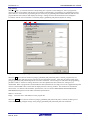
1
Cover
PG-FP5 V2.13
Flash Memory Programmer
User’s Manual
: RL78, 78K, V850, RX100, RX200, RX600 (Except RX64x), R8C, SH
All information contained in these materials, including products and product specifications,
represents information on the product at the time of publication and is subject to change by
Renesas Electronics Corporation without notice. Please review the latest information published
by Renesas Electronics Corporation through various means, including the Renesas Electronics
Corporation website (http://www.renesas.com).
Rev.2.00 Mar 2015
Notice
Notice
1.
Descriptions of circuits, software and other related information in this document are provided only to illustrate the operation of
semiconductor products and application examples. You are fully responsible for the incorporation of these circuits, software,
and information in the design of your equipment. Renesas Electronics assumes no responsibility for any losses incurred by you
or third parties arising from the use of these circuits, software, or information.
2.
Renesas Electronics has used reasonable care in preparing the information included in this document, but Renesas Electronics
does not warrant that such information is error free. Renesas Electronics assumes no liability whatsoever for any damages
incurred by you resulting from errors in or omissions from the information included herein.
3.
Renesas Electronics does not assume any liability for infringement of patents, copyrights, or other intellectual property rights of
third parties by or arising from the use of Renesas Electronics products or technical information described in this document. No
license, express, implied or otherwise, is granted hereby under any patents, copyrights or other intellectual property rights of
Renesas Electronics or others.
4.
You should not alter, modify, copy, or otherwise misappropriate any Renesas Electronics product, whether in whole or in part.
Renesas Electronics assumes no responsibility for any losses incurred by you or third parties arising from such alteration,
modification, copy or otherwise misappropriation of Renesas Electronics product.
5.
Renesas Electronics products are classified according to the following two quality grades: “Standard” and “High Quality”. The
recommended applications for each Renesas Electronics product depends on the product’s quality grade, as indicated below.
“Standard”:
Computers; office equipment; communications equipment; test and measurement equipment; audio and visual
equipment; home electronic appliances; machine tools; personal electronic equipment; and industrial robots etc.
“High Quality”: Transportation equipment (automobiles, trains, ships, etc.); traffic control systems; anti-disaster systems; anticrime systems; and safety equipment etc.
Renesas Electronics products are neither intended nor authorized for use in products or systems that may pose a direct threat to
human life or bodily injury (artificial life support devices or systems, surgical implantations etc.), or may cause serious property
damages (nuclear reactor control systems, military equipment etc.). You must check the quality grade of each Renesas
Electronics product before using it in a particular application. You may not use any Renesas Electronics product for any
application for which it is not intended. Renesas Electronics shall not be in any way liable for any damages or losses incurred
by you or third parties arising from the use of any Renesas Electronics product for which the product is not intended by Renesas
Electronics.
6.
You should use the Renesas Electronics products described in this document within the range specified by Renesas Electronics,
especially with respect to the maximum rating, operating supply voltage range, movement power voltage range, heat radiation
characteristics, installation and other product characteristics. Renesas Electronics shall have no liability for malfunctions or
damages arising out of the use of Renesas Electronics products beyond such specified ranges.
7.
Although Renesas Electronics endeavors to improve the quality and reliability of its products, semiconductor products have
specific characteristics such as the occurrence of failure at a certain rate and malfunctions under certain use conditions. Further,
Renesas Electronics products are not subject to radiation resistance design. Please be sure to implement safety measures to
guard them against the possibility of physical injury, and injury or damage caused by fire in the event of the failure of a Renesas
Electronics product, such as safety design for hardware and software including but not limited to redundancy, fire control and
malfunction prevention, appropriate treatment for aging degradation or any other appropriate measures. Because the evaluation
of microcomputer software alone is very difficult, please evaluate the safety of the final products or systems manufactured by
you.
8.
Please contact a Renesas Electronics sales office for details as to environmental matters such as the environmental compatibility
of each Renesas Electronics product. Please use Renesas Electronics products in compliance with all applicable laws and
regulations that regulate the inclusion or use of controlled substances, including without limitation, the EU RoHS Directive.
Renesas Electronics assumes no liability for damages or losses occurring as a result of your noncompliance with applicable laws
and regulations.
9.
Renesas Electronics products and technology may not be used for or incorporated into any products or systems whose
manufacture, use, or sale is prohibited under any applicable domestic or foreign laws or regulations. You should not use
Renesas Electronics products or technology described in this document for any purpose relating to military applications or use
by the military, including but not limited to the development of weapons of mass destruction. When exporting the Renesas
Electronics products or technology described in this document, you should comply with the applicable export control laws and
regulations and follow the procedures required by such laws and regulations.
10. It is the responsibility of the buyer or distributor of Renesas Electronics products, who distributes, disposes of, or otherwise
places the product with a third party, to notify such third party in advance of the contents and conditions set forth in this
document, Renesas Electronics assumes no responsibility for any losses incurred by you or third parties as a result of
unauthorized use of Renesas Electronics products.
11. This document may not be reproduced or duplicated in any form, in whole or in part, without prior written consent of Renesas
Electronics.
12. Please contact a Renesas Electronics sales office if you have any questions regarding the information contained in this document
or Renesas Electronics products, or if you have any other inquiries.
(Note 1) “Renesas Electronics” as used in this document means Renesas Electronics Corporation and also includes its majorityowned subsidiaries.
(Note 2) “Renesas Electronics product(s)” means any product developed or manufactured by or for Renesas Electronics.
(2012.4)
PG-FP5 V2.13
PREFACE
PREFACE
Thank you for purchasing the PG-FP5 flash memory programmer. The PG-FP5 is a flash memory programmer for
Renesas Electronics microcontrollers.
The manuals relevant to usage of the PG-FP5 are listed below. The manuals for your product consist of two volumes; a
common part and a part for the corresponding MCUs. Be sure to read both volumes before using the PG-FP5. You can
download the latest manuals from the Renesas Tools homepage (http://www.renesas.com/pg_fp5).
Related manuals
Document name
Document number
PG-FP5 V2.13 Flash Memory Programmer User's Manual Common
R20UT2922E
PG-FP5 V2.13 Flash Memory Programmer User's Manual RL78, 78K, V850, RX100, RX200,
RX600 (Except RX64x), R8C, SH
This manual
PG-FP5 V2.13 Flash Memory Programmer User's Manual RH850, RX700 (Include RX64x)
R20UT2924E
R20UT2923EJ0200 Rev.2.00
Mar 02, 2015
Page 3 of 80
PG-FP5 V2.13
PREFACE
Contents
PREFACE .......................................................................................................................................................... 3
Contents ..................................................................................................................................................... 4
Term replacement ....................................................................................................................................... 5
1. PROGRAMMING GUI USAGE ...................................................................................................................... 6
1.1. Introduction .......................................................................................................................................... 6
1.2. Startup of Programming GUI ............................................................................................................... 6
1.3. Menu Bar ........................................................................................................................................... 10
1.3.1. [File] menu............................................................................................................................... 10
1.3.2. [Programmer] menu ................................................................................................................ 19
1.3.3. [Device] menu ......................................................................................................................... 33
1.3.4. [Help] menu ............................................................................................................................. 63
1.4. Toolbar ............................................................................................................................................... 64
1.5. Action Log Window ............................................................................................................................ 64
1.6. Programming Parameter Window ..................................................................................................... 65
1.7. Status Bar .......................................................................................................................................... 67
1.8. Hint Bar .............................................................................................................................................. 67
2. EXAMPLE OF OPERATION USING PROGRAMMING GUI....................................................................... 68
R20UT2923EJ0200 Rev.2.00
Mar 02, 2015
Page 4 of 80
PG-FP5 V2.13
PREFACE
Term replacement
When the RX100, RX200 is used, some terms in this manual should be replaced as shown in the table below.
Term
Meaning.
Get Flash options
Access window read
Set Security
Access window program
All trademarks and registered trademarks are the property of the respective owner.
R20UT2923EJ0200 Rev.2.00
Mar 02, 2015
Page 5 of 80
PG-FP5 V2.13
PROGRAMMING GUI USAGE
1. PROGRAMMING GUI USAGE
This chapter explains functional details on windows and dialog boxes of the programming GUI.
1.1. Introduction
Make sure that the programming GUI, USB driver, and the FP5 parameter file (PR5 file) for the target device are
installed. For the installation method, refer to Common 3 SOFTWARE INSTALLATION.
1.2. Startup of Programming GUI
(1) System connection
Connect a USB cable (or serial cable) to the USB port (or serial port) on the host PC, and the other side of the cable to
the USB connector (or serial connector) on the FP5. Plug in the AC adaptor and then connect to the FP5 power supply
connector.
Serial cable
or
USB cable
AC adapter
Host PC
Outlet
FP5
Figure 1.1
System Connection
(2) FP5 startup
After the cables are connected, press the POWER button on the FP5. When the FP5 is correctly started, the POWER
LED is turned on and “Commands >” is displayed in the message display. If not, the cause may be a defect in the FP5,
so consult a Renesas Electronics sales representative or distributor.
(3) Startup of programming GUI
Click the Start menu, “All Programs”, point to “Renesas Electronics Utilities”, “Programming Tools”, and then select
“PG-FP5 Vx.xx” of “PG-FP5 Vx.xx” to start the Programming GUI. The valid communication mode is automatically
detected in the order of the USB, and then the serial interface.
Figure 1.2
Port Scanning at Startup of Programming GUI
The communication mode can also be selected by cancelling this operation by clicking the Cancel button and selecting
the [Setup host connection...] command in the [Programmer] menu.
R20UT2923EJ0200 Rev.2.00
Mar 02, 2015
Page 6 of 80
PG-FP5 V2.13
PROGRAMMING GUI USAGE
When communication is established and the programming GUI is correctly started, the main window will be opened.
Note that when the programming GUI is started for the first time, the valid programming area is cleared or once FP5
unit from a number of units has been connected, the following message will be displayed, so download the following
ESF file, PR5 file or program file. This message means that ESF file and program file in the FP5 unit and the
information stored in the programming GUI (INI file) do not match.
Figure 1.3
Message Displayed at the First Startup of Programming GUI
1.
2.
Click the OK button in the dialog box.
The following dialog box will be displayed. Click Yes or No .
3.
Clicking Yes will open a dialog box to make a new ESF file. Refer to 1.3.3 (15) (a) <3> New... button for the
steps that follow.
Clicking No will open a dialog box to select a previously created ESF file. Refer to 1.3.3 (15) (a) <3> ... button
for the steps that follow.
R20UT2923EJ0200 Rev.2.00
Mar 02, 2015
Page 7 of 80
PG-FP5 V2.13
R20UT2923EJ0200 Rev.2.00
Mar 02, 2015
PROGRAMMING GUI USAGE
Page 8 of 80
PG-FP5 V2.13
4.
PROGRAMMING GUI USAGE
Next, the device setup dialog box that is opened when [Device] menu -> [Setup...] command is executed will be
opened, so make the settings. Refer to 1.3.3 (15) [Setup] for the steps that follow.
<1> Menu bar
<4> Programmer parameter window
<2> Toolbar
<3> Action log window
<6> Hint bar
<5> Status bar
Figure 1.4
Main Window
The main window consists of the following areas.
Name
Displayed Items
Refer to:
<1>
Menu bar
Menu items executable by the programming GUI
1.3
<2>
Toolbar
Frequently used commands, as buttons
1.4
<3>
Action log window
A programming GUI action log
1.5
<4>
Programming parameter window
Programming parameter settings
1.6
<5>
Status bar
Command progress shown as a color or with a message
1.7
<6>
Hint bar
Hints for commands and toolbar
1.8
R20UT2923EJ0200 Rev.2.00
Mar 02, 2015
Page 9 of 80
PG-FP5 V2.13
PROGRAMMING GUI USAGE
1.3. Menu Bar
The menu bar displays the commands that are available for the programming GUI. Some commands may be
unavailable when the programming GUI is started for the first time, depending on the parameter file (PR5 file) selected
or FP5 Manager setting. Also, if an HCUHEX file is selected, the HCUHEX file is handled as master data, so the
[Program], [Read], [Set Security], [Set Option bytes], and [Set ID Code] commands are unavailable.
Note
During command execution, do not execute other commands or terminate the programming GUI.
1.3.1. [File] menu
The following pull-down menu appears by clicking the [File] menu.
This menu includes commands related to program file operation.
(1)
(2)
(3)
(4)
Figure 1.5
[File] Menu
(1) [Hex Editor...] command
The [Hex Editor] menu allows you to edit a program file in Intel HEX format or Motorola HEX format. When this
command is executed, a program file select dialog box is opened and the file to be edited can be specified. Note that
HCUHEX files, and DDI files cannot be loaded in this dialog box.
Figure 1.6
Program File Select Dialog Box
S-rec / Hex files (*.rec;*.s*;*.hex) or All files (*.*) may be selected from the Files of types list box.
After selecting a file to be opened, the file selected in the HEX Editor main window is loaded. At this time, whether the
file is of the Intel HEX format or Motorola HEX format is automatically recognized. When loading is finished, the
HEX Editor main window is opened.
R20UT2923EJ0200 Rev.2.00
Mar 02, 2015
Page 10 of 80
PG-FP5 V2.13
PROGRAMMING GUI USAGE
Data display area
Address display area
Figure 1.7
ASCII display area ID Tag area
HEX Editor Main Window
The displayed file contents can be modified by placing the pointer in the data display area in the HEX Editor main
window. Data input via the keyboard is accepted for all shown memory locations.
The ID Tag area is the area used with the target device supporting data flash. Only area indicating 0 or 1 can be edited
in this area. Input 0 or 1 for the ID Tag area. If 0 is input, then 00000000h will be set, and if 1 is input, FFFFFFFFh
will be used as the ID Tag. For details on data flash and ID tags, refer to the user’s manual of the target device.
The HEX Editor only accepts hexadecimal data, i.e., numbers 0 to 9 and letters A to F. All other data will be rejected.
The ASCII representation, if any, is shown in the ASCII display area. This area is for reference only, so no data can be
input.
Use the scroll bar to move another address range into the visible area of the HEX Editor.
The following keys can be input using the keyboard.
Table 1.1 Key Functions That Can Be Input in HEX Editor Window
Key
0-9, A-F
Function
Data input (data display area)
Move cursor in right direction
Move cursor in left direction
Move cursor in up direction
Move cursor in down direction
Tab Move cursor to next input field (address + 1)
If any changes have been made to the file, [Save] and [Save As] in the [File] menu in the HEX Editor main window
become available for saving the modified data.
R20UT2923EJ0200 Rev.2.00
Mar 02, 2015
Page 11 of 80
PG-FP5 V2.13
PROGRAMMING GUI USAGE
(a) When a 78K product or V850 and RL78 family product without data flash memory is selected
(b) When a V850 or RL78 family product with data flash memory is selected
R20UT2923EJ0200 Rev.2.00
Mar 02, 2015
Page 12 of 80
PG-FP5 V2.13
PROGRAMMING GUI USAGE
(c) When the RX family, R8C family, or SuperH family is selected
Figure 1.8
[Save As] Dialog Box of HEX Editor
Besides the file name and folder location, a start address and an end address for the new file can be selected in the [Save
As] dialog box. The original start address and end address are displayed by default. Select the file radio button for the
format in which to save the data. Select the same format as that of the loaded file. Use of the saved file with other tool
products is not supported.
Note
In a microcontroller that supports ID Tags of data flash, for the saved program file contents of the data flash
area, refer to Common APPENDIX B SUPPLEMENTARY INFORMATION Figure B.1 Relationship Between
HEX Editor and Saved Program File.
Mapping of the data flash memory may differ between normal operation and flash memory programming mode.
Refer to the user’s manual of the MCU for more information on mapping when the flash memory programming
mode is selected.
R20UT2923EJ0200 Rev.2.00
Mar 02, 2015
Page 13 of 80
PG-FP5 V2.13
PROGRAMMING GUI USAGE
(2) [Upload from FP5...] command
The [Upload from FP5...] command is used to upload the program file, PR5 file and ESF file saved in a valid
programming area.
<1>
<2>
<3>
<4>
(a) When a 78K product or V850 and RL78 family product without data flash memory is selected
<1>
<2>
<3>
<4>
(b) When a V850 or RL78 family product with data flash memory is selected
R20UT2923EJ0200 Rev.2.00
Mar 02, 2015
Page 14 of 80
PG-FP5 V2.13
PROGRAMMING GUI USAGE
<1>
<2>
<3>
<4>
(c) When the RX family, R8C family, or SuperH family is selected
Figure 1.9
[Upload from FP5...] Dialog Box in the HEX Editor
<1> [Upload program file from FP5] button
The storage location and file name of the program file are specified in the HEX file: box. In order to change the file
location or name, click the Save as button and make the changes.
<2> [Upload Parameter/Setting files from FP5] button
The Parameter file: box specifies the storage location of the PR5 file. The Setting file: box specifies the ESF file
storage location and file name. In order to change the file locations, click the Save as button and make the changes.
The parameter file names cannot be changed.
<3> Address range selection area
This area is enabled with the [Upload program file from FP5] button clicked. Specify the address range of the program
file that is to be saved. When a V850 and RL78 family product with data flash memory is selected, [Code flash:] and
[Data flash:] are displayed. For the RX family, R8C family, and SuperH family, [User mat], [Data mat], and [User boot]
are displayed.
<4> Option area
When the [Show data] check box is checked, the action log window will be displayed when the upload is executed.
Pressing the OK button will start the upload with the selected settings.
Pressing the Cancel button will close the dialog box without executing the upload.
R20UT2923EJ0200 Rev.2.00
Mar 02, 2015
Page 15 of 80
PG-FP5 V2.13
PROGRAMMING GUI USAGE
(3) [Checksum] command
The [Checksum] command calculates the checksum of the selected program file downloaded to FP5 and displays the
result. When this command is executed, the Checksum dialog box appears. Select the optional calculation method and
the target address range, and click the OK button. The result will then be displayed in the [File Checksum] area in the
action log window and programmer parameter window. This command can be executed after the [Setup] command is
executed. If the [Setup] command is executed again after the [Checksum] command is executed, the result displayed in
the [File Checksum] area in the programmer parameter window will be cleared.
<1>
<1>
<2>
<2>
<3>
<3>
(a) When a 78K product or V850 and RL78 family product
without data flash memory is selected
(b) When a V850 or RL78 family product with data flash
memory is selected
<1>
<2>
<3>
(c) When the RX family, R8C family, or SuperH family is selected
Figure 1.10 Checksum Dialog Box
<1> Programming area
The valid programming area is displayed.
<2> Checksum calculation mode selection
Select the mode for calculating checksum of the selected program file. Selected calculation modes differ with the MCU.
R20UT2923EJ0200 Rev.2.00
Mar 02, 2015
Page 16 of 80
PG-FP5 V2.13
Table 1.2
PROGRAMMING GUI USAGE
Checksum calculation
Checksum calculation
Correspondence microcontroller
Arithmetic
checksum (16bit)
16-bit arithmetic
(subtraction)
78K and V850 products, and RL78 family products that support the
Checksum command
Arithmetic
checksum
32-bit arithmetic
(addition)
RX, R8C, and SuperH families
CRC sum (16bit)
16-bit CRC
RL78 family products that support the CRC check command
CRC sum (32bit)
32-bit CRC
78K and V850 products, RL78 family products that support the Checksum
command, RX, R8C, and SuperH families
Note
With the 16-bit arithmetic (subtraction) mode, the lower 4 digits of the result from which a value is subtracted
from 00h in 1-byte units are displayed.
With the 32-bit arithmetic (addition) mode, the lower 8 digits of the result to which a value is added from 00h in 1byte units are displayed.
With 16-bit mode, the 4-digit result of CRC16 function calculation is displayed. For details on arithmetic
specifications, refer to Common APPENDIX B SUPPLEMENTARY INFORMATION Figure B.5 16-bit CRC
Calculation Specifications.
With 32-bit mode, the 8-digit result of CRC32 function calculation is displayed. For details on arithmetic
specifications, refer to Common APPENDIX B SUPPLEMENTARY INFORMATION Figure B.2 32-bit CRC
Calculation Specifications.
<3> Address range selection
Select the range for calculating checksum of the selected program file. If there is no program file data in the specified
range, the specified range is filled with FFh for calculation. When a V850 or RL78 family product with data flash
memory is selected, [Code flash:] and [Data flash:] are displayed. When the RX family, R8C family, or SuperH family
is selected, [User mat], [Data mat], and [User boot] are displayed.
Device Area: From the start to end addresses of the device, which are contained in the selected PR5 file
User Defined: Any range can be specified by inputting the addresses to the [Start Address] and [End Address] text
boxes.
Clicking the OK button displays the calculation result in the [File Checksum] area in the action log window and
programmer parameter window.
Clicking the Cancel button closes the dialog box without saving the settings made in the Checksum dialog box.
Note
Note
When the valid programming area is changed or a program file is downloaded, the checksum result will be
cleared.
When the RX family, or SuperH family is selected, when ROM size is less than 8Kx2^n byte, a space area is
complemented with FFh to an 8Kx2^n byte, and the range of an 8Kx2^n byte is calculated.
Ex.1) When ROM size is 384 K bytes, a space area is complemented with FFh to a 512K byte, and the range of
a 512K byte is calculated.
Ex.2) When ROM size is 256 K bytes, a space area is complemented with FFh to 256 K bytes, and 256 K bytes
of range is calculated.
R20UT2923EJ0200 Rev.2.00
Mar 02, 2015
Page 17 of 80
PG-FP5 V2.13
PROGRAMMING GUI USAGE
(a) When a 78K product or V850 and RL78 family product without data flash memory is selected
(b) When a V850 or RL78 family product with data flash memory is selected
R20UT2923EJ0200 Rev.2.00
Mar 02, 2015
Page 18 of 80
PG-FP5 V2.13
PROGRAMMING GUI USAGE
(c) When RX Family, R8C Family or SuperH Family Is Selected
Figure 1.11 Checksum Result
(4) [Quit] command
The [Quit] command terminates the programming GUI. The programming GUI can also be terminated by clicking the
× button on the right end of the title bar in the main window. When the programming GUI is terminated, various
settings are saved in the INI file (FP5.ini), and these settings are loaded when the programming GUI is started the next
time.
1.3.2. [Programmer] menu
Clicking the [Programmer] menu displays the following pull-down menu.
This menu includes commands related to FP5 settings.
(1)
(2)
(3)
(4)
(5)
(6)
(7)
(8)
(9)
Figure 1.12 [Programmer] Menu
R20UT2923EJ0200 Rev.2.00
Mar 02, 2015
Page 19 of 80
PG-FP5 V2.13
PROGRAMMING GUI USAGE
(1) [Setup host connection] command
Running the [Setup host connection] command opens the [Host Connection] dialog box. The channel for
communication between the FP5 and the host PC can be selected and configured in this dialog box.
Figure 1.13 [Host Connection] Dialog Box
“USB” can be selected as the communication channel if the USB interface is supported in the PC used.
When selecting “Serial”, select the COM port and baud rate from the drop-down list boxes. COM ports that are
recognized by the host PC are displayed in the Port list. Up to 256 ports can be recognized.
When the OK button is clicked, software tries to establish a connection between the FP5 and the host PC using the
selected communication channels.
Clicking the Cancel button closes the window without making any changes.
(2) [Logging] command
The [Logging] command saves information displayed in the action log window in the log file. When this command is
executed, the log file save dialog box appears. Move to an arbitrary folder, select the log file in the [File name] dropdown list, and click the Save button; the log file will then be saved. The [Logging] command on the menu bar will be
checked. The check mark will be cleared by clicking the [Logging] command again and saving of the log file will be
stopped. Enabling/disabling the [Logging] command is added to the time stamp. For a log file example, refer to
Common APPENDIX B SUPPLEMENTARY INFORMATION Figure B.3 Log File Example.
Note
The log file that was saved the last time is displayed in the log file save dialog box.
Figure 1.14 Log File Save Dialog Box
Clicking the Save button saves the specified log file.
Clicking the Cancel button closes the dialog box without saving the log file.
R20UT2923EJ0200 Rev.2.00
Mar 02, 2015
Page 20 of 80
PG-FP5 V2.13
PROGRAMMING GUI USAGE
(3) [Select Programming area] command
The FP5 has a 16 MB flash memory area for saving program files. This memory area can be used as two programming
areas of 10 MB and 6 MB (Area 0 to Area 1), four 4 MB programming areas (Area 0 to Area 3) or eight independent 2
MB programming areas (Area 0 to Area 7). Program files can be downloaded to each programming area, and which file,
PR5 or ESF, is to be saved is selectable in programming area units. That is, files can be individually downloaded in
each programming area, and the area used can also be selected individually.
This command is used to select a valid programming area from the FP5’s programming areas x. When this command is
executed, the programming area select dialog box is opened, and the desired programming area can be selected. The
number of programming areas that can be selected with this command is the value defined in the [Programming Area
Setting] area on the [Target] tab of the Device Setup dialog box, which is opened by the [Setup...] command in the
[Device] menu.
Figure 1.15 Programming Area Select Dialog Box
The currently selected programming area is displayed in the programming area selection dialog box. To change the area,
select the relevant number from the list box and click the OK button. To check the contents set to each area or to
change the division factor, see the [Target] tab of the Device Setup dialog box.
Clicking the OK button selects the programming area selected in the programming area select dialog box.
Clicking the Cancel button closes the dialog box without changing the programming area.
(4) [Buzzer] command
The [Buzzer] command is used to enable or disable the setting to output the buzzer sound from the FP5 main unit.
When this command is executed, the [Buzzer] command on the menu bar is checked and becomes valid. When this
command is executed again, the check mark is cleared and the command becomes invalid. The FP5 makes a doublebeep sound when the Autoprocedure(E.P.) command is completed normally, or makes a buzzer sound when the
command is completed abnormally.
(5) [Reset] command
When the [Reset] command is executed, a software reset can be applied to the FP5. After reset, the current versions of
the firmware, FPGA, the FP5 serial number, and mode will be displayed in the action log window.
(6) [Self-Test] command
The [Self-Test] command executes the FP5 self-testing program. The following three items are subject to self-testing.
The self-testing program does not affect the PR5 files, ESF files and program files saved in the FP5.
<1> FPGA test
<2> Power generation block test
<3> Target / remote interface I/O test
Since execution of the [Self-Test] command involves I/O testing, a message that prompts the user to disconnect
hardware connected the target connector or remote connector is displayed. Remove hardware (including target system
and program adaptor), connected to the target connector or remote connector, if any. Make sure that no hardware is
connected and click the OK button; self-testing will then be executed.
If the Cancel button is clicked, self-testing will not be executed.
R20UT2923EJ0200 Rev.2.00
Mar 02, 2015
Page 21 of 80
PG-FP5 V2.13
PROGRAMMING GUI USAGE
Figure 1.16 Confirmation Before Starting Self-Testing
Self-testing takes about three seconds, and the result will be displayed in the action log window and a result dialog box.
If the message “Selftest FAILED.” is displayed, the cause may be a defect in the FP5, so consult a Renesas Electronics
sales representative or distributor.
>selftest
***** CAUTION *****
Remove any plugs from Target- and Remote-Connector before starting.
Any hardware attached to those connectors may be damaged by this test !
***** CAUTION *****
Target- and Remote-connector unplugged ?
If yes, press 's' to start the test: s
FPGA Test: PASS
Power Supply Test: PASS
Target- and Remote-Interface Test: PASS
Selftest PASSED.
>
Figure 1.17 Result When Self-Testing Program Has Been Completed Normally <Action Log Window>
Figure 1.18 Result When Self-Testing Program Has Been Completed Normally <Result Dialog Box>
R20UT2923EJ0200 Rev.2.00
Mar 02, 2015
Page 22 of 80
PG-FP5 V2.13
PROGRAMMING GUI USAGE
>selftest
***** CAUTION *****
Remove any plugs from Target- and Remote-Connector before starting.
Any hardware attached to those connectors may be damaged by this test !
***** CAUTION *****
Target- and Remote-connector unplugged ?
If yes, press 's' to start the test: s
FPGA Test: PASS
Power Supply Test: PASS
Target- and Remote-Interface Test: FAIL
Selftest FAILED.
>
Figure 1.19 Example of Result When Self-Testing Program Has Been Completed Abnormally <Action Log
Window>
Figure 1.20 Example of Result When Self-Testing Program Has Been Completed Abnormally <Result Dialog
Box>
(7) [Update Firmware] command
The [Update Firmware] command updates the firmware. Refer to Common 3.4 Updating Programming GUI, Firmware
and FPGA and download the relevant update file before starting update.
Executing of this command displays the following dialog box.
Figure 1.21 [Update Firmware] Dialog Box
To continue the firmware update, click the OK button.
Clicking the Cancel button cancels the firmware update.
Clicking the OK button opens the [Open firmware file] dialog box.
R20UT2923EJ0200 Rev.2.00
Mar 02, 2015
Page 23 of 80
PG-FP5 V2.13
PROGRAMMING GUI USAGE
Figure 1.22 [Open firmware file] Dialog Box
Select the firmware file “fp5_fw_vxxx.rec” and then click the Open button.
Note
1. Do not use FP5 firmware other than the one posted on the website; otherwise, a defect may occur.
2. When a firmware of FP5 updates from V2.00 to V1.xx, a serial number of FP5 is erased.
And, FP5 can't operate in USB1.1. In addition, the other functions don't have any problem.
When FP5 revives, consult a Renesas Electronics sales representative or distributor.
Some commands are sent to the FP5 and the update progress status is displayed in the action log window. The message
“Firmware Update succeeds”, which indicates normal completion of firmware update, and “Restarting FP5...”, which is
equivalent to [RESET] command processing, is automatically performed. The new version can then be checked as
“Firmware Version Vx.xx”. The update takes about 10 seconds.
R20UT2923EJ0200 Rev.2.00
Mar 02, 2015
Page 24 of 80
PG-FP5 V2.13
PROGRAMMING GUI USAGE
Figure 1.23 Action Log Window When Firmware Update Is Finished
Note
Depending on the changes made, the following dialog box will be displayed. In this case, the information stored
in the FP5 (PR5 file, ESF file, program file) will have been deleted, so please download those files again. (Refer
to 1.2 Startup of Programming GUI.)
(8) [Update FPGA] command
The [Update FPGA] command updates the FPGA. Refer to Common 3.4 Updating Programming GUI, Firmware and
FPGA and download the relevant update file before starting update.
Executing of this command displays the following dialog box.
R20UT2923EJ0200 Rev.2.00
Mar 02, 2015
Page 25 of 80
PG-FP5 V2.13
PROGRAMMING GUI USAGE
Figure 1.24 [Update FPGA] Dialog Box
To continue the FPGA update, click the OK button.
Clicking the Cancel button cancels the FPGA update.
Clicking the OK button opens the [Open FPGA file] dialog box.
Figure 1.25 [Open FPGA file] Dialog Box
Select the FPGA file “fp5_fpga_vx.rec” and then click the Open button.
Note
Do not use FP5 FPGA other than the one posted on the website; otherwise, a defect may occur.
Some commands are sent to the FP5 and the update progress status is displayed in the action log window. The message
“FPBGA Upload succeeded.”, which indicates normal completion of firmware update, and “FP5 Power will be
switched OFF now.....”, which is equivalent to processing when the POWER button is turned off, is automatically
executed. The update takes about 30 seconds.
R20UT2923EJ0200 Rev.2.00
Mar 02, 2015
Page 26 of 80
PG-FP5 V2.13
PROGRAMMING GUI USAGE
Figure 1.26 Action Log Window When FPGA Update Is Finished
Click the OK button in the error message dialog box and then press the POWER button on the FP5 to turn on power.
Execution of the [Setup host connection...] command opens the [Host Connection] dialog box. Select the
communication mode used and then click the OK button.
Figure 1.27 [Setup host connection] Command
R20UT2923EJ0200 Rev.2.00
Mar 02, 2015
Page 27 of 80
PG-FP5 V2.13
PROGRAMMING GUI USAGE
Figure 1.28 [Host Connection] Dialog Box
The main window is opened. “Board H/W V1, FPGA Vx” is displayed in the action log window; thus, the version can
be checked.
Figure 1.29 Version Confirmation After FPGA Update Is Finished
(9) [FP5 Manager] command
The [FP5 Manager] command sets the FP5 management functions. These functions include the following: The
password function, the upload prohibit function, the device setup prohibit function, the bank mode enable function, the
simple mode enable function, the checksum comparison function, the program file size monitoring function, unique
code embedding function, and the reset terminal property switching function.
When the [FP5 Manager] command is executed, the following dialog will be opened.
R20UT2923EJ0200 Rev.2.00
Mar 02, 2015
Page 28 of 80
PG-FP5 V2.13
PROGRAMMING GUI USAGE
If a password is not registered, the dialog box in Fig. 1.30 will open.
If a password is registered, the dialog box in Fig. 1.32 will open.
Figure 1.30 Welcome to FP5 Manager Dialog Box
Clicking Yes will open the following dialog box.
Clicking No will close the dialog box.
Figure 1.31 Password setting Dialog Box
In order to register a password, input a password into the [PASSWORD] box and [Confirm PASSWORD] box, and then
click OK .
The password must be made up of up to eight alphanumeric characters. (Differences in upper and lower case are not
recognized.)
Clicking Cancel will close the dialog box.
Figure 1.32 Login to FP5 Manager Dialog Box
Input the password into the [PASSWORD] box, and then click OK .
If the password is correct the dialog box in Figure 1.34 will open. If the password is wrong, then the dialog box in
Figure 1-33 will open.
Clicking Cancel will close the dialog box.
R20UT2923EJ0200 Rev.2.00
Mar 02, 2015
Page 29 of 80
PG-FP5 V2.13
PROGRAMMING GUI USAGE
Figure 1.33 FP5 Dialog Box
Clicking Yes will open the dialog box to input the password again (Figure 1.32).
Clicking No will initialize the FP5 to its default settings. When initialized, the following stored information will be
deleted or reset to their defaults:
• Password
•
FP5 Manager setting
•
PR5 file
•
ESF file
•
Program file
Clicking Cancel will close the dialog box.
Figure 1.34 FP5 Manager Dialog Box
After making any changes to the settings and clicking OK, the dialog box will close and the settings will be enabled.
Clicking Cancel will close the dialog box and discard the changes. The FP5 Manager settings are described below.
•
Displaying Mode Contents
The mode contents that indicate the FP5 state is displayed in the [Programmer] area of the programming parameter
window.
• Standard mode unsecured
The FP5 Manager has not been set.
•
Standard mode secured
The FP5 Manager has been set. However, the bank mode or the simple mode have not been set.
•
Bank mode secured
The FP5 Manager and bank mode have been set.
R20UT2923EJ0200 Rev.2.00
Mar 02, 2015
Page 30 of 80
PG-FP5 V2.13
•
PROGRAMMING GUI USAGE
Simple mode secured
The FP5 Manager and simple mode have been set.
•
FP5 Manager Dialog Settings (Refer to Figure 1.34)
[Disable Upload] check box
This sets enabling or disabling of the upload function used to upload data (program file, PR5 file, ESF file) from the
valid programming area of FP5 to the host PC. Checking the box will disable and unchecking it will enable the
function. When this function is disabled, the [File] menu -> [Upload from FP5...] command, and the hex, srec, and
upset of the communications command are disabled. The default is not to have this box checked.
[Disable Device Setup] check box
Enables or disables the [Setup] command in the [Device] menu. It is disabled when checked, and enabled when not
checked. When it is disabled, the [Setup] command in the [Device] menu, as well as the downprm, downset, and lod
communication commands become invalid.
[Enable Bank mode] check box
Sets the normal mode or bank mode for the mode of the remote connector. Checking this box will set the bank mode,
and not checking it will set the normal mode. If checked, [Enable Simple mode] cannot be checked. When in the bank
mode, the programming area can be selected through the remote connector. With respect to detailed functions, refer to
Common 5 USAGE THE REMOTE CONNECTOR. The default is not to have this box checked.
[Enable Simple mode] check box
Sets the normal mode or the simple mode. Checking this box will set the simple mode, and not checking it will set the
normal mode. If checked, [Enable Bank mode] cannot be checked. When in the simple mode, the functions of the FP5
control buttons and message display will change. When
the NEXT button is clicked, the programming area will be switched. Clicking the ENTER button
or START button will execute the Autoprocedure(E.P.) command. The message display will display (1) the
programming area number, (2) the program file name, and (3) the checksum and (4) command name. Immediately after
the program file is downloaded, the checksum will show H:xxxxxxxx. At this time, the program file will be checked
using 32-bit CRC calculations from the start to the end address. After this, executing [File] menu -> [Checksum]
command will display F:xxxxxxxx. The default is not to have this box checked.
(1)
(3)
(2)
0:sample.hex
H:AFE33BC0 E.P.>
(4)
Figure 1.35 Example of Message Display
[Checksum comparison] check box
When [Device] menu -> [Checksum] command is executed and the checksum of the target device is displayed, the
checksum of the program file stored in FP5 will be referenced and the results displayed. Checking this box will crossreference the checksum, and not checking it will not. The default is not to have this box checked.
>Sum
Checksum: 0x623E
Checksum compare: PASS
Checksum operation: finished.
Figure 1.36 Example of Action Log Window
[Program file size monitor function] check box
Halts execution of programming commands if the program file size exceeds the programmable range. If this check box
is checked and the address range of the downloaded program file exceeds the address range specified in the [Operation
R20UT2923EJ0200 Rev.2.00
Mar 02, 2015
Page 31 of 80
PG-FP5 V2.13
PROGRAMMING GUI USAGE
Mode] area on the [Standard] tab of the Device Setup dialog box, executing a [Program], [Verify], or
[Autoprocedure(E.P.)] command will cause the error message “ERROR (E302): Hex file exceeds target device flash
range.” to appear in the Action Log window and execution of the command will halt. If this check box is not checked,
the warning message “WARNING: HEX file exceeds target device flash range.” will appear in the Action Log window,
but execution of the command will continue. The default is not to have this box checked.
[Enable Serial Number mode] check box
Serial Number mode (Unique code embedding function) is for embedding a unique code in the specified area of a
program file that has been read. The code is embedded by issuing the serno command with the code and area specified.
Placing a check mark in this box enables the unique code embedding function. For more information on the serno
command, refer to Common 6.4.18 serno command.
[Reset option of Run after Disconnect]
When the [Run after Disconnect] function in the [Command options] area of the Device setup dialog [Advanced] tab is
¯¯¯¯¯¯ signal after the write command is completed can be set to Pull-up or Hi-Z. The
enabled, the properties of the RESET
default is Hi-Z.
[Change the PASSWORD] button
Clicking the [Change the PASSWORD] button will open the following dialog box.
Figure 1.37 Password setting Dialog Box
This dialog box allows the user to change the registered password.
Input the current password into the [OLD PASSWORD] box, input the new password into the [NEW PASSWORD] box
and [Confirm PASSWORD] box, and then click OK. When Cancel is clicked, the dialog box will be closed and the
password will not be changed.
[INIT] button
Resets the FP5 to its default settings. Initializing the FP5 will reset or delete the following stored information.
• Password
•
FP5 Manager setting
•
PR5 file
•
ESF file
•
Program file
R20UT2923EJ0200 Rev.2.00
Mar 02, 2015
Page 32 of 80
PG-FP5 V2.13
PROGRAMMING GUI USAGE
1.3.3. [Device] menu
The following pull-down menu appears by clicking the [Device] menu.
This menu includes commands mainly related to programming to the target device, such as erase, write and verify.
Figure 1.38 [Device] Menu
(1) [Blank check] command
The [Blank Check] command performs blank check for the flash memory in the target device. The target area can be
set in the [Operation Mode] area on the [Standard] tab in the Device Setup dialog box. If the flash memory has not yet
been written, “PASS” is displayed. If the flash memory has already been written, “ERROR(E051):Not Blank” is
displayed. If this error is displayed, erase the entire flash memory before starting programming.
(2) [Erase] command
The [Erase] command erases the flash memory in the target device. The target area can be set in the [Operation Mode]
area on the [Standard] tab in the Device Setup dialog box. If this command is executed with [Chip] selected, security
command options are initialized at the same time. While erasing the flash memory is in progress, the progress status is
displayed in the action log window. When execution of this command is completed, the result of command execution in
the target device is displayed. Whether to perform the [Blank Check] command before executing this command
depends on the [Blank check before Erase] check box setting in the [Command options] area on the [Advanced] tab in
the Device Setup dialog box. If this command is executed for the target device that has already been erased with the
[Blank check before Erase] check box selected, “OK, Erase skipped.” is displayed and erasure is not performed.
(3) [Program] command
The [Program] command transmits the memory contents (program files) in the FP5 valid programming area to the target
device and writes the programs to the flash memory. The target area can be set in the [Operation Mode] area on the
[Standard] tab in the Device Setup dialog box. The progress status of this command is displayed as a percentage in the
action log window. When execution of this command is completed, the programming GUI displays the result of
command execution in the target device. Command options after execution of this command depend on the settings of
the [Verify after Program], [Security after Program] and [Checksum after Program] check boxes in the [Command
options] area on the [Advanced] tab in the Device Setup dialog box. For details on these check boxes, refer to 1.3.3
(15) (c) <2> [Command options] area.
R20UT2923EJ0200 Rev.2.00
Mar 02, 2015
Page 33 of 80
PG-FP5 V2.13
PROGRAMMING GUI USAGE
(4) [Verify] command
For the 78K, V850, and RL78 family, the [Verify] command transmits the memory contents (program files) in the FP5
valid programming area to the target device, verifies the data written to the flash memory in the target device, and
receives the result. For the RX family, R8C family, and SuperH family, it reads data from the microcontroller, and
compares it with the memory content (program file) in the effective programming area of the FP5. The target area can
be set in the [Operation Mode] area on the [Standard] tab in the Device Setup dialog box. The progress status of this
command is displayed as a percentage in the action log window. When execution of this command is completed, the
programming GUI displays the result of command execution in the target device.
(5) [Read] command
The [Read] command loads data on the flash memory in the target device and saves it as a file. The target range of the
flash memory is specified in the [Operation Mode] area on the [Standard] tab of the Device Setup dialog box. When the
[View] command is executed following this command, 4 KB read data is displayed in the log window each time the
ENTER key is pressed. When the [Write Intel HEX file] or [Write Motorola SREC file] command is executed
following this command, the read data can be saved in the Intel HEX format or Motorola HEX format. Use of the
saved file with other tool products is not supported.
Note
The folder in which program data was saved the last time is displayed in the program data save dialog box.
Figure 1.39 Program Data Saved Dialog Box <When Write Intel HEX file Command Is Executed>
R20UT2923EJ0200 Rev.2.00
Mar 02, 2015
Page 34 of 80
PG-FP5 V2.13
PROGRAMMING GUI USAGE
Figure 1.40 Program Data Save Dialog Box <When Write Motorola SREC file Command Is Executed>
Clicking the Open button saves the program data into a file and closes the dialog box.
Clicking the Cancel button closes the program data save dialog box without saving the program data into a file.
(6) [Set Security] command
The [Set Security] command sets the security functions for the target device. When this command is executed, the
settings made in the [Set Security command options] area on the [Advanced] tab in the Device Setup dialog box will be
reflected in the target device. For details on the security functions, refer to 1.3.3 (15) (c) <4> [Set Security command
options] area.
(7) [Checksum] command
For the 78K, V850, RL78 family, RX family, and SuperH family, the [Checksum] command reads the checksum
calculated in the target device and displays it in the action log window. When using a 78K0S/Kx1+ microcontroller or
the µPD78F9334, this command also displays the checksum of the program file and compares both. For the R8C
family, it reads the content of the flash memory of the target device, and displays the checksum calculated in the FP5 on
the action log window.
Note
The checksum read by this command differs from the one displayed in the [File checksum] area in the
programmer parameter window. For details on the [File checksum] area, refer to 1.3.1 (3) [Checksum]
command.
The checksum is calculated as follows. Note that this is the result when the [Enable Checksum Compare Function]
check box of the FP5 manager dialog box is not selected.
R20UT2923EJ0200 Rev.2.00
Mar 02, 2015
Page 35 of 80
PG-FP5 V2.13
PROGRAMMING GUI USAGE
<When using 78K (other than 78K0S/Kx1+, UPD78F9334), V850E1, V850ES, RL78 family>
Method: Subtraction (16-bit arithmetic)
Range: Area set in the [Operation Mode] area on the [Standard] tab in the Device Setup dialog box
>sum
Code flash: 0x8FCD
Data flash: 0x1000
Total:
0x9FCD
PASS
Checksum operation finished.
>
Figure 1.41 Action Log Window After [Checksum] Command Execution <When using 78K (Other than
78K0S/Kx1+, UPD78F9334), V850E1, V850ES, RL78 family>
Note
With the 16-bit arithmetic (subtraction) mode, the lower 4 digits of the result from which a value is subtracted
from 00h in 1-byte units are displayed.
<When using a 78K0S/Kx1+ microcontroller or UPD78F9334>
Method: Division (original)
Range: Area set in the [Operation Mode] area on the [Standard] tab in the Device Setup dialog box
>sum
Device Checksum: 0x1842
FP5 Checksum:
0x1842
Checksum compare: PASS
Checksum operation finished.
>
Figure 1.42 Action Log Window After [Checksum] Command Execution (When using 78K0S/Kx1+
microcontroller or UPD78F9334)
Note
For details on the arithmetic specifications, refer to Common APPENDIX B SUPPLEMENTARY INFORMATION
Figure B.4 Division (Original) Calculation Specifications.
<V850E2>
Method: 32-bit CRC
Range: Area specified in the [Operation Mode] area on the [Standard] tab in the Device Setup dialog box
>sum
Code flash: 0x370A7BE5
Data flash: 0xBFD1B03F
Total: 0xF6DC2C24
PASS
Checksum operation finished.
>
Figure 1.43 Action Log Window After [Checksum] Command Execution (V850E2)
Note
32-bit CRC displays the 8-digit result of CRC32 function operation. For the calculation specifications, refer to
Common APPENDIX B SUPPLEMENTARY INFORMATION Figure B.2 32-bit CRC Calculation Specifications.
R20UT2923EJ0200 Rev.2.00
Mar 02, 2015
Page 36 of 80
PG-FP5 V2.13
PROGRAMMING GUI USAGE
<RX family, R8C family, SuperH family>
Method: 32-bit arithmetic (addition) mode
Range: Result of calculating all the areas (user mat, data mat, user boot) selected in the [Operation Mode] area on the
[Standard] tab of the Device Setup dialog box
>sum
User mat:
0x03FC0000
Data mat:
0x00444588
User Boot mat: 0x003FC000
Total:
0x04800588
PASS
Checksum operation finished.
>
Figure 1.44 Action Log Window After [Checksum] Command Execution (RX Family, R8C Family, SuperH
Family)
Note
With the 32-bit arithmetic (addition) mode, the lower 8 digits of the result to which a value is added from 00h in 1byte units are displayed.
(8) [Autoprocedure(E.P.)] command
The [Autoprocedure(E.P.)] command executes the [Erase] and [Program] commands in succession. For more
information, refer to the sections on the [Erase] and [Program] commands.
>ep
Blank check Chip:
PASS, Erase skipped.
Program Chip:
10%
20%
30%
40%
50%
60%
70%
80%
90%
100%
PASS
Erase, Program operation finished.
>
Figure 1.45 Action Log Window After [Autoprocedure(E.P.)] Command Execution
(9) [Set Option bytes] command
The [Set Option bytes] command specifies the settings for the target device's option byte. When this command is
executed, the settings specified in the [Option byte setting] area on the [Advanced] tab of the Device Setup dialog box
are applied to the target device. For details of the option byte settings, see 1.3.3 (15) (c) <9> [Option bytes setting]
area.
(10) [Set ID Code] command
The [Set ID Code] command specifies the settings for the target device's option byte. When this command is executed,
the settings specified in the [OCD ID setting] area on the [Advanced] tab of the Device Setup dialog box are applied to
the target device. For details of the OCD security ID settings, see 1.3.3 (15) (c) <8> [OCD security ID setting] area.
(11) [Set Lock bits] command
The [Set Lock bits] command specifies the lock bits of the target device. When this command is executed, the settings
specified in the [Set Lock bits] area on the [Advanced] tab in the Device Setup dialog box are reflected to the target
device. For detais about lock bit settings, refer to 1.3.3 (15) (c) <11> [Lock bit setting] area.
R20UT2923EJ0200 Rev.2.00
Mar 02, 2015
Page 37 of 80
PG-FP5 V2.13
PROGRAMMING GUI USAGE
(12) [Connect] command
Executes the con command or dcon command. When the con command is executed a check will be added and when the
dcon command is executed the check will be removed. When “autocon off” or “autocon on” is executed with the
autocon command, the [connect] command is enabled or disabled. Refer to Common 6 USAGE COMMUNICATION
COMMANDSfor details about the functions.
(13) [Signature read] command
The [Signature read] command reads target device product information.
The read result is displayed in the action log window.
(14) [Get Flash options] command
The [Get Flash options] command reads the settings for the flash options for the target device and displays the result in
the [Flash options] area on the [Advanced] tab in the Device Setup dialog box. When execution of this command is
enabled, execute this command before the [Set Security] command, [Set Option bytes] command, or [Set ID Code]
command; the settings for the security functions or the boot area can thus be checked. For details on the flash option
settings, refer to 1.3.3 (15) (c) <3> [Flash options] area.
Note
When loading an HCUHEX file, the HCUHEX file is handled as master data, so even though the flash option
settings specified for the device can be checked by executing the [Get Flash Options] command, these settings
cannot be applied to the device. The OK button in the Device Setup dialog box is therefore unavailable. In this
case, click the Cancel button and close the Device Setup dialog box. Note that the OK button becomes
available if the HCUHEX file is changed to a HEX file in the [Object HEX file] area. After changing the file, the
HCUHEX file information remains unchanged in the [Command Options] and [Flash options] areas.
Figure 1.46 [Get Flash options] Command
R20UT2923EJ0200 Rev.2.00
Mar 02, 2015
Page 38 of 80
PG-FP5 V2.13
PROGRAMMING GUI USAGE
(15) [Setup]
When the [Setup...] is executed, the Device Setup dialog box is opened. In this dialog box, select a program file,
perform settings in accordance with the user environment for flash memory programming, set command option and
option data etc.. Each time the programming GUI is started, the programming GUI loads the PR5 file, ESF file and
program file that were used last and displays the settings. Settings for the items not dimmed can be changed in
accordance with the user environment. Switch the [Target], [Standard] and [Advanced] tabs for setting.
(a)
(b)
(c)
Figure 1.47 Device Setup Dialog Box
When the OK button (button common to [Target], [Standard] and [Advanced] tabs) is clicked, program areas are
cleared and PR5 files, ESF files and program files are downloaded for the FP5. After that, the settings made on the
[Target], [Standard] and [Advanced] tabs are saved into an ESF file. These settings are reflected to the programming
parameter window. If there are settings which have not been updated, the files related to the settings are not
downloaded. When a program file is downloaded, the date and checksum (An empty area will be supplemented by FFh
when it is downloaded to FP5.) of that file are displayed in the action log window. The checksum is calculated as
shown below. For details of the arithmetic specifications, refer to Common APPENDIX B SUPPLEMENTARY
INFORMATION Figure B.2 32-bit CRC Calculation Specifications.
Method: 32-bit CRC
Range: From the start to end addresses in the program file
When the Cancel button (button common to [Target], [Standard] and [Advanced] tabs) is clicked, the dialog box is
closed without saving changed settings on the [Target], [Standard] and [Advanced] tabs into an ESF file.
R20UT2923EJ0200 Rev.2.00
Mar 02, 2015
Page 39 of 80
PG-FP5 V2.13
PROGRAMMING GUI USAGE
Figure 1.48 Clearing of Programming Area, PR5 Files and ESF Files, and Download of Program File
(a) [Target] tab in Device Setup dialog box
Settings related to programming areas, PR5 files, ESF files and program files can be performed on the [Target] tab in
the Device Setup dialog box. This tab consists of the following items.
<1> [Programming Area Setting] area
<2> [Target Setting] area
<3> [Parameter and Setting file] area
<4> [Object HEX file] area
<5> [Information] area and Clear button
<6> Programming area map area
R20UT2923EJ0200 Rev.2.00
Mar 02, 2015
Page 40 of 80
PG-FP5 V2.13
PROGRAMMING GUI USAGE
<1>
<2>
<3>
<6>
<4>
<5>
Figure 1.49 Device Setup Dialog Box - [Target] Tab
<1> [Programming Area Setting] area
The FP5 has a 16 MB flash memory area for saving program files. This memory area can be used as two programming
areas of 10 MB and 6 MB (Area 0 to Area 1), four 4 MB programming areas (Area 0 to Area 3) or eight independent 2
MB programming areas (Area 0 to Area 7). Program files can be downloaded to each programming area, and which file,
PR5 or ESF, is to be saved is selectable in programming area units. That is, files can be individually downloaded in each
programming area, and the area used can also be selected individually.
In this area, the factor for dividing the programming area can be selected. If the division factor is changed, data on the
programming area map is cleared. In addition, the valid programming area can be selected. If the valid programming
area is changed, the focused area in the [Programming area map] area is also changed. By default, the division factor is
set to 2 and programming area 0 is selected.
Figure 1.50 [Programming Area Setting] Area
[Division pattern] radio buttons
2 division (Area0:10MB/Area1:6MB): The division factor is set to 2 (10 MB area and 6 MB).
4 division (4 MB/DIV): The division factor is set to 4 (4 MB per area).
8 division (2 MB/DIV): The division factor is set to 8 (2 MB per area).
[Programming Area Setting] list
If “2 division (Area0:10MB/Area1:6MB)” is selected, the valid programming area is selected from areas 0 to 1.
If “4 division (4 MB/DIV)” is selected, the valid programming area is selected from areas 0 to 3.
If “8 division (2 MB/DIV)” is selected, the valid programming area is selected from areas 0 to 7.
R20UT2923EJ0200 Rev.2.00
Mar 02, 2015
Page 41 of 80
PG-FP5 V2.13
PROGRAMMING GUI USAGE
<2> [Target Setting] area
In this area, ESF files can be created and selected, and PR5 files and program files can be selected. A warning message
will be displayed in the [Information] area if there is a mismatch between PR5 files, ESF files and program files saved
in the FP5 and information held in the programming GUI. Information of PR5 files, ESF files and program files, which
is set to the current valid programming area, can be deleted.
Figure 1.51 [Target Setting] Area
<3> [Parameter and Setting file] area
In this area, ESF files can be created and selected, and PR5 files can be selected.
Figure 1.52 [Parameter and Setting file] Area
ESF file selection list box
Select the ESF file to be used. If no ESF files are registered in the valid programming area, ESF files stored in the
FP5_PRJ folder in the programming GUI installation folder are displayed. If the reference folder is changed by using
the ..., New... or Save As... button, ESF files stored in the changed folder are displayed.
... button
Click this button when specifying an ESF file stored in a folder other than the FP5_PRJ folder in the programming GUI
installation folder. A dialog box for specifying the ESF file will be displayed. Specify the relevant file, and then click
the Open button. Note that the PR5 file specified by the ESF file must be in the specified folder.
R20UT2923EJ0200 Rev.2.00
Mar 02, 2015
Page 42 of 80
PG-FP5 V2.13
PROGRAMMING GUI USAGE
Figure 1.53 ESF File Select Dialog Box
New... button
Click this button to create a new ESF file. The following dialog box will be displayed.
Figure 1.54 New ESF File Creation Dialog Box
The PR5 file stored in the FP5_PRJ folder in the programming GUI installation folder is displayed in the [Parameter
file:] list. Select the PR5 file for the target device used.
Clicking the New... button will open the following dialog box. The PR5 file can be copied to the specified folder of the
ESF file with this dialog box.
R20UT2923EJ0200 Rev.2.00
Mar 02, 2015
Page 43 of 80
PG-FP5 V2.13
PROGRAMMING GUI USAGE
Figure 1.55 [Select parameter files to copy] Dialog Box
After selecting the PR5 file, input the new ESF file name and then click the Save button.
Save As... button
Clicking this button opens the dialog box for overwriting the current settings made in the Device Setup dialog box to
the existing ESF file, or saving as another file.
Specify the file and then click the Open button. Note that the PR5 file is also copied to the destination folder.
Figure 1.56 [Save as...] Dialog Box
<4> [Object HEX file] area
Select the program file in this area. If an HCUHEX file is selected, “HCUHEX file” is displayed in this area.
R20UT2923EJ0200 Rev.2.00
Mar 02, 2015
Page 44 of 80
PG-FP5 V2.13
PROGRAMMING GUI USAGE
Figure 1.57 [Object HEX file] Area
Program file selection list
Select the program file to be used. If no program files are registered in the valid programming area, program files
stored in the bin folder in the programming GUI installation folder are displayed. If the reference folder is changed by
using the ... button, program files stored in the changed folder are displayed.
[Erase memory before download] check box
The [Erase memory before download] check box allows the user to select whether to delete the internal memory of the
FP5 before downloading a new program file. Under normal conditions, check this box.
Note
Clear this check box when downloading and writing two program files. When a file is downloaded with this check
box cleared, the PG-FP5 downloads data 512 bytes at a time without erasing its internal flash memory. Note,
however, that the download error “ERROR: NAND flash – Illegal Write (Bit 0->1)” occurs if there is data other
than FFh in the data being downloaded.
... button
Click this button when specifying a program file stored in a folder other than the folder in the programming GUI
installation folder. The [Download file] dialog box will be displayed. Specify the relevant file, and then click the Open
button. From the [File type (T)] list box, a program file (*.rec;*.s*;*.s2;*.mot;*.a20;*.a37;*.hex;*.ddi) or all files (*.*)
can be selected.
Figure 1.58 [Download file] Dialog Box
<5> [Information] area and Clear button
This area displays a warning message or is used to clear information on PR5 files, ESF files and program files.
R20UT2923EJ0200 Rev.2.00
Mar 02, 2015
Page 45 of 80
PG-FP5 V2.13
PROGRAMMING GUI USAGE
Figure 1.59 [Information] Area and Clear Button
[Information] area
A warning message will be displayed in this area if there is a mismatch between PR5 files, ESF files and program files
saved in the FP5 and information held in the programming GUI.
Clear button
Information of PR5 files, ESF files and program files, which is set to the current valid programming area, can be
deleted .
Information of a programming area that is no longer required to be used can be deleted. When the clear button is
clicked, deletion of the set information selected in the programming area settings will be specified.
When the OK button is clicked, programming areas that are currently valid will be downloaded and the internal
memory information of the programming area, for which deletion has been specified by using the clear button, will be
deleted. Deleting the information of all programming areas cannot be performed.
Initialize the FP5 management setting to initialize all programming areas. See the [FP5 Management setting (M) …]
command in 1.3.2 (9)[FP5 Manager] command for details.
Note
The settings are not reflected to the FP5 internal memory unless the OK button is clicked in the Device Setup
dialog box.
<6> Programming area map area
The programming area status can be checked in this area. The FP5 programming areas whose information matches
information held in the programming GUI are displayed in light green. In the valid programming area, the names of
ESF files, PR5 files and program files, and programming area numbers are displayed in black. These items appear
dimmed in invalid programming areas. If no area information is held in the programming GUI, “Unknown” is
displayed. The FP5 programming areas whose information does not match information held in the programming GUI
are displayed in pink. The information held in the programming GUI is displayed in such areas.
R20UT2923EJ0200 Rev.2.00
Mar 02, 2015
Page 46 of 80
PG-FP5 V2.13
PROGRAMMING GUI USAGE
Figure 1.60 Programming Area Map Area
(b) [Standard] tab in Device Setup dialog box
On the [Standard] tab, set the programming environment of the flash memory in the target device. All basic settings to
configure the user environment and the target device can be performed. Communication channels, speeds and the
operation clock supplied to the target device vary depending on the device, so refer to the user’s manual of the target
device for setting these items.
This tab consists of the following items.
<1> [Communication interface to device] area
<2> [Supply oscillator] area
<3> [Operation Mode] area
<4> Defaults button
R20UT2923EJ0200 Rev.2.00
Mar 02, 2015
Page 47 of 80
PG-FP5 V2.13
PROGRAMMING GUI USAGE
<1>
<2>
<3>
<4>
Figure 1.61 Device Setup Dialog Box - [Standard] Tab
<1> [Communication interface to device] area
In this area, select the channel and speed for communication between the FP5 and target device.
Figure 1.62 [Communication interface to device] Area
[Port] list
Select the mode of communication between the FP5 and target device. The communication mode is determined by the
number of VPP output from the FP5 or the FLMD0Note pulse count. The selectable communication mode differs
depending on the target device. Refer to the user’s manual of the target device used and select a mode. With some
devices, the channel number may start from 1. In this case, the corresponding number is shifted, for example, ch0
shown in the screen corresponds to ch1 of the device, and the displayed channel number must be shifted accordingly.
Note
Note
FLMD0 in a single-power-supply flash memory microcontroller, or FLMD1 in a two-power-supply flash memory
microcontroller.
For the available communication channel, refer to the user’s manual of the target device, based on the pulse
count displayed for “Pulse number”.
R20UT2923EJ0200 Rev.2.00
Mar 02, 2015
Page 48 of 80
PG-FP5 V2.13
Table 1.3
PROGRAMMING GUI USAGE
Channels for Communication Between FP5 and Target Device
Item on Screen
Description
Note
SIO-ch0
SIO (3-wire clocked communication port) channel 0
SIO-ch1
SIO (3-wire clocked communication port) channel 1
SIO-ch2
SIO (3-wire clocked communication port) channel 2
SIO-H/S
SIO (3-wire clocked communication port, with handshake pin)
IIC-ch0
I C channel 0
IIC-ch1
I C channel 1
IIC-ch2
I C channel 2
IIC-ch3
I C channel 3
UART-ch0
UART (asynchronous communication port) channel 0
UART-ch1
UART (asynchronous communication port) channel 1
UART-ch2
UART (asynchronous communication port) channel 2
UART-ch3
UART (asynchronous communication port) channel 3
Port-ch0
Port (pseudo 3-wire) A
Port-ch1
Port (pseudo 3-wire) B
Port-ch2
Port (pseudo 3-wire) C
CSI-Internal-OSC
SIO (3-wire clocked communication port) (using internal oscillator) * In the case of 78K0 (All
Flash)
UART-EXCLK
UART (asynchronous communication port) (using external clock/FP5 clock) *In the case of
78K0 (All Flash)
UART-X1-OSC
UART (asynchronous communication port) (using external oscillator) * In the case of 78K0 (All
Flash)
UART-Internal-OSC
UART (asynchronous communication port) (using internal oscillator) * In the case of 78K0 (All
Flash)
UART
Single-wire UART (asynchronous communication port) * In the case of RL78 family, 78K0 or
78K0R (All Flash)
2
2
2
2
UART (asynchronous communication port) * In the case of RX family or SuperH family
UART I/O mode3
UART (asynchronous communication port) * Standard serial I/O mode 3 of the R8C family
Fine-D
FINE (RX100, RX200 series)
Note This might be “3-wire clocked communication port, with handshake” depending on the target device.
[Pulse number]
VPP or the FLMD0 count corresponding to the selected communication mode is displayed. This item cannot be changed.
It is not displayed for the RX family, R8C family, and SuperH family.
[Speed] List box
Select the communication rate of the selected communication channel.
Note
For the available communication speed, refer to the user’s manual of the target device. For the RX family, R8C
family, and SuperH family, communication speeds that can be selected in the [Frequency] box and [PLL mode
(CKP)] box are displayed in the list box.
<When UART-ch0, UART-ch1, UART-ch2, UART-ch3, UART-Ext-FP5CLK, UART-Ext-OSC, UART-Internal-OSC,
UART, or Fine-D is selected>
• 9600Baud
•
19200Baud
•
31250Baud
•
38400Baud
•
57600Baud
•
76800Baud
R20UT2923EJ0200 Rev.2.00
Mar 02, 2015
Page 49 of 80
PG-FP5 V2.13
•
115200Baud
•
125000Baud
•
128000Baud
•
153600Baud
•
250000Baud
•
500000Baud
•
1MBaud
•
2MBaud
PROGRAMMING GUI USAGE
<When SIO-ch0, SIO-ch1, SIO-ch2, SIO-H/S or CSI-Internal-OSC is selected>
• 9.8kHz
•
39kHz
•
156kHz
•
625kHz
•
2500kHz
•
5000kHz
<When IIC-ch0, IIC-ch1, IIC-ch2 or IIC-ch3 is selected>
• 10kBaud
•
20kBaud
•
50kBaud
•
100kBaud
<When Port-ch0, Port-ch1 or Port-ch2 is selected>
• 100Hz
•
200Hz
•
300Hz
•
400Hz
•
500Hz
•
600Hz
•
800Hz
•
1000Hz
•
1200Hz
•
1500Hz
•
2000Hz
[IIC Address] area
If I2C is selected as the communication channel, input a hexadecimal number as a slave address of the target device.
The valid input range is 8 to 77h. Do not input a unit. The slave address can be any value in the above range but must
not be the same as the slave address of another target device on the I2C. This field is not available if the I2C port is not
selected.
<2> [Supply oscillator] area
Set the clock to be supplied to the target device.
R20UT2923EJ0200 Rev.2.00
Mar 02, 2015
Page 50 of 80
PG-FP5 V2.13
PROGRAMMING GUI USAGE
(a) When 78K, V850, RL78 Family or R8C Family Is Selected
(b) When RX Family or SuperH Family Is Selected
Figure 1.63 [Supply oscillator] Area
[Frequency] text box
Set the oscillation frequency of the clock supplied to the target device. When using the clock mounted on the target
system ([On Target] check box selected), input its oscillation frequency. When using the clock on the FP5 side ([On
Target] check box cleared), input one of the following.
• 1MHz
•
2MHz
•
4MHz
•
5MHz
•
6MHz
•
8MHz
•
9MHz
•
10MHz
•
12MHz
•
16MHz
•
20MHz
Note
For the selectable frequency, refer to the user’s manual for the device used.
[On Target] check box
Specify which clock is supplied to the target device: a clock mounted on the target system, or a clock on the FP5 side.
If this check box is selected, the clock mounted on the target system will be used. If this check box is cleared, the clock
on the FP5 side will be used.
[Multiply rate] text box
Set the multiplication ratio of the clock supplied to the target device. If the target device includes the PLL circuit, input
the multiplication ratio in accordance with the environment used. If the target device does not include the PLL circuit,
select “Internal/Direct mode”. On the initial screen, the default settings that have been loaded from the PR5 file is
displayed. For the RX family and SuperH family, the [CKM] box and [CKP] box are displayed in PLL mode. Enter the
multiplication ratio of the main clock in the [CKM] box, and the multiplication ratio of the peripheral clock in the
[CKP] box.
Note
For the selectable multiply rate, refer to the user’s manual for the device used.
R20UT2923EJ0200 Rev.2.00
Mar 02, 2015
Page 51 of 80
PG-FP5 V2.13
PROGRAMMING GUI USAGE
<3> [Operation Mode] area
Switch the operation mode to execute commands, such as flash memory programming, for the entire flash memory area,
in area units or in block units. The settings made here are valid for the [Blank Check], [Erase], [Program], [Verify],
[Read], [Checksum], and [Autoprocedure(E.P.)] commands.
Note
When loading an HCUHEX file, the HCUHEX file is handled as master data, so the [Chip] are selected. The
setting of this check box therefore cannot be changed.
(a) When a product without data flash is selected from the 78K, V850, RL78 family
(b) When a product with data flash is selected from the 78K, V850, RL78 family
(c) When the RX family, R8C family, or SuperH family is selected
Figure 1.64 [Operation Mode] Area
If [Chip] is selected:
The entire flash memory area of the target device is subject to command processing, such as programming.
If [Block] is selected:
Specify the block range subject to command processing, using the [Start] and [End] drop-down lists. These lists show
the block numbers where flash memory in the target device is configured.
Note
1. For the R8C family, a block cannot be specified with the [Start/End] list box.
2. For the SuperH family, there are cautions on selection of User mat, Data mat, and User boot depending on
the format of the program file.
Other than DDI files: If the addresses of User mat, Data mat, and User boot overlap, multiple items cannot
be selected.
DDI files:
The restriction above does not exist.
R20UT2923EJ0200 Rev.2.00
Mar 02, 2015
Page 52 of 80
PG-FP5 V2.13
PROGRAMMING GUI USAGE
If [Area] is selected:
Specify the Area number range subject to rewrite processing by using the [Start] and [End] lists.
The [Start/End] lists display the Area number where the target device is configured.
[Show Address] check box
Specifies whether numbers or addresses are displayed in the Start/End lists. If this check box is checked, addresses are
displayed. If it is not checked, numbers are displayed.
[Selective programming/Verify/Read] check box
This item is not available.
<4> Defaults button
The default settings stored in the PR5 file are restored.
(c) [Advanced] tab in Device Setup dialog box
On the [Advanced] tab, the programming voltage, options added to programming commands, and security settings can
be configured.
<3>
<1>
<2>
Figure 1.65 [Operation Mode] Area
This tab consists of the following items.
<1> [Supply voltage] area
<2> [Command options] area
<3> [Flash options] area
<1> [Supply voltage] area
In this area, specify one (VDD) or two (VDD and VDD2) voltage levels for target device programming, in accordance with
the target device type. Basically, VDD/VDD2 voltages for target device programming should be supplied from the target
system. Supplying from the FP5 is possible, but the current flow is not large enough to operate the whole target system
R20UT2923EJ0200 Rev.2.00
Mar 02, 2015
Page 53 of 80
PG-FP5 V2.13
PROGRAMMING GUI USAGE
(Refer to Common APPENDIX C ELECTRICAL SPECIFICATIONS OF TARGET INTERFACE). Therefore, supply
voltage via the FP5 only when a dedicated writing adaptor such as an FA adaptor is used.
Figure 1.66 [Supply voltage] Area
[Vdd[V]] box
The default VDD level set in the PR5 file is displayed in volts (V). This level can be changed by input.
[Vdd2[V]] box
The default VDD2 level set in the PR5 file is displayed in volts (V). If the target device specifications require two types
of VDD for writing to flash memory, specify a lower voltage for VDD2 (e.g. VDD=5.0V, VDD2=3.3V). This level can also be
changed by input.
[On Target] check box
Select this check box when supplying the VDD/VDD2 voltages from the target system.
Note
The target system may be damaged if proper values are not set.
The VDD pin power supply detection function varies depending on the setting of the [On Target] check box.
•
When VDD is set to be supplied from FP5 ([On Target] check box: not selected)
If the target system VDD exceeds 0.2V before VDD is supplied, the message “Target power detected! Check Setup” will
be displayed in the action log window.
• When VDD is set to be supplied from the target system ([On Target] check box: selected)
If VDD is outside the range of ±5% of the VDD set value immediately before communication starts, the message “No
VDD applied or Voltage is out of range” will be displayed in the action log window.
[Vdd monitoring] check box
When supplying VDD from the target system ([On Target] check box: selected), whether to enable the VDD pin power
supply detection function can be selected with this check box. Select to enable, or clear to disable the function.
Note
When the VDD pin power supply detection function is disabled, the product can be used even if the VDD pins in
the FP5 and the target system are not connected. In such a case, make sure that VDD power generated in the
target system always matches the output signal power supply generated in the FP5.
[Wide Voltage mode] check box
This check box can be used to select whether to use wide-voltage mode or full-speed mode. If this check box is
checked, commands are executed in wide-voltage mode. If this check box is not checked, commands are executed in
full-speed mode. This check box becomes available when a device that supports this function is selected. For details
about wide-voltage mode and full-speed mode, see the user's manual of the target device.
R20UT2923EJ0200 Rev.2.00
Mar 02, 2015
Page 54 of 80
PG-FP5 V2.13
Note
PROGRAMMING GUI USAGE
When loading an HCUHEX file, the HCUHEX file is handled as master data, so the HCUHEX file settings are
applied to the target device. The setting of this check box therefore cannot be changed.
[FLMD0] (or Vpp[V]), [CLK], [RESET], [Serial Out] and [Serial In] boxes
Through the PR5 file, this box displays the various default terminal levels. FLMD0 (or Vpp[V]) uses volt (V) units,
CLK uses Vdd or Vdd2, RESET uses Vdd or VDD Reset TrigIn, and Serial Out and Serial In use Vdd. Note that VDD
Reset TrigIn is displayed when the [Enable target RESET] check box of the [Command options] area is enabled.
<2> [Command options] area
In this area, set options to be added to the [Erase], [Program] and [Autoprocedure(E.P.)] commands. Some commands
may be unavailable when depending on the parameter file (PR5 file) selected or FP5 Manager setting.
Note
When loading an HCUHEX file, the HCUHEX file is handled as master data. The settings of [Blank check before
Erase], [Set Security after Program] becomes enabled and they cannot be changed. Also, [Set Option bytes
after Program], and [Set OCD Security ID after Program] cannot be changed.
(a) When the 78K, V850, or RL78 family is selected
(b) When the RX family, R8C family, or SuperH family is selected
Figure 1.67 [Command options] Area
R20UT2923EJ0200 Rev.2.00
Mar 02, 2015
Page 55 of 80
PG-FP5 V2.13
PROGRAMMING GUI USAGE
[Blank check before Erase] check box
If this check box is selected, the [Blank Check] command is automatically executed before the [Erase] and
[Autoprocedure(E.P.)] commands are executed.
[Verify after Program] check box
If this check box is selected, the [Verify] command is automatically executed after the [Program] and
[Autoprocedure(E.P.)] commands are executed.
[Set Security after Program] check box
If this check box is selected, the [Set Security] command is automatically executed after the [Program] and
[Autoprocedure(E.P.)] commands are executed.
[Checksum after Program] check box
If this check box is selected, the [Checksum] command is automatically executed after the [Program] and
[Autoprocedure(E.P.)] commands are executed.
[Set Option bytes after Program] check box
If this check box is selected, the [Set Option bytes] command is automatically executed after the [Program] and
[Autoprocedure(E.P.)] commands are executed.
[Set OCD security ID after Program] check box
If this check box is selected, the [Set ID Code] command is automatically executed after the [Program] and
[Autoprocedure(E.P.)] commands are executed.
[Run after Disconnect] check box
¯¯¯¯¯¯ signal level changes from low level to Hi-Z after each command. Note that
If this check box is selected, the RESET
when the “Reset option of Run after Disconnect” is set to Pull-up with the [FP5 Manager] dialog box, the signal will go
¯¯¯¯¯¯ signal changes to low level after each command
from low level to Pull-up. If this check box is not selected, the RESET
is finished. This check box becomes available if the [On Target] check box in the [Supply voltage] area is selected. If
selected, the written program can be automatically executed after each command is finished.
[Enable target Reset] check box
¯¯¯¯¯¯ terminal will change to the input mode (Hi-Z). Immediately after execution of
When this box is checked, the RESET
¯¯¯¯¯¯ terminal. Until a signal is
the various commands, FP5 will detect the leading edge of the signal entering the RESET
detected, “Waiting for RESET...” will be displayed in the action log window, and the transition to the flash memory
programming mode will be put on hold. When the signal is detected, the transition will be resumed. And right before
¯¯¯¯¯¯ terminal. Until a
each commands are completed, FP5 will detect the leading edge of the signal entering the RESET
signal is detected, “Waiting for RESET” will be displayed in the action log window, and the termination of the flash
memory programming mode will be put on hold. When the signal is detected, the flash programming mode is ended.
VDD
¯¯¯¯¯¯
RESET
FLMD0
or
VPP
(1)
(2)
(a) Transition to the flash memory programming mode
(1): Put the transition to the flash memory programming mode on hold.
¯¯¯¯¯¯ pin.
(2): Detect the rising edge of the signal entering the RESET
R20UT2923EJ0200 Rev.2.00
Mar 02, 2015
Page 56 of 80
PG-FP5 V2.13
PROGRAMMING GUI USAGE
VDD
¯¯¯¯¯¯
RESET
FLMD0
or
VPP
(1)
(2)
(b) Ending the flash memory programming mode
(1): Put the ending of the flash memory programming mode on hold.
¯¯¯¯¯¯ pin.
(2): Detect the falling edge of the signal entering the RESET
Figure 1.68 Detection Timing of Target Reset
[Enable minimum unit programming] check box
This is a function for programming of the data flash memory in the minimum unit. Placing a check mark in this box
enables the function. Once enabled, writing to, verifying, and reading from the data area in the data flash memory in the
minimum unit of the MCU’s flash memory control are possible. This function can be used when the V850E2/Fx4-L,
V850E2/FF4-G, V850E2/FG4-G, V850E2/Px4-L, V850E2/PG4-S, or RX is selected.
[Lock bit disable after connect] check box
If this check box is selected, the command is executed, and the lock bit is disabled after connection with the
microcontroller.
[Lock bit enable before disconnect] check box
If this check box is selected, the command is executed, and the lock bit is enabled after disconnection from the
microcontroller.
[Lock bit set after Program] check box
If this check box is selected, the [Set Lock bit] command is executed when the [Program] command is finished.
Note
For details of lock bits, refer to the user’s manual of the target device.
<3> [Flash options] area
For the 78K, V850, and RL78 family, setting of the Set Security command options (security flag settings, block
protection settings, reset vector handling function setting, on-chip debug security ID setting, and option byte setting)
can performed in this area. For the RX family, R8C family, and SuperH family, I/O signal setting, lock bit setting, I/O
signal setting, access window setting, and ID code can be set. When the [Get Flash options] command is enabled,
settings in this area can be confirmed by running the [Get Flash options] command before running the [Set Security]
command, [Set ID Code] command, or [Set Option bytes] command.
Note
1. For setting of the flash options (security flag settings, block protection settings, reset vector handling function
setting, on-chip debug security ID setting, and option byte setting), lock bit, access window setting, and ID
code, refer to the user’s manual of the target device.
2. When loading an HCUHEX file, the HCUHEX file is handled as master data, so the HCUHEX file settings are
applied to the target device. The setting of this check box therefore cannot be changed.
R20UT2923EJ0200 Rev.2.00
Mar 02, 2015
Page 57 of 80
PG-FP5 V2.13
PROGRAMMING GUI USAGE
(a) When the 78K, V850, or RL78 family is selected (b) When the RX200 series, RX600 series, R8C family, or SuperH
family is selected
(c) When the RX100 series, RX200 series is selected
Figure 1.69 [Flash options] Area
R20UT2923EJ0200 Rev.2.00
Mar 02, 2015
Page 58 of 80
PG-FP5 V2.13
PROGRAMMING GUI USAGE
<4> [Set Security command options] area
The security flag settings block protection settings, and reset vector handling function setting can be set in this area.
When the [Set Security] command is executed, the settings in this area will be reflected in the target device.
Figure 1.70 [Security flag settings] Area
<5> [Security flag settings] area
The security flag settings can be selected in this area.
Figure 1.71 [Security flag settings] Area
[Disable Chip Erase] check box
If the [Set Security] command is executed with this check box selected, the [Erase] command will be disabled for the
entire area of the flash memory in the target device. When this check box is selected, the following dialog box appears.
Figure 1.72 [Disable Chip Erase] Warning Dialog Box
Clicking the OK button determines the selection of the [Disable Chip Erase] check box.
Clicking the Cancel button cancels the selection of the [Disable Chip Erase] check box.
Note
If the [Disable Chip Erase] function is enabled, erasure for the device will no longer be possible, and the [Disable
Chip Erase] function will no longer be able to be disabled.
R20UT2923EJ0200 Rev.2.00
Mar 02, 2015
Page 59 of 80
PG-FP5 V2.13
PROGRAMMING GUI USAGE
[Disable Block Erase] check box
If the [Set Security] command is executed with this check box selected, the [Erase] command is disabled for all the
selected blocks in the flash memory selected with “Block” in the [Operation Mode] area on the [Standard] tab in the
Device Setup dialog box. This setting is cleared if the [Erase] command is executed with “Chip” selected in the
[Operation Mode] area. If this is selected when the RL78 family, V850E2/Fx4-L, V850E2/FF4-G, V850E2/FG4-G,
V850E2/Px4-L, or V850E2/PG4-S is selected, the following dialog box is displayed.
Figure 1.73 [Block Erasure Prohibition] Warning Dialog Box
[Disable Program] check box
If the [Set Security] command is executed with this check box selected, the [Erase] command for all the selected blocks
in the flash memory selected with “Block” in the [Operation Mode] area on the [Standard] tab in the Device Setup
dialog box and the [Program] command is disabled. This setting is cleared if the [Erase] command is executed with
“Chip” selected in the [Operation Mode] area.
[Disable Read] check box
If the [Set Security] command is executed with this check box selected, the [Read] command is disabled. This setting is
cleared if the [Erase] command is executed with “Chip” selected in the [Operation Mode] area.
[Disable Boot block cluster reprogramming] check box
If the [Set Security] command is executed with this check box selected, the boot block set in the [Boot Block end] dropdown list is regarded as the last block in the [Block protection settings] area and then the boot area is set, and rewriting
to the area is prohibited. If this check box is selected, the following dialog box appears.
Figure 1.74 [Disable Boot block cluster reprogramming] Warning Dialog Box
Clicking the OK button determines the selection of the [Disable Boot block cluster reprogramming] check box.
Clicking the Cancel button cancels the selection of the [Disable Boot block cluster reprogramming] check box.
Note
If the [Disable Boot block cluster reprogramming] function is enabled, rewriting of the boot area and execution of
the [Erase] command with “Chip” selected in the [Operation Mode] area will no longer be possible for the device,
and the [Disable Boot block cluster reprogramming] function will no longer be able to be disabled.
R20UT2923EJ0200 Rev.2.00
Mar 02, 2015
Page 60 of 80
PG-FP5 V2.13
PROGRAMMING GUI USAGE
<6> [Block protection settings] area
In this area, block settings when the [Disable Boot block cluster reprogramming] check box is selected and block
settings for the flash shield window function can be performed.
Figure 1.75 [Block protection settings] Area
[Boot Block end] drop-down list
Select a block number from this list if the [Disable Boot block cluster reprogramming] check box is selected. This list
shows the block numbers where the flash memory in the target device is configured. Refer to the user’s manual of each
target device for the setting method.
[FSW Block start] and [FSW Block end] drop-down lists
Select the block subject to the flash shield window function, using these lists. These lists show the block numbers
where the flash memory in the target device is configured. Refer to the user’s manual of each target device for the
setting method.
[Show Address] check box
Specify the display format in the [Boot Block end], [FSW Block start] and [FSW Block end] drop-down lists. If this
check box is selected, the block address is displayed. If this check box is cleared, the block number is displayed.
<7> [Reset vector setting] area
The reset vector handling function can be set in this area.
Figure 1.76 [Reset vector setting] Area
[Reset vector] text box
If the [Set Security] command is executed with an arbitrary address value input, the reset vector is changed to the
specified address. This setting is cleared if the [Erase] command is executed with “Chip” selected in the [Operation
Mode] area.
<8> [OCD security ID setting] area
The OCD security ID can be set in this area. When the [Set ID Code] command is executed, the settings in this area
will be reflected in the target device.
Figure 1.77 [OCD security ID setting] Area
[OCD security ID setting] text box
If the [Set ID Code] command is executed after entering an on-chip debug security ID in this box, the on-chip debug
security ID is set. This setting is cleared if the [Erase] command is executed with “Chip” selected in the [Operation
Mode] area.
R20UT2923EJ0200 Rev.2.00
Mar 02, 2015
Page 61 of 80
PG-FP5 V2.13
PROGRAMMING GUI USAGE
<9> [Option bytes setting] area
The option bytes can be set in this area. When the [Set Option bytes] command is executed, the settings made in this
area in the Device Setup dialog box will be reflected in the target device.
Figure 1.78 [Option bytes setting] Area
[Option byte setting] text box
If the [Set Option bytes] command is executed after entering a setting value of option byte (OPBTx (x=0 to 8)) in 4-byte
unit, the option bytes are set. This setting is cleared if the [Erase] command is executed with “Chip” selected in the
[Operation Mode] area.
<10>
[IO signal setting] area
A pin to control the operating mode (Mode-Setting Pin) of the RX family and SuperH family can be selected from the
IO0 to IO5 pins. Note that the area is grayed out when the Fine-D communications port is selected; the IO0, IO1, IO2,
IO4, and IO5 pins are fixed as high-impedance while the IO3 pin is used for communications with the FINE pins.
For details, refer to Common 8 NOTES ON TARGET SYSTEM DESIGN.
Note
Processing the IO pins is done to set the operating mode of the RX to the boot mode. For the RX62T, control
must be applied to set the MD0 pin to the high level and the MD1 pin to the low level. This can be done by
connecting any of pins from IO0 to IO5 of the FP5 and making the required settings in the [IO signal setting]
area.
Figure 1.79 [IO signal setting] area
<11>
[Lock bit setting] area
Whether to set lock bits in units of blocks can be selected for User mat. It is locked when this check box is selected, or
unlocked when it is cleared. For details on lock bits, refer to the user’s manual of the target device.
Figure 1.80 [Lock bit setting] area
R20UT2923EJ0200 Rev.2.00
Mar 02, 2015
Page 62 of 80
PG-FP5 V2.13
PROGRAMMING GUI USAGE
<12>
[Access window settings] area
In this area, block settings for the area protection function can be performed.
Figure 1.81 [Access window settings] Area
[Access window block start] and [Access window block end] drop-down lists
Select the block subject to the area protection function, using these lists. These lists show the block numbers where the
flash memory in the target device is configured. Refer to the user’s manual of each target device for the setting method.
[Show Address] check box
Specify the display format in the [Access window block start] and [Access window block end] drop-down lists. If this
check box is selected, the block address is displayed. If this check box is cleared, the block number is displayed.
<13>
[ID code] area
For the RX family, R8C family, and SuperH family, ID code authentication is performed before each command is
executed. Enter an ID code in the [ID code] area. For the RX family and SuperH family, the FP5 automatically repeats
it three times (the flash memory in the microcontroller is erased depending on the setting). For the R8C family, it is
performed only once. For details on ID code, refer to the user’s manual of the target device.
Note
For a device with control code, enter the value at the first byte of the effective data bytes.
Example : When Effective data bytes = 16, Control code = H’45, ID code = H’010203, H’04050607, H’08090A0B,
H’0C0D0E0F -> ‘ID Code’ 450102030405060708090A0B0C0D0E0F
Figure 1.82 [ID code] area
1.3.4. [Help] menu
Clicking the [Help] menu displays the following pull-down menu.
(1)
(2)
Figure 1.83 [Help] Menu
(1) [Help Topics] command
The [Help Topics] command opens the FP5 help file.
(2) [About FP5] command
This command opens the following dialog box and shows the versions of the programming GUI.
Clicking the OK button closes this dialog box.
R20UT2923EJ0200 Rev.2.00
Mar 02, 2015
Page 63 of 80
PG-FP5 V2.13
PROGRAMMING GUI USAGE
Figure 1.84 [About FP5] Dialog Box
1.4. Toolbar
The commands frequently used with the programming GUI are displayed as buttons on the toolbar. A command can be
executed just by clicking the relevant button. Some commands may be unavailable depending on the PR5 file selected,
or when the programming GUI is started for the first time. Also, if an HCUHEX file is selected, the HCUHEX file is
handled as master data, so the [Program], [Read], and [Set Security] commands are unavailable. By pointing to a button
with the pointer, the hint for the button is displayed on the hint bar.
Table 1.4
Toolbar Buttons
Opens the Device Setup dialog box.
This performs the same action as selecting the [Setup] command in the [Device] menu.
Opens the File Upload dialog box.
This performs the same action as selecting the [Upload from FP5…] command in the [File] menu
Opens the programming area select dialog box.
This performs the same action as selecting the [Select Programming area...] command in the
[Programmer] menu.
Opens the HEX Editor select dialog box.
This performs the same action as selecting the [HEX Editor...] command in the [File] menu.
Executes the con command or dcon command.
This performs the same action as selecting the [Connect] command in the [Device] menu.
Executes the [Blank Check] command.
This performs the same action as selecting the [Blank Check] command in the [Device] menu.
Executes the [Erase] command.
This performs the same action as selecting the [Erase] command in the [Device] menu.
Executes the [Program] command.
This performs the same action as selecting the [Program] command in the [Device] menu.
Executes the [Verify] command.
This performs the same action as selecting the [Verify] command in the [Device] menu.
Executes the [Set Security] command.
This performs the same action as selecting the [Set Security] command in the [Device] menu.
Executes the [Autoprocedure(E.P.)] command.
This performs the same action as selecting the [Autoprocedure(E.P.)] command in the [Device] menu.
1.5. Action Log Window
This window displays the log of programming GUI actions.
R20UT2923EJ0200 Rev.2.00
Mar 02, 2015
Page 64 of 80
PG-FP5 V2.13
PROGRAMMING GUI USAGE
Figure 1.85 [About FP5] Dialog Box
1.6. Programming Parameter Window
This window displays the programming parameter settings.
R20UT2923EJ0200 Rev.2.00
Mar 02, 2015
Page 65 of 80
PG-FP5 V2.13
PROGRAMMING GUI USAGE
Figure 1.86 Programming Parameter Window
[Programmer] area
Displays information such as the programming GUI version, FP5 firmware version, valid programming area number,
and FP5 mode.
[Parameter and Setting file] area
Displays information such as the PR5 file name and its version, and the ESF file name and date set in the valid setting
programming area.
[Download file] area
Displays information such as the file name, date, type, and start and end addresses of the program file set in the valid
setting programming area. If an HCUHEX file is selected, “HCUHEX file” is displayed in “Type”. If an HEX file
without option data is selected, “HEX file” is displayed in “Type”.
[File checksum] area
Displays the checksum result for execution of the [Checksum...] command in the [File] menu.
[Target device] area
Displays information of the settings on the [Standard] tab in the Device Setup dialog box. This area is updated after the
OK button in the Device Setup dialog box is clicked and files are downloaded.
R20UT2923EJ0200 Rev.2.00
Mar 02, 2015
Page 66 of 80
PG-FP5 V2.13
PROGRAMMING GUI USAGE
1.7. Status Bar
The status bar shows the progress as a color or with a message when a PR5 file, ESF file or program file is selected, or
when a command is executed for the target device.
Figure 1.87 Status Bar
Table 1.5
Status Bar Displays
Immediately after the programming GUI is started
A command execution is in progress, or a PR5 file, ESF file or program file is being
downloaded
A command execution or downloading of a PR5 file, ESF file or program file is completed
normally
A command execution or downloading of a PR5 file, ESF file or program file is terminated
abnormal
1.8. Hint Bar
By pointing to a command on the menu bar or a button with the pointer, the hint for the command or button is displayed
on the hint bar.
Figure 1.88 Hint Bar
R20UT2923EJ0200 Rev.2.00
Mar 02, 2015
Page 67 of 80
PG-FP5 V2.13
EXAMPLE OF OPERATION USING PROGRAMMING GUI
2. EXAMPLE OF OPERATION USING PROGRAMMING GUI
This chapter explains a series of basic FP5 operations using the programming GUI, taking a case where the 78K0R/Kx3
is used as the target device as an example. This chapter covers how to start the system, execute the
[Autoprocedure(E.P.)] command and program the target device.
•
Series of operations described in this chapter:
The operation conditions for this chapter are as follows.
Host PC interface:
USB
Programming area:
Divided by 4, Area 0
Target device:
UPD78F1166 (78K0R/Kx3) (with program adaptor)
Communication channel:
UART @ 1MBaud
Clock setting:
None (Internal OSC) Internal/Direct mode
Operation mode:
Chip
Supply voltage:
Supplied from Target system (5 V)
Command option:
[Blank check before Erase] enabled
Flash option:
Not used
The operation steps described in this chapter are as follows
(1) Installation of programming GUI and USB driver
(2) Installation of PR5 file
(3) System connection
(4) Connection of target system
(5) Startup of programming GUI
(6) Setting of programming environment
(7) Execution of [Autoprocedure(E.P.)] command
(8) System shutdown
(1) Installation of programming GUI and USB driver
Refer to Common 3 SOFTWARE INSTALLATION and install the programming GUI and USB driver in the host PC.
(2) Installation of PR5 file
Refer to Common 3 SOFTWARE INSTALLATION , download the PR5 file for the UPD78F1166 and copy it to the
FP5_PRJ folder in the programming GUI installation folder.
(3) System connection
<1> Connect the USB connector of the FP5 to the USB port on the host PC using a USB cable.
<2> Plug the FP5 power supply connector into the AC outlet (100 to 240 V) using the AC adaptor.
<3> Press the POWER button on the FP5 to turn on power. Do not connect the program adaptor (target device) before
turning on power. Confirm that the POWER LED on the FP5 is off and that ‘Commands >’ is displayed in the message
display, indicating that the FP5 is ready for operation. If not, the cause may be a defect in the FP5, so consult a Renesas
Electronics sales representative or distributor.
(4) Connection of target system
Be sure to turn on the FP5 power before connecting the target system.
<1> Connect the FP5 GND connector to the target system using a GND cable.
Note
The FP5 and target system may be damaged if the voltage between the FP5 GND and the target system GND is
different. Use the GND cable to match the voltage before connecting the target cable.
<2> Connect the FP5 target connector to the target system using the target cable.
Note
Connect the target system before supplying VDD/VDD2 power from the target system.
R20UT2923EJ0200 Rev.2.00
Mar 02, 2015
Page 68 of 80
PG-FP5 V2.13
EXAMPLE OF OPERATION USING PROGRAMMING GUI
(5) Startup of programming GUI
<1> Click the Start menu, “All Programs”, point to “Renesas Electronics Utilities”, “Programming Tools”, and then
select “PG-FP5 Vx.xx” of “PG-FP5 Vx.xx” to start the Programming GUI. The valid communication modes are
automatically detected in the order of the USB, and then the serial interface.
Figure 2.1
Connection Between Programming GUI and FP5
<2> The communication mode can also be selected by cancelling this operation with the Cancel button and selecting
the [Setup host connection] command in the [Programmer] menu.
Figure 2.2
[Setup host connection] Command
<3> Perform settings according to the communication port connected to the FP5.
Figure 2.3
Communication Parameter Setup
<4> Click the OK button to enable the new port settings.
R20UT2923EJ0200 Rev.2.00
Mar 02, 2015
Page 69 of 80
PG-FP5 V2.13
EXAMPLE OF OPERATION USING PROGRAMMING GUI
<5> When the programming GUI is correctly started, the main window will be opened. The following message will be
displayed if the programming GUI is started for the first time or valid programming areas have been cleared, so click
the OK button. The Device Setup dialog box will be opened.
Figure 2.4
Message Displayed at the First Startup of Programming GUI
The following dialog box will be displayed. Click Yes or No.
Clicking Yes will open a dialog box to make a new ESF file. Refer to 1.3.3 (15) (a) <3> New... button for the steps that
follow.
Clicking ‘No’ will open a dialog box to select a previously created ESF file. Refer to 1.3.3 (15) (a) <3> ... button for
the steps that follow.
R20UT2923EJ0200 Rev.2.00
Mar 02, 2015
Page 70 of 80
PG-FP5 V2.13
EXAMPLE OF OPERATION USING PROGRAMMING GUI
Next, the device setup dialog box that is opened when [Device] menu -> [Setup...] command is executed will be opened,
so make the settings.
Figure 2.5
Main Window
R20UT2923EJ0200 Rev.2.00
Mar 02, 2015
Page 71 of 80
PG-FP5 V2.13
EXAMPLE OF OPERATION USING PROGRAMMING GUI
(6) Setting of programming environment
<1> Execute the [Setup...] command in the [Device] menu in the main window.
Toolbar
:
Figure 2.6
[Setup] Command
<2> The Device Setup dialog box ([Target] tab) is opened.
Figure 2.7
Device Setup Dialog Box - [Target] Tab
<3> Set the [Programming Area Setting] area. In this example, 4-divided Area 0 is selected.
Figure 2.8
Setting of [Programming Area Setting] Area
R20UT2923EJ0200 Rev.2.00
Mar 02, 2015
Page 72 of 80
PG-FP5 V2.13
EXAMPLE OF OPERATION USING PROGRAMMING GUI
<4> Click the New... button to create a new ESF file for the UPD78F1166.
Figure 2.9
Creation of New ESF File
<5> Select 78F1166.pr5 from the [Parameter file] list. If this file is unlisted, use New... button.
Figure 2.10 Selecting PR5 File
<6> Type the name of the newly created ESF file and click the Save button.
Figure 2.11 Saving ESF File
<7> Select the program file. Click the ... button in the [Object HEX file] area.
Figure 2.12 [Object HEX file] Area
R20UT2923EJ0200 Rev.2.00
Mar 02, 2015
Page 73 of 80
PG-FP5 V2.13
EXAMPLE OF OPERATION USING PROGRAMMING GUI
<8> Select the program file and click the Open button. In this example, “sample.hex” is selected.
Figure 2.13 Selection of Program File
<9> Click the [Standard] tab.
Figure 2.14 Device Setup Dialog Box - [Standard] Tab
<10>
Set the items in accordance with the programming environment used. In particular, set the [Communication
interface to device] area and [Supply oscillator] area in accordance with the specifications of the device selected.
Specify a flash memory range to be manipulated in the [Operation Mode] area (the flash memory range that can be set
is defined by the PR5 file according to the specifications of the device).
In this example, it is assumed that the following settings are made.
R20UT2923EJ0200 Rev.2.00
Mar 02, 2015
Page 74 of 80
PG-FP5 V2.13
EXAMPLE OF OPERATION USING PROGRAMMING GUI
[Communication Interface to device] area
Port: UART
Speed:
1M Baud
[Supply oscillator] area
On Target:
Unavailable (using internal oscillator)
Frequency:
Unavailable (Internal OSC)
Multiply rate: Unavailable (Internal/Direct mode)
[Operation Mode] area
Chip
<11>
Click the [Advanced] tab.
Figure 2.15 Device Setup Dialog Box - [Advanced] Tab
<12>
Check the information in the [Supply voltage] area to make sure that they are set in accordance with the
programming environment used.
In this example, it is assumed that the following settings are made.
[Supply voltage] area
Vdd[V]: 5.00 V (Follows the value set in the PR5 file.)
Vdd2[V]: 0.00 V (Not used; follows the value set in the PR5 file.)
[On Target] check box
Checked
[Command options] area
Blank check before Erase: Selected
[Flash options] area
Not used
<13>
Click the OK button in the Device Setup dialog box.
<14>
The programming GUI loads the PR5 file, ESF file and program file to the FP5. When setting is completed,
the following window will be displayed. Setting of the programming environment is then finished.
R20UT2923EJ0200 Rev.2.00
Mar 02, 2015
Page 75 of 80
PG-FP5 V2.13
EXAMPLE OF OPERATION USING PROGRAMMING GUI
Figure 2.16 Downloading of PR5 File, ESF File and Program File
(7) Execution of [Autoprocedure(E.P.)] command
Execute the [Autoprocedure(E.P.)] command in the [Device] menu.
Toolbar:
Figure 2.17 [Autoprocedure(E.P.)] Command
When the [Autoprocedure(E.P.)] command is executed, the [Blank check], [Erase] (if the target area is not blank) and
[Program] commands are executed in that order for the UPD78F1166.
Note
Turn off power, connect the target system to be newly written to, and execute the [Autoprocedure(E.P.)]
command after power is supplied, before writing to another target system.
R20UT2923EJ0200 Rev.2.00
Mar 02, 2015
Page 76 of 80
PG-FP5 V2.13
EXAMPLE OF OPERATION USING PROGRAMMING GUI
If execution of the [Autoprocedure(E.P.)] command is normally completed, “Erase, Program operation finished” is
displayed in the action log window.
Figure 2.18 [Autoprocedure(E.P.)] Command Execution Result
(8) System shutdown
<1> Remove the target system from the target cable.
Note
Turn off power and remove the target system before supplying VDD/VDD2 from the target system.
<2> If no more target devices are to be written to, execute the [Quit] command in the [File] menu to terminate the
programming GUI. All the settings made so far are saved, so they can be restored when the programming GUI is
restarted. (The PR5 files, ESF files and program files are saved to the FP5 internal flash memory.)
<3> Press and hold the POWER button on the FP5 for about 1 second to turn off the POWER LED.
<4> Remove the AC adaptor and USB cable from the FP5.
Note
If an error occurred during the above steps, refer to Common 10 TROUBLESHOOTING and APPENDIX A
MESSAGES. In addition, refer to 1.3.2 (6) [Self-Test] command and perform selftesting.
If this does not resolve the problem, see the FAQ (except for Europe area: http://www.renesas.com/support, for
Europe area: http://www.renesas.eu/update) or access http://www.renesas.com/contact/ for inquiry.
R20UT2923EJ0200 Rev.2.00
Mar 02, 2015
Page 77 of 80
Colophon
PG-FP5 V2.13 User’s Manual
RL78, 78K, V850, RX100, RX200, RX600 (Except RX64x), R8C,
SH
Publication Date:
Rev.2.00
Mar 02, 2015
Published by:
Renesas Electronics Corporation
http://www.renesas.com
SALES OFFICES
Refer to "http://www.renesas.com/" for the latest and detailed information.
Renesas Electronics America Inc.
2801 Scott Boulevard Santa Clara, CA 95050-2549, U.S.A.
Tel: +1-408-588-6000, Fax: +1-408-588-6130
Renesas Electronics Canada Limited
9251 Yonge Street, Suite 8309 Richmond Hill, Ontario Canada L4C 9T3
Tel: +1-905-237-2004
Renesas Electronics Europe Limited
Dukes Meadow, Millboard Road, Bourne End, Buckinghamshire, SL8 5FH, U.K
Tel: +44-1628-585-100, Fax: +44-1628-585-900
Renesas Electronics Europe GmbH
Arcadiastrasse 10, 40472 Düsseldorf, Germany
Tel: +49-211-6503-0, Fax: +49-211-6503-1327
Renesas Electronics (China) Co., Ltd.
Room 1709, Quantum Plaza, No.27 ZhiChunLu Haidian District, Beijing 100191, P.R.China
Tel: +86-10-8235-1155, Fax: +86-10-8235-7679
Renesas Electronics (Shanghai) Co., Ltd.
Unit 301, Tower A, Central Towers, 555 Langao Road, Putuo District, Shanghai, P. R. China 200333
Tel: +86-21-2226-0888, Fax: +86-21-2226-0999
Renesas Electronics Hong Kong Limited
Unit 1601-1611, 16/F., Tower 2, Grand Century Place, 193 Prince Edward Road West, Mongkok, Kowloon, Hong Kong
Tel: +852-2265-6688, Fax: +852 2886-9022
Renesas Electronics Taiwan Co., Ltd.
13F, No. 363, Fu Shing North Road, Taipei 10543, Taiwan
Tel: +886-2-8175-9600, Fax: +886 2-8175-9670
Renesas Electronics Singapore Pte. Ltd.
80 Bendemeer Road, Unit #06-02 Hyflux Innovation Centre, Singapore 339949
Tel: +65-6213-0200, Fax: +65-6213-0300
Renesas Electronics Malaysia Sdn.Bhd.
Unit 1207, Block B, Menara Amcorp, Amcorp Trade Centre, No. 18, Jln Persiaran Barat, 46050 Petaling Jaya, Selangor Darul Ehsan, Malaysia
Tel: +60-3-7955-9390, Fax: +60-3-7955-9510
Renesas Electronics India Pvt. Ltd.
No.777C, 100 Feet Road, HALII Stage, Indiranagar, Bangalore, India
Tel: +91-80-67208700, Fax: +91-80-67208777
Renesas Electronics Korea Co., Ltd.
12F., 234 Teheran-ro, Gangnam-Gu, Seoul, 135-080, Korea
Tel: +82-2-558-3737, Fax: +82-2-558-5141
© 2015 Renesas Electronics Corporation. All rights reserved.
Colophon 4.0
Backcover
PG-FP5 V2.13
R20UT2923EJ0200