1
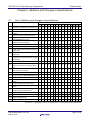
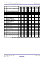
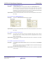
PG-FP5 V2.13 Flash Memory Programmer Release Note R20UT0689EJ0800 Rev.8.00 Mar 02, 2015 Thank you for purchasing the PG-FP5 flash memory programmer. This document describes specifications that have been added or changed, restrictions, and cautions on using the PG-FP5. Also see the user’s manual of the PG-FP5 for cautions on using the PG-FP5. See the following documents for restrictions related to the target device. • User’s manual of target device • Restriction notification document for target device Chapter 1 Product Version ........................................................................................................................ 2 Chapter 2 Additions and Changes to Specifications ................................................................................. 3 Chapter 3 Restrictions ............................................................................................................................. 14 R20UT0689EJ0800 Rev.8.00 Mar 02, 2015 Page 1 of 24 PG-FP5 V2.13 Flash Memory Programmer Release Note Chapter 1 Product Version Control Code Item No. Note 1 Firmware FPGA Programming GUI V1.00 V1 V1.00 2 V1.01 V1 V1.00 3 V2.00 V2 V2.00 4 V2.01 V2 V2.01 V2.02 V2 V2.02 V2.03 V2 V2.03 V2.04 V2 V2.03 V2.05 V2 V2.05 V2.06 V4 V2.06 10 V2.07 V4 V2.07 11 V2.09 V4 V2.09 12 V2.10 V4 V2.10 13 V2.11 V4 V2.11 14 V2.12 V4 V2.12 15 V2.13 V4 V2.13 1 A 5 Note 2 A, C 6 7 8 Note 2 A, C, D 9 Remark To check the version, follow the procedure below. • Firmware: On the menu bar, click Programmer, and then select Reset. • FPGA: On the menu bar, click Programmer, and then select Reset. • Programming GUI: On the menu bar, click Help, and then select About FP5.... Notes 1. The control code is the second digit from the left in the 10-digit serial number. If the product has been upgraded, a label indicating the new version is attached to the product and the x in V-UP x on this label indicates the control code. RENESAS Produced xxxx Control code D in this case PG-FP5 DC IN : 15V SERIAL NO. RD ******** Renesas Electronics 2. Products with control code A, C, and D are functionally equivalent. These products can be used in combination with the relevant version of the firmware, FPGA, and programming GUI. R20UT0689EJ0800 Rev.8.00 Mar 02, 2015 Page 2 of 24 PG-FP5 V2.13 Flash Memory Programmer Release Note Chapter 2 Additions and Changes to Specifications 2.1 No. List of additions and changes to specifications Additions and Changes to Specifications Product Version (Item No.) 1 2 3 4 5 6 7 8 9 10 11 12 13 14 15 1 Modification of Cancel button specification × 2 Addition of FP5 Manager functions × × 3 Addition of communication command functions × × 4 Addition of remote connector functions × × 5 Change of location of Erase memory before download check box Addition of specification related to Checksum command display × × × × Addition of program file size check function × × × Change of specification related to action log 9 × window view 10 Change of specification related to message × display view Addition of specification that enables 11 × specification of storage destination for ESF and PR5 files × × × × 6 7 8 Addition of [Enable target RESET] function 12 Addition of program file upload function 13 Change of GUI language to Japanese for Japanese version OS <Japanese version only> 14 Addition of specification of UART communication at 500 kbps × × × × × × × × 15 Addition of [Wide Voltage mode] function × × × × 16 Change of layout in Block protection area × × × × 17 Addition of HCUHEX file reading function 18 Addition of program file size monitoring function × × × × × × × × × × 19 Change of power button specification × Addition of [Disable FSW reprogramming] 20 × function 21 Addition of [OCD security ID setting] function × and [Option bytes setting] function × × × × × × × × × × × × × × × × 22 Support of 14-pin interface × × × × × × × × 23 Support of RL78 family × × × × × × × × 24 Support of RX600 series × × × × × × × × 25 Change of Windows supported × × × × × × × × −: Not relevant, ×: Specification change not implemented, : Specification change implemented R20UT0689EJ0800 Rev.8.00 Mar 02, 2015 Page 3 of 24 PG-FP5 V2.13 Flash Memory Programmer No. Release Note Additions and Changes to Specifications Product Version (Item No.) 1 2 3 4 5 6 7 8 9 10 11 12 13 14 15 26 Writing to 78K0 microcontrollers by using an × external UART clock × × × × × × × 27 Change of installer × × × × × × × × 28 Addition of device image file load function × × × × × × × × 29 Support of R8C family × × × × × × × × × 30 Support of SuperH family × × × × × × × × × 31 Change of installer × × × × × × × × × × 32 Change of file checksum function for RX family × × × × × × × × × × × 33 Addition of Minimum Programming function of data flash (V850E2/Fx4-L, V850E2/FF4-G, V850E2/FG4-G) × × × × × × × × × × × 34 Addition of Minimum Programming function of data flash (V850E2/Px4-L, V850E2/PG4-S) × × × × × × × × × × × × 35 Addition of unique code embedding function × × × × × × × × × × × × 36 Addition of a programming area setting for division into two parts × × × × × × × × × × × × 37 Addition of FINE programming function × × × × × × × × × × × × 38 Change of the sum calculation method for the file checksum function × × × × × × × × × × × × 39 Change of Windows supported × × × × × × × × × × × × × 40 Support of RH850 family, RX700 family (Include RX64x group) × × × × × × × × × × × × × 41 Change of a communications port name × × × × × × × × × × × × × 42 Support of Trusted Memory function × × × × × × × × × × × × × × 43 Addition of Minimum Programming function of data flash (RX (Except RX700, RX64x), RH850 (Except RH850/F1L) × × × × × × × × × × × × × × −: Not relevant, ×: Specification change not implemented, : Specification change implemented R20UT0689EJ0800 Rev.8.00 Mar 02, 2015 Page 4 of 24 PG-FP5 V2.13 Flash Memory Programmer 2.2 Release Note Details of additions and changes to specifications No. 1 Modification of Cancel button specification Description: The function of the Cancel button on the PG-FP5 main unit has been modified so that cancellation, which was applied to all commands, is only applied to the Read command. Implementation: This item has been implemented in products with control code A (firmware: V1.01, FPGA: V1, GUI: V1.00). No. 2 Addition of FP5 Manager functions Description: The following FP5 Manager functions have been added. • Password function • Upload disable function • Device setup disable function • Bank mode enable function • Simple mode enable function • Checksum compare function • Reset pin characteristics switch function Implementation: This item has been implemented in products with control code A (firmware: V2.00, FPGA: V2, GUI: V2.00). No. 3 Addition of communication command functions Description: The PG-FP5 main unit can now be manipulated via communication software by using communication commands, with the PG-FP5 connected to the host machine via the serial connector. Implementation: This item has been implemented in products with control code A (firmware: V2.00, FPGA: V2, GUI: V2.00). No. 4 Addition of remote connector functions Description: The PG-FP5 main unit can now be manipulated from remote locations by connecting an external control unit to the PG-FP5 via the remote connector. Remote operation enables manipulating and checking of programming and PASS/ERROR display from the external control unit. Implementation: This item has been implemented in products with control code A (firmware: V2.00, FPGA: V2, GUI: V2.00). R20UT0689EJ0800 Rev.8.00 Mar 02, 2015 Page 5 of 24 PG-FP5 V2.13 Flash Memory Programmer Release Note No. 5 Change of location of Erase memory before download check box Description: The location of the Erase memory before download check box has been moved from the Download file dialog box to the Object HEX file area on the Target tab in the Setup dialog box. Implementation: This item has been implemented in products with control code A (firmware: V2.00, FPGA: V2, GUI: V2.00). No. 6 Addition of specification related to Checksum command display Description: The checksum result is now displayed in the message display even while the Checksum command is being executed, either via the programming GUI or the command option during standalone operation. Implementation: This item has been implemented in products with control code A (firmware: V2.00, FPGA: V2, GUI: V2.00). No. 7 Addition of program file size check function Description: If the addresses of a downloaded program file are out of the address range set in the Operation mode area on the Standard tab in the Setup dialog box, the warning message WARNING: HEX file exceeds target device flash range. is now displayed in the action log window when the Program, Verify, or Autoprocedure(E.P.) command is executed. Implementation: This item has been implemented in products with control code A (firmware: V2.00, FPGA: V2, GUI: V2.00). No. 8 Addition of [Enable target RESET] function Description: The [Enable target RESET] function has been added. When this function is enabled, the RESET pin goes into input mode (Hi-Z), and the FP5 detects rising and falling edges input to the RESET pin immediately after executing a command. Implementation: This item has been implemented in products with control code A (firmware: V2.00, FPGA: V2, GUI: V2.00). No. 9 Change of specification related to action log window view Description: The message displayed in the action log window after command execution has been changed from OK to PASS. In addition, the error number is now displayed with the error message, as displayed in the message display. Implementation: This item has been implemented in products with control code A (firmware: V2.00, FPGA: V2, GUI: V2.00). R20UT0689EJ0800 Rev.8.00 Mar 02, 2015 Page 6 of 24 PG-FP5 V2.13 Flash Memory Programmer Release Note No. 10 Change of specification related to message display view Description: In conjunction with the addition of new functions in control code A (firmware: V2.00, FPGA: V2, GUI: V2.00), the display of all commands has been updated. Implementation: This item has been implemented in products with control code A (firmware: V2.00, FPGA: V2, GUI: V2.00). No. 11 Addition of specification that enables specification of storage destination for ESF and PR5 files Description: In products with control code A (firmware: V1.01, FPGA: V1, GUI: V1.00) or earlier, the ESF and PR5 files can only be stored in the FP5_PRJ folder where the programming GUI is installed, but these files can now be stored in any folder. Implementation: This item has been implemented in products with control code A (firmware: V2.00, FPGA: V2, GUI: V2.00). No. 12 Addition of program file upload function Description: A function to upload program files has been added. Uploading can be disabled by using an FP5 Manager function. Implementation: This item has been implemented in products with control code A (firmware: V2.00, FPGA: V2, GUI: V2.00). No. 13 Change of GUI language to Japanese for Japanese version OS <Japanese version only> Description: The GUI language has been changed to Japanese when used in a Japanese OS. Implementation: This item has been implemented in products with control code A (firmware: V2.01, FPGA: V2, GUI: V2.01). No. 14 Addition of specification of UART communication at 500 kbps Description: The specifications have been changed so that 500 kbps can now be selected as the baud rate of UART communication, even if a target device other than a 78K0R microcontroller is selected. However, communication at 500 kbps is not available if this specification is not supported in the target device. For the baud rate supported in each target device, see the user’s manual for the device or a supplementary document containing the parameter files. If a 78K0R microcontroller is used as the target device, communication at 500 kbps is available when using Programming GUI V1.00 and later. Implementation: This item has been implemented in products with control code A (firmware: V2.01, FPGA: V2, GUI: V2.01). R20UT0689EJ0800 Rev.8.00 Mar 02, 2015 Page 7 of 24 PG-FP5 V2.13 Flash Memory Programmer Release Note No. 15 Addition of Wide Voltage mode function Description: The Wide Voltage mode check box has been added to the Command options area. If this check box is selected, commands are executed in the wide voltage mode. If this check box is not selected, commands are executed in the full-speed mode. This check box is available when a device supporting this function is selected. For details about the wide voltage mode and full-speed mode, see the user’s manual of each device. Implementation: This item has been implemented in products with control code A (firmware: V2.02, FPGA: V2, GUI: V2.02). No. 16 Change of layout in Block protection area Description: The layout in the Block protection area has been changed. Before change After change Implementation: This item has been implemented in products with control code A (firmware: V2.02, FPGA: V2, GUI: V2.02). No. 17 Addition of HCUHEX file reading function Description: The HCUHEX files created using the HEX Consolidation Utility (HCU), which is used for generating ROM code for ordering Renesas Electronics preprogrammed flash memory devices, can now be read. Implementation: This item has been implemented in products with control code A, C (firmware: V2.03, FPGA: V2, GUI: V2.03). No. 18 Addition of program file size monitoring function Description: The Program file size monitor function check box has been added to the FP5 Manager dialog box. If this check box is selected, execution of the Program command is suspended if the program file is larger than the area to be written to. Implementation: This item has been implemented in products with control code A, C (firmware: V2.03, FPGA: V2, GUI: V2.03). R20UT0689EJ0800 Rev.8.00 Mar 02, 2015 Page 8 of 24 PG-FP5 V2.13 Flash Memory Programmer Release Note No. 19 Change of power button specification Description: The power of the PG-FP5 can now be turned on by pressing the POWER button for about 1 second. Implementation: This item has been implemented in products with control code A, C (firmware: V2.03, FPGA: V2, GUI: V2.03). No. 20 Addition of [Disable FSW reprogramming] function Description: The [Disable FSW reprogramming] function has been added. Implementation: This item has been implemented in products with control code A, C (firmware: V2.05, FPGA: V2, GUI: V2.05). No. 21 [OCD security ID setting] function and [Option bytes setting] function Description: The [OCD security ID setting] function and [Option bytes setting] function have been added. Implementation: This item has been implemented in products with control code A, C (firmware: V2.05, FPGA: V2, GUI: V2.05). No. 22 Support of 14-pin interface Description: A target cable (14pin type) compatible with the 14-pin interface of the E1 emulator will be provided in addition to the existing target cable (16pin type), starting from July 2011. Implementation: This item will be implemented in products with control code A, C, D (firmware: V2.06, FPGA: V4, GUI: V2.06). No. 23 Support of RL78 family Description: The RL78 family is now supported. In addition, a correspondence version may change with microcontrollers. Please refer to the release note of a parameter file. Implementation: This item has been implemented in products with control code A, C, D (firmware: V2.06, FPGA: V4, GUI: V2.06). No. 24 Support of RX600 series Description: The RX600 series is now supported. In addition, a correspondence version may change with microcontrollers. Please refer to the release note of a parameter file. Implementation: This item has been implemented in products with control code A, C, D (firmware: V2.06, FPGA: V4, GUI: V2.06). No. 25 Change of supported Windows Versions Description: The 32-bit and 64-bit editions of Windows 7 and the 64-bit edition of Windows Vista are now supported. Windows 2000 is no longer supported. Implementation: This item has been implemented in products with control code A, C, D (firmware: V2.06, FPGA: V4, GUI: V2.06). R20UT0689EJ0800 Rev.8.00 Mar 02, 2015 Page 9 of 24 PG-FP5 V2.13 Flash Memory Programmer Release Note No. 26 Writing to 78K0 microcontrollers by using an external UART clock Description: When writing to 78K0 microcontrollers by using UART communication, the PG-FP5 can now perform writing to a target system in which an external clock is input to the microcontroller's EXCLK pin. To enable this feature, select UART-EXCLK in the Port list box, select the On Target check box, and input the relevant frequency to the Frequency box. Along with the addition of this feature, the options in the Port list box have been changed as follows: UART-Ext-OSC → UART-X1-OSC (select when using an external resonator clock) UART-Ext-QB2CLK → UART-EXCLK (select when using an external clock or the FP5 clock) Implementation: This item has been implemented in products with control code A, C, D (firmware: V2.06, FPGA: V4, GUI: V2.06). No. 27 Change of installer Description: The installer has been changed to an installer for CS+. Implementation: This item has been implemented in products with control code A, C, D (firmware: V2.06, FPGA: V4, GUI: V2.06). No. 28 Addition of device image file load function Description: A function to enable loading of device image files (DDI files) supported by the Flash Development Toolkit has been added. Note that this function does not include a file-save capability. Note also that DDI files cannot be read by a hexadecimal editor. Implementation: This item has been implemented in products with control code A, C, D (firmware: V2.06, FPGA: V4, GUI: V2.06). No. 29 Support of R8C family Description: The R8C family is now supported. In addition, a correspondence version may change with microcontrollers. Please refer to the release note of a parameter file. Implementation: This item has been implemented in products with control code A, C, D (firmware: V2.07, FPGA: V4, GUI: V2.07). No. 30 Support of SuperH family Description: The SuperH family is now supported. In addition, a correspondence version may change with microcontrollers. Please refer to the release note of a parameter file. Implementation: This item has been implemented in products with control code A, C, D (firmware: V2.07, FPGA: V4, GUI: V2.07). R20UT0689EJ0800 Rev.8.00 Mar 02, 2015 Page 10 of 24 PG-FP5 V2.13 Flash Memory Programmer Release Note No. 31 Change of installer Description: The installer has been changed to a new installer. Implementation: This item has been implemented in products with control code A, C, D (firmware: V2.09, FPGA: V4, GUI: V2.09). No. 32 Change of file checksum function for RX family Description: The file checksum function is changed in accordance with the checksum command specification for RX family. With the checksum command specification for RX family, when ROM size is less than 8Kx2^n byte, a space area is complemented with FFh to an 8Kx2^n byte, and the range of an 8Kx2^n byte is calculated. Ex.1) When ROM size is 384 K bytes, a space area is complemented with FFh to a 512K byte, and the range of a 512K byte is calculated. Ex.2) When ROM size is 256 K bytes, a space area is complemented with FFh to 256 K bytes, and 256 K bytes of range is calculated. Implementation: This item has been implemented in products with control code A, C, D (firmware: V2.10, FPGA: V4, GUI: V2.10). No. 33 Addition of minimum unit programming function of data flash [Target MCU]: V850E2/Fx4-L, V850E2/FF4-G, V850E2/FG4-G Description: A minimum unit programming function for the data flash has been added. With minimum unit programming, Programming, verification, and reading of the area of the data flash that holds data proceeds in the minimum unit. It is effective if the [Enable minimum unit programming] check box is checked in the command option area of the device setup dialog [advance] tabbed page. While the minimum unit of programming was formerly the block, the PG-FP5 now supports all minimum units that an MCU handles in boot mode. For details on the minimum unit that an MCU handles in boot mode, refer to the corresponding hardware manual. Implementation: This item has been implemented in products with control code A, C, D (firmware: V2.10, FPGA: V4, GUI: V2.10). No. 34 Addition of minimum unit programming function of data flash [Target MCU]: V850E2/Px4-L, V850E2/PG4-S Description: A minimum unit programming function for the data flash has been added. With minimum unit programming, Programming, verification, and reading of the area of the data flash that holds data proceeds in the minimum unit. It is effective if the [Enable minimum unit programming] check box is checked in the command option area of the device setup dialog [advance] tabbed page. While the minimum unit of programming was formerly the block, the PG-FP5 now supports all minimum units that an MCU handles in boot mode. For details on the minimum unit that an MCU handles in boot mode, refer to the corresponding hardware manual. Implementation: This item has been implemented in products with control code A, C, D (firmware: V2.11, FPGA: V4, GUI: V2.11). R20UT0689EJ0800 Rev.8.00 Mar 02, 2015 Page 11 of 24 PG-FP5 V2.13 Flash Memory Programmer Release Note No. 35 Addition of unique code embedding function Description: A function for embedding unique codes in the specified area in a read program file has been added. Implementation: This item has been implemented in products with control code A, C, D (firmware: V2.11, FPGA: V4, GUI: V2.11). No. 36 Addition of a programming area setting for division into two parts Description: The ability to specify division into two parts (Area 0: 10 MB and Area 1: 6 MB) has been added to division patterns for programming area settings. Implementation: This item has been implemented in products with control code A, C, D (firmware: V2.11, FPGA: V4, GUI: V2.11). No. 37 Addition of FINE programming function [Target MCU]: RX100 and RX200 Description: Support for programming of RX100 and RX200 series MCUs via the FINE pin has been added. Implementation: This item has been implemented in products with control code A, C, D (firmware: V2.11, FPGA: V4, GUI: V2.11). No. 38 Change of the sum calculation method for the file checksum function [Target MCU]: The RX, SuperH and R8C of MCUs with data flash Description: The sum calculation method for the file checksum function was modified. Previous method: The sum is calculated for the code and data flash areas together at one time. New method: After the sum is calculated separately for the code flash area and data flash area, the results are added. NOTE: When the 32-bit arithmetic mode is selected, the checksum calculation results are the same between the previous and new methods, but when the 32-bit CRC mode is selected, the results will differ. Implementation: This item has been implemented in products with control code A, C, D (firmware: V2.11, FPGA: V4, GUI: V2.11). No. 39 Change of Windows supported Microcontroller: All Description: The 32-bit and 64-bit editions of Windows 8.1 are now supported. Windows XP is no longer supported. Implementation: This item has been implemented in products with control code A, C, D (firmware: V2.12, FPGA: V4, GUI: V2.12). R20UT0689EJ0800 Rev.8.00 Mar 02, 2015 Page 12 of 24 PG-FP5 V2.13 Flash Memory Programmer Release Note No. 40 Support of RH850 family, RX700 series (Include RX64x group) Microcontroller: RH850, RX700 (Include RX64x) Description: The RH850 family and RX700 series (Include RX64x group) are now supported. In addition, a correspondence version may change with microcontrollers. Please refer to the available microcontroller list. Implementation: This item has been implemented in products with control code A, C, D (firmware: V2.12, FPGA: V4, GUI: V2.12). No. 41 Change of a communications port name Microcontroller: RX (Except RX700, RX64x), SuperH Description: The item UART-ch0 in the [Port] list box under the [Standard] tab in the Device Setup dialog box has been changed to UART. Implementation: This item has been implemented in products with control code A, C, D (firmware: V2.12, FPGA: V4, GUI: V2.12). No. 42 Support of Trusted Memory function Microcontroller: RX700 (Include RX64x) Description: Support for Trusted Memory has been added. Implementation: This item has been implemented in products with control code A, C, D (firmware: V2.13, FPGA: V4, GUI: V2.13). No. 43 Addition of minimum unit programming function of data flash [Target MCU]: RX (Except RX700, RX64x), RH850 (Except RH850/F1L) Description: A minimum unit programming function for the data flash has been added. With minimum unit programming, Programming, verification, and reading of the area of the data flash that holds data proceeds in the minimum unit. It is effective if the [Enable minimum unit programming] check box is checked in the device setup dialog [advance] tabbed page. While the minimum unit of programming was formerly the block, the PG-FP5 now supports all minimum units that an MCU handles in boot mode. For details on the minimum unit that an MCU handles in boot mode, refer to the corresponding hardware manual. Implementation: This item has been implemented in products with control code A, C, D (firmware: V2.13, FPGA: V4, GUI: V2.13). R20UT0689EJ0800 Rev.8.00 Mar 02, 2015 Page 13 of 24 PG-FP5 V2.13 Flash Memory Programmer Release Note Chapter 3 Restrictions 3.1 Restriction List No. Restrictions 1 2 3 4 5 6 7 8 9 10 11 12 13 14 15 16 Restriction whereby Invalid Device Port is displayed Restriction whereby standalone operation can no longer be performed under specific conditions Restriction whereby erase is performed even if Erase memory before download is not selected Restriction whereby status bar is displayed incorrectly Restriction whereby RESET pin is always pulled up to 5 V when Run after Disconnect is set Restriction whereby no clock is supplied when FP5CLK is selected for pseudo 3-wire 2 communication or I C communication Restriction whereby Motorola S type program file is not displayed in the list box Restriction whereby FLMD0 pin outputs low level when 78K0S (single-wire UART) is used Restriction whereby lowercase letters are illegally converted to uppercase letters when upprm or upset command is executed Restriction whereby an invalid checksum result is obtained if a program file is downloaded in Simple mode Restriction whereby bank switching for the program file cannot be specified in bank mode Restriction on reading a Motorola S1-record hex format program file Restriction related to installation of USB driver Restriction whereby the error NAND flash Mapping Error is displayed Restriction whereby the message display is not updated Restriction which cannot get the flash options of RL78 17 Restriction on reading out data from R8C 18 Restriction which cannot download the parameter file in simple mode Product Version (Item No.) 1 2 3 4 5 6 7 8 9 10 11 12 13 14 15 × × × × × × × × × × × × × × × × × × − − × − − × × × × × × − − − − × × × × × × × × × × × × × × × × × × × × × × × × × × × × × × × × × × × × × × × × × −: Not relevant, ×: Applicable, : Corrected R20UT0689EJ0800 Rev.8.00 Mar 02, 2015 Page 14 of 24 PG-FP5 V2.13 Flash Memory Programmer No. Release Note Restrictions Product Version (Item No.) 1 2 3 4 5 6 7 8 9 10 11 12 13 14 15 × × × × × × × × × × × 20 Restriction of file checksum function × Restriction on errors in the downloading of 21 × program files 22 Restriction on display in response to the file − checksum command × × × × × × × × × × × × × × × × × × × × × × − − − − − − − × × × × 19 Restriction of Checksum comparison function 23 Restriction on the read (display) command × × × × × × × × × × × × × 24 Restriction on the unique code 25 Restriction on the specified address of the unique code 26 Restriction of Minimum Programming function of data flash 27 Restriction on IO signal settings when FINE communications are selected 28 Restriction on command for acquiring flash options (RX200 Series, RX600 Series) 29 Restriction on acquisition command of flash options (SuperH Family) 30 Restriction with Option Bytes and OCD Security ID Settings 31 Restriction with Downloading Program Files in Code Flash Area 32 Restriction with Downloading Program Files in Data Flash Area 33 Restriction related to program files that include data for the option setting memory 34 Restriction on changing settings related to ESF files − − − − − − − − − − − − × − − − − − − − − − − − − × − − − − − − − − − − − × × − − − − − − − − − − − − × − − − − − − − − − − − − × − − − − − − − − − − − − × − − − − − − − − − − − − × − − − − − − − − − − − − × − − − − − − − − − − − − × − − − − − − − − − − − − − × × × × × × × × × × × × × × × × −: Not relevant, ×: Applicable, : Corrected R20UT0689EJ0800 Rev.8.00 Mar 02, 2015 Page 15 of 24 PG-FP5 V2.13 Flash Memory Programmer 3.2 Release Note Restriction Details No. 1 Restriction whereby Invalid Device Port is displayed Description: When a PR5 file is downloaded, the message Invalid Device Port might be displayed in the action log window. After that, PR5 files can no longer be downloaded correctly. Workaround: There is no workaround. Action: This issue has been corrected in products with control code A (firmware: V2.00, FPGA: V2, GUI: V2.00). No. 2 Restriction whereby standalone operation can no longer be performed under specific conditions Description: If command execution is continued by using control buttons on the PG-FP5 main unit while the Programming GUI is not running, the message ERROR: 800 Res. by Watchdog is displayed in the message display on the PG-FP5 main unit and the subsequent operations might no longer be able to be performed. Workaround: There is no workaround. When this situation occurs, control of the POWER button is also unavailable. Therefore, disconnect the AC adapter and connect it again to restart the PG-FP5. Action: This issue has been corrected in products with control code A (firmware: V1.01, FPGA: V1, GUI: V1.00). No. 3 Restriction whereby erase is performed even if Erase memory before download is not selected Description: Erase is performed even if the Erase memory before download check box is not selected in the Download file dialog box, which is opened via the Object HEX file area on the Target tab in the Setup dialog box. Workaround: There is no workaround. Action: This issue has been corrected in products with control code A (firmware: V2.00, FPGA: V2, GUI: V2.00). No. 4 Restriction whereby status bar is displayed incorrectly Description: The status bar is displayed incorrectly in the following cases: (1) An error is displayed erroneously if it takes five or more seconds for SUM data to be returned during Checksum command execution. (2) PASS is displayed erroneously if the code flash is verified to be OK but the data flash is reported as having an error. Workaround: There is no workaround. Action: This issue has been corrected in products with control code A (firmware: V2.00, FPGA: V2, GUI: V2.00). R20UT0689EJ0800 Rev.8.00 Mar 02, 2015 Page 16 of 24 PG-FP5 V2.13 Flash Memory Programmer Release Note No. 5 Restriction whereby RESET pin is always pulled up to 5 V when Run after Disconnect is set Description: The RESET pin of the PG-FP5 must go into the Hi-Z state when Run after Disconnect is set, but it is pulled up to 5 V. Workaround: There is no workaround. Action: This issue has been corrected in products with control code A (firmware: V2.00, FPGA: V2, GUI: V2.00). No. 6 Restriction whereby no clock is supplied when FP5CLK is selected for pseudo 3-wire communication or 2 I C communication 2 Description: No clock is supplied when FP5CLK is selected for pseudo 3-wire communication or I C communication. Workaround: There is no workaround. Action: This issue has been corrected in products with control code A (firmware: V2.00, FPGA: V2, GUI: V2.00). No. 7 Restriction whereby Motorola S type program file is not displayed in the list box Description: When a program file of Motorola S type (except for *.hex and *.rec) is selected in the Download file dialog box which is opened via the Object HEX file area on the Target tab in the Setup dialog box, the file is not displayed in the list box in the Object HEX file area. Workaround: There is no workaround. Action: This issue has been corrected in products with control code A (firmware: V2.00, FPGA: V2, GUI: V2.00). No. 8 Restriction whereby FLMD0 pin outputs low level when 78K0S (single-wire UART) is used Description: If the CLK and FLMD0 pins are shorted in the target system when 78K0S (single-wire UART) is used, the FLMD0 pin that should output Hi-Z incorrectly outputs a low level, which disturbs programming. (This restriction is applicable only when a microcontroller that uses the FLMD0 pin was used before using 78K0S (single-wire UART).) Workaround: Execute the Reset command of the PG-FP5 or turn off and then on the PG-FP5 power before using 78K0S (single-wire UART); the FLMD0 pin afterward outputs Hi-Z. Action: This issue has been corrected in products with control code A (firmware: V2.00, FPGA: V2, GUI: V2.00). R20UT0689EJ0800 Rev.8.00 Mar 02, 2015 Page 17 of 24 PG-FP5 V2.13 Flash Memory Programmer Release Note No. 9 Restriction whereby lowercase letters are illegally converted to uppercase letters when upprm or upset command is executed Description: The letter “a” in the format version is illegally converted to “A” when the upprm command is executed. The extensions of parameter files are illegally converted to uppercase letters when the upset command is executed. Use of the files created by these commands does not cause any problems. Workaround: There is no workaround. Action: This issue has been corrected in products with control code A (firmware: V2.01, FPGA: V2, GUI: V2.01). No. 10 Restriction whereby an invalid checksum result is obtained if a program file is downloaded in Simple mode Description: If a program file that includes data flash is downloaded in Simple mode, the checksum result to be displayed in the message display on the PG-FP5 main unit, which should indicate the checksum of the code flash and data flash areas, indicates the checksum of the code flash area only. Workaround: There is no workaround. Action: This issue has been corrected in products with control code A (firmware: V2.01, FPGA: V2, GUI: V2.01). No. 11 Restriction whereby bank switching for the program file cannot be specified in bank mode Description: When the PG-FP5 runs in bank mode and if a programming area is selected via a bank signal from the remote connector, the programming area selected via the bank signal should usually be selected, but the program file in the programming area selected by the Programming GUI is selected. The settings selected via the bank signal are then applied to PR5 and ESF files. Example: Programming area number selected by Programming GUI: 0 Programming area number selected via bank signal: 1 In this case, PR5 and ESF files in programming area 1 and the program file in programming area 0 are specified. Workaround: There is no workaround. Action: This issue has been corrected in products with control code A (firmware: V2.01, FPGA: V2, GUI: V2.01). No. 12 Restriction on reading a Motorola S1-record hex format program file Description: If a program file in the Motorola S1-record hex format is read to the FP5, program files saved in the specified programming area become invalid. Workaround: There is no workaround. Action: This issue has been corrected in products with control code A or C (firmware: V2.03, FPGA: V2, GUI: V2.03). R20UT0689EJ0800 Rev.8.00 Mar 02, 2015 Page 18 of 24 PG-FP5 V2.13 Flash Memory Programmer Release Note No. 13 Restriction related to installation of USB driver Description: If a PG-FP5 unit is connected to a USB port to which another FP5 unit with a different serial number was connected on the same host, the USB driver is not automatically recognized and installation of the USB driver is requested. Workaround: There is no workaround. Action: This issue has been corrected in products with control code A or C (firmware: V2.03, FPGA: V2, GUI: V2.03). No. 14 Restriction whereby the error NAND flash - Mapping Error is displayed Description: If the PG-FP5 is used continuously while conditions (1) and (2) below are satisfied, the error below might be displayed in the action log window when a program file is downloaded or a writing command is executed. (1) A program file that has a cluster of FFh data that is 16 KB or longer is used. (2) The program file described in (1) is frequently downloaded. Displayed error: *** System Error(s), Warning(s): Warning: NAND flash - Mapping Error Even if the above error is displayed, downloading the program or executing the Program command is performed correctly. Workaround: There is no workaround. Action: This issue has been corrected in products with control code A or C (firmware: V2.04, FPGA: V2, GUI: V2.03). No. 15 Restriction whereby the message display is not updated Description: The writing status shown in the message display on the PG-FP5 unit might freeze and no longer be updated. (Even if this problem occurs, a command that downloads or writes a program runs normally.) Workaround: There is no workaround. Action: This issue has been corrected in products with control code A or C (firmware: V2.04, FPGA: V2, GUI: V2.03). No. 16 Restriction which cannot get the flash options of RL78 Description: If the PG-FP5 executes Get Flash options command to RL78 valid of security setting, E1601 Protect error. is displayed, the PG-FP5 cannot get the flash options. Action: This issue has been corrected in products with control code A, C or D (firmware: V2.07, FPGA: V4, GUI: V2.07). R20UT0689EJ0800 Rev.8.00 Mar 02, 2015 Page 19 of 24 PG-FP5 V2.13 Flash Memory Programmer Release Note No. 17 Restriction on reading out data from R8C Description: When you read out data from flash memory in R8C, the address mapping of the data flash area is saved incorrectly if you click the Read and then the Write Intel HEX file command. Note that even if this problem arises, no error message is displayed, so do not use the data saved in the Intel format. Workaround: To read out data from flash memory, do not click the Write Intel HEX file command, but the Write Motorola SREC file. Action: This issue has been corrected in products with control code A, C or D (firmware: V2.09, FPGA: V4, GUI: V2.09). No. 18 Restriction which cannot download the parameter file in simple mode Description: When a parameter file is downloaded by simple mode, "ERROR (E009): HEX file contains invalid data!! " may occur and may be unable to download. Workaround: Push the clear button in a device setup dialog [target] tab, and make programming area a clear. Action: This issue has been corrected in products with control code A, C or D (firmware: V2.09, FPGA: V4, GUI: V2.09). No. 19 Restriction of Checksum comparison function Microcontroller: V850E2/Fx4-L, V850E2/FF4-G, V850E2/FG4-G, V850E2/Px4-L, V850E2/PG4-S Description: If a checksum comparison function is enabled and a checksum command is executed, a checksum value will be displayed correctly, but in Checksum compare, the address range of a data flash is mistaken and Checksum compare becomes an error. Workaround: There is no workaround. Action: This issue has been corrected in products with control code A, C or D (firmware: V2.10, FPGA: V4, GUI: V2.10). No. 20 Restriction of file checksum function Microcontroller: V850E2/Px4-L Description: The value of start/end address of a data flash is not right at [Device Area] selection of a checksum dialog. Workaround: Please select a [User Defined]. The right address is set up as an initial value. Action: This issue has been corrected in products with control code A, C or D (firmware: V2.11, FPGA: V4, GUI: V2.11). R20UT0689EJ0800 Rev.8.00 Mar 02, 2015 Page 20 of 24 PG-FP5 V2.13 Flash Memory Programmer Release Note No. 21 Restriction on errors in the downloading of program files Description: Downloading of a program file satisfying the condition below may lead to defective communications between the programming GUI and the PG-FP5 body. In such cases, [Error] is displayed in the status bar of the programing GUI. Condition: Program file having a data record length of 250 bytes or more Workaround: Action: Make compiler settings such that the length of the data records is less than 250 bytes.. This issue has been corrected in products with control code A, C or D (firmware: V2.11, FPGA: V4, GUI: V2.11). No. 22 Restriction on display in response to the file checksum command Microcontroller: RX, SuperH, and R8C Description: When the file checksum command is executed, the display in the [File checksum] area of the programming parameter window is not correct. Workaround: Refer to the action log window for the results of the file checksum operation. Action: This issue has been corrected in products with control code A, C or D (firmware: V2.11, FPGA: V4, GUI: V2.11). No. 23 Restriction on the read (display) command Microcontroller: V850 products equipped with data flash memory and ID tags Description: When the [Read (display)] command is executed after an operation mode that excludes block 0 of the data flash memory has been set, reading proceeds at a different address from that displayed in the action log window. Workaround: There is no workaround. Action: This issue has been corrected in products with control code A, C or D (firmware: V2.12, FPGA: V4, GUI: V2.12). No. 24 Restriction on the unique code Microcontroller: V850 products equipped with data flash memory and ID tags Description: When the unique code embedding function is executed after an operation mode that excludes block 0 of the data flash memory has been set, the code is embedded at an illegal address. Workaround: There is no workaround. Action: This issue has been corrected in products with control code A, C or D (firmware: V2.12, FPGA: V4, GUI: V2.12). No. 25 Restriction on the specified address of the unique code Description: When the unique code embedding function is used and the address where the unique code is embedded is within the range from FFFFFF00h to FFFFFFFFh, the unique code is not embedded in the address range from FFFFFF00h to FFFFFFFFh. Workaround: There is no workaround. Action: This issue has been corrected in products with control code A, C or D (firmware: V2.12, FPGA: V4, GUI: V2.12). R20UT0689EJ0800 Rev.8.00 Mar 02, 2015 Page 21 of 24 PG-FP5 V2.13 Flash Memory Programmer Release Note No. 26 Restriction of Minimum Programming function of data flash Microcontroller: V850E2/Fx4-L, V850E2/FF4-G, V850E2/FG4-G, V850E2/Px4-L, V850E2/PG4-S Description: When a program file extending beyond the address range of the flash memory is selected and the minimum programming function is enabled, the programming GUI does not operate normally. Workaround: There is no workaround. If programming has proceeded with the above settings, restart the programming GUI. Then, the program is restarted with the setting for the minimum programming function disabled. Action: This issue has been corrected in products with control code A, C or D (firmware: V2.12, FPGA: V4, GUI: V2.12). No. 27 Restriction on IO signal settings when FINE communications are selected Microcontroller: RX200 Description: When FINE communications are selected, the display indicates that the [IO signal setting] area is editable. Note that IO 0, 1, 2, 4, and 5 pins are always high impedance and the IO3 pin is used to communicate with the FINE pin regardless of the settings, so the settings have no effect on operation. Workaround: There is no workaround. Action: This issue has been corrected in products with control code A, C or D (firmware: V2.12, FPGA: V4, GUI: V2.12). No. 28 Restriction on command for acquiring flash options Microcontroller: RX200, RX600 Description: The flash option acquisition command cannot correctly obtain the lock bit settings. Workaround: Use the glb communication command to handle acquisition. Action: This issue has been corrected in products with control code A, C or D (firmware: V2.12, FPGA: V4, GUI: V2.12). No. 29 Restriction on acquisition command of flash options Microcontroller: SuperH Description: When an MCU that does not include the lock bit function is in use, the [Flash option acquisition] command and glb communication command are executable. However, executing either leads to an error. Workaround: There is no workaround. Action: This issue has been corrected in products with control code A, C or D (firmware: V2.12, FPGA: V4, GUI: V2.12). R20UT0689EJ0800 Rev.8.00 Mar 02, 2015 Page 22 of 24 PG-FP5 V2.13 Flash Memory Programmer Release Note No. 30 Restriction with Option Bytes and OCD Security ID Settings Microcontroller: V850E2/Fx4-L, V850E2/FF4-G, V850E2/FG4-G, V850E2/Px4-L, V850E2/PG4-S Description: If the conditions described in below are met, changed values are not saved in ESF files. The values of the option bytes and OCD security ID previously saved are, therefore, downloaded to the PG-FP5. Conditions: The problem occurs when all of the following conditions are met: (1) The minimum unit programming function for the data flash memory is enabled. (2) Downloading to the PG-FP5 proceeds after the values of the option bytes and OCD security ID are changed. Workaround: To ensure that changed values of the option bytes and OCD security ID are saved, change the values while the minimum unit programming function for the data flash memory is disabled. Enable the minimum unit programming function after that. Action: This issue has been corrected in products with control code A, C or D (firmware: V2.12, FPGA: V4, GUI: V2.12). No. 31 Restriction with Downloading Program Files in Code Flash Area Microcontroller: V850E2/Fx4-L, V850E2/FF4-G, V850E2/FG4-G Description: If a program file is downloaded to the PG-FP5 under the conditions described in below, incorrect data is downloaded in the code flash area. Even if incorrect data is downloaded, however, no error messages appear. Conditions: The problem occurs when all of the following conditions are met: (1) The minimum unit programming function for the data flash memory is enabled. (2) The program file for downloading is the one in Intel HEX format. (3) The program file for downloading includes data for both the code flash and data flash memory. Workaround: There is no workaround. Action: This issue has been corrected in products with control code A, C or D (firmware: V2.12, FPGA: V4, GUI: V2.12). R20UT0689EJ0800 Rev.8.00 Mar 02, 2015 Page 23 of 24 PG-FP5 V2.13 Flash Memory Programmer Release Note No. 32 Restriction with Downloading Program Files in Data Flash Area Microcontroller: V850E2/Px4-L, V850E2/PG4-S Description: If a program file is downloaded to the PG-FP5 under the conditions described in below, incorrect data may be downloaded in the data flash area. Even if incorrect data is downloaded, however, error messages do not necessarily appear. Conditions: The problem occurs when all of the following conditions are met: (1) The minimum unit programming function for the data flash memory is enabled. (2) The program file for downloading includes data for both the code flash and data flash memory. Workaround: Only download a program file to the PG-FP5 after disabling the minimum unit programming function for the data flash memory. When downloading a program file that includes data for both the code flash and data flash memory to the PG-FP5, the minimum unit programming function cannot be used. Action: This issue has been corrected in products with control code A, C or D (firmware: V2.12, FPGA: V4, GUI: V2.12). No. 33 Restriction related to program files that include data for the option setting memory Microcontroller: RX700 (Include RX64x) Description: The PG-FP5 does not read data in the option setting memory even when it reads a program file that includes data for the option setting memory. Workaround: Use the [Standard] tab in Device Setup dialog box to set the option setting memory. Action: This issue has been corrected in products with control code A, C or D (firmware: V2.13, FPGA: V4, GUI: V2.13). The earlier menu item for making such settings by using dialog boxes has been deleted. Be sure that program files to be read contain data for the option setting memory area. No. 34 Restriction on changing settings related to ESF files Description: When any setting in the Setup dialog box is changed to select a state in which modification of ESF files is disabled, ESF files are not modified, but no error occurs. Modification of ESF files is disabled, for example, in the following cases. E.g. (1) A user who does not have the privilege to modify files due to the security setting for the folder where ESF files are saved attempts to do so through the programming GUI. E.g. 2) Read-only is selected as the property of ESF files. Workaround: In case 1, copy the ESF files to any folder where modification is allowed. In case 2, deselect the read-only checkbox. Action: In planning. All trademarks and registered trademarks are the property of their respective owners. R20UT0689EJ0800 Rev.8.00 Mar 02, 2015 Page 24 of 24 Notice 1. Descriptions of circuits, software and other related information in this document are provided only to illustrate the operation of semiconductor products and application examples. You are fully responsible for the incorporation of these circuits, software, and information in the design of your equipment. Renesas Electronics assumes no responsibility for any losses incurred by you or third parties arising from the use of these circuits, software, or information. 2. Renesas Electronics has used reasonable care in preparing the information included in this document, but Renesas Electronics does not warrant that such information is error free. Renesas Electronics 3. Renesas Electronics does not assume any liability for infringement of patents, copyrights, or other intellectual property rights of third parties by or arising from the use of Renesas Electronics products or assumes no liability whatsoever for any damages incurred by you resulting from errors in or omissions from the information included herein. technical information described in this document. No license, express, implied or otherwise, is granted hereby under any patents, copyrights or other intellectual property rights of Renesas Electronics or others. 4. You should not alter, modify, copy, or otherwise misappropriate any Renesas Electronics product, whether in whole or in part. Renesas Electronics assumes no responsibility for any losses incurred by you or 5. Renesas Electronics products are classified according to the following two quality grades: "Standard" and "High Quality". The recommended applications for each Renesas Electronics product depends on third parties arising from such alteration, modification, copy or otherwise misappropriation of Renesas Electronics product. the product's quality grade, as indicated below. "Standard": Computers; office equipment; communications equipment; test and measurement equipment; audio and visual equipment; home electronic appliances; machine tools; personal electronic equipment; and industrial robots etc. "High Quality": Transportation equipment (automobiles, trains, ships, etc.); traffic control systems; anti-disaster systems; anti-crime systems; and safety equipment etc. Renesas Electronics products are neither intended nor authorized for use in products or systems that may pose a direct threat to human life or bodily injury (artificial life support devices or systems, surgical implantations etc.), or may cause serious property damages (nuclear reactor control systems, military equipment etc.). You must check the quality grade of each Renesas Electronics product before using it in a particular application. You may not use any Renesas Electronics product for any application for which it is not intended. Renesas Electronics shall not be in any way liable for any damages or losses incurred by you or third parties arising from the use of any Renesas Electronics product for which the product is not intended by Renesas Electronics. 6. You should use the Renesas Electronics products described in this document within the range specified by Renesas Electronics, especially with respect to the maximum rating, operating supply voltage range, movement power voltage range, heat radiation characteristics, installation and other product characteristics. Renesas Electronics shall have no liability for malfunctions or damages arising out of the use of Renesas Electronics products beyond such specified ranges. 7. Although Renesas Electronics endeavors to improve the quality and reliability of its products, semiconductor products have specific characteristics such as the occurrence of failure at a certain rate and malfunctions under certain use conditions. Further, Renesas Electronics products are not subject to radiation resistance design. Please be sure to implement safety measures to guard them against the possibility of physical injury, and injury or damage caused by fire in the event of the failure of a Renesas Electronics product, such as safety design for hardware and software including but not limited to redundancy, fire control and malfunction prevention, appropriate treatment for aging degradation or any other appropriate measures. Because the evaluation of microcomputer software alone is very difficult, please evaluate the safety of the final products or systems manufactured by you. 8. Please contact a Renesas Electronics sales office for details as to environmental matters such as the environmental compatibility of each Renesas Electronics product. Please use Renesas Electronics products in compliance with all applicable laws and regulations that regulate the inclusion or use of controlled substances, including without limitation, the EU RoHS Directive. Renesas Electronics assumes no liability for damages or losses occurring as a result of your noncompliance with applicable laws and regulations. 9. Renesas Electronics products and technology may not be used for or incorporated into any products or systems whose manufacture, use, or sale is prohibited under any applicable domestic or foreign laws or regulations. You should not use Renesas Electronics products or technology described in this document for any purpose relating to military applications or use by the military, including but not limited to the development of weapons of mass destruction. When exporting the Renesas Electronics products or technology described in this document, you should comply with the applicable export control laws and regulations and follow the procedures required by such laws and regulations. 10. It is the responsibility of the buyer or distributor of Renesas Electronics products, who distributes, disposes of, or otherwise places the product with a third party, to notify such third party in advance of the contents and conditions set forth in this document, Renesas Electronics assumes no responsibility for any losses incurred by you or third parties as a result of unauthorized use of Renesas Electronics products. 11. This document may not be reproduced or duplicated in any form, in whole or in part, without prior written consent of Renesas Electronics. 12. Please contact a Renesas Electronics sales office if you have any questions regarding the information contained in this document or Renesas Electronics products, or if you have any other inquiries. (Note 1) "Renesas Electronics" as used in this document means Renesas Electronics Corporation and also includes its majority-owned subsidiaries. (Note 2) "Renesas Electronics product(s)" means any product developed or manufactured by or for Renesas Electronics. http://www.renesas.com SALES OFFICES Refer to "http://www.renesas.com/" for the latest and detailed information. Renesas Electronics America Inc. 2801 Scott Boulevard Santa Clara, CA 95050-2549, U.S.A. Tel: +1-408-588-6000, Fax: +1-408-588-6130 Renesas Electronics Canada Limited 9251 Yonge Street, Suite 8309 Richmond Hill, Ontario Canada L4C 9T3 Tel: +1-905-237-2004 Renesas Electronics Europe Limited Dukes Meadow, Millboard Road, Bourne End, Buckinghamshire, SL8 5FH, U.K Tel: +44-1628-585-100, Fax: +44-1628-585-900 Renesas Electronics Europe GmbH Arcadiastrasse 10, 40472 Düsseldorf, Germany Tel: +49-211-6503-0, Fax: +49-211-6503-1327 Renesas Electronics (China) Co., Ltd. Room 1709, Quantum Plaza, No.27 ZhiChunLu Haidian District, Beijing 100191, P.R.China Tel: +86-10-8235-1155, Fax: +86-10-8235-7679 Renesas Electronics (Shanghai) Co., Ltd. Unit 301, Tower A, Central Towers, 555 Langao Road, Putuo District, Shanghai, P. R. China 200333 Tel: +86-21-2226-0888, Fax: +86-21-2226-0999 Renesas Electronics Hong Kong Limited Unit 1601-1611, 16/F., Tower 2, Grand Century Place, 193 Prince Edward Road West, Mongkok, Kowloon, Hong Kong Tel: +852-2265-6688, Fax: +852 2886-9022 Renesas Electronics Taiwan Co., Ltd. 13F, No. 363, Fu Shing North Road, Taipei 10543, Taiwan Tel: +886-2-8175-9600, Fax: +886 2-8175-9670 Renesas Electronics Singapore Pte. Ltd. 80 Bendemeer Road, Unit #06-02 Hyflux Innovation Centre, Singapore 339949 Tel: +65-6213-0200, Fax: +65-6213-0300 Renesas Electronics Malaysia Sdn.Bhd. Unit 1207, Block B, Menara Amcorp, Amcorp Trade Centre, No. 18, Jln Persiaran Barat, 46050 Petaling Jaya, Selangor Darul Ehsan, Malaysia Tel: +60-3-7955-9390, Fax: +60-3-7955-9510 Renesas Electronics India Pvt. Ltd. No.777C, 100 Feet Road, HALII Stage, Indiranagar, Bangalore, India Tel: +91-80-67208700, Fax: +91-80-67208777 Renesas Electronics Korea Co., Ltd. 12F., 234 Teheran-ro, Gangnam-Gu, Seoul, 135-080, Korea Tel: +82-2-558-3737, Fax: +82-2-558-5141 © 2015 Renesas Electronics Corporation. All rights reserved. Colophon 5.0