1
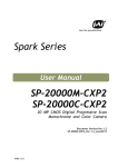
SP-5000M-CXP2 / SP-5000C-CXP2
- Contents Introduction .....................................................................................1. General .....................................................................................2. Camera composition ....................................................................3. Main features ............................................................................4. Locations and functions ...............................................................4.1
4.2
67789-
Locations and functions ............................................................................. - 9 Rear panel ............................................................................................- 10 -
5. Input and output.......................................................................... - 11 5.1 CoaXpress interface ................................................................................- 11
5.1.1 CoaXPress interface standard ................................................................- 11
5.1.2 CoaXpress interface used in SP-5000-CXP2 ................................................- 11
5.1.3 The relationship between sensor bit, pixel clock and output format. ...............- 13
5.1.4 Associated GenICam register ................................................................- 13
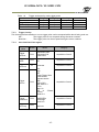
5.2 Connectors and pin assignment...................................................................- 14
5.2.1 Digital Video Output (75Ω 1.0・2.3 DIN Receptacle) ..................................- 14
5.2.2
12-Pin connector ..............................................................................- 14
5.2.3 AUX Standard
Hirose 10-Pin connector ................................................- 15
5.2.3.1 Figure and pin configuration............................................................- 15
5.2.4 AUX Type 2 HIROSE 10-Pin connector (factory option) ..................................- 15
5.2.5 AUX Type 3 HIROSE 10-Pin connector (factory option) ................................- 16
5.3 Digital IN/OUT interface ...........................................................................- 16
5.3.1 Line Selector ....................................................................................- 16
5.3.2 Line Source......................................................................................- 17
5.3.3 Line Mode .......................................................................................- 17
5.3.4 Line Inverter ....................................................................................- 17
5.3.5 Line Status ......................................................................................- 17
5.3.6 Line Format .....................................................................................- 17
5.3.7 GPIO ..............................................................................................- 17
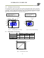
5.3.7.1 Basic block diagram ......................................................................- 18
5.3.7.2 IN and OUT matrix table.................................................................- 19
5.3.8 Associated GenIcam register .................................................................- 20
5.4 Pulse Generator .....................................................................................- 20
5.4.1 Clock Pre-scaler ................................................................................- 21
5.4.2 Pulse Generator Selector .....................................................................- 21
5.4.3 Pulse Generator Length .......................................................................- 22
5.4.4 Pulse Generator Start Point ..................................................................- 22
5.4.5 Pulse Generator End Point ...................................................................- 22
5.4.6 Pulse Generator Repeat Count ..............................................................- 22
5.4.7 Pulse Generator Clear Activation ...........................................................- 22
5.4.8 Pulse Generator Clear Sync Mode ...........................................................- 22
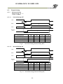
5.4.9 Pulse Generator Clear Source................................................................- 24
5.4.10 Pulse Generator Inverter ....................................................................- 25
5.4.11 Pulse Generator Setting Parameters ......................................................- 25
5.4.12 Associated GenICam register ...............................................................- 26
-
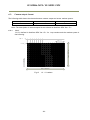
6.1 Sensor layout ........................................................................................- 27
6.1.1 Monochrome sensor............................................................................- 27
6.1.2
Bayer color sensor ............................................................................- 27
6.2. Camera output format ............................................................................- 28
6.2.1 1X-1Y .............................................................................................- 28
-
6.
Sensor layout, output format and timing ........................................ - 27 -
-3-