1
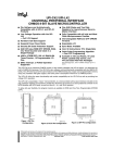
HMOS Single-Component 8-Bit Microcomputer
• High Performance HMOS
• Interval Timer/Event Counter
• Two Single Level Interrupts
• Single 5-Volt Supply
• Over 96 Instructions; 90% Single Byte
• Reduced Power Consumption
• Compatible with 8080/8085 Peripherals
• Easily Expandable Memory and I/O
• Up to 1.36 µs Instruction Cycle
All Instructions 1 or 2 Cycles
The Intel MCS®-48 family are totally self-sufficient, 8-bit parallel computers fabricated on single silicon chips using
Intel's advanced N-channel silicon gate HMOS process.
The family contains 27 I/O lines, an 8-bit timer/counter and on-board oscillator/clock circuits. For systems that
require extra capability, the family can be expanded using MCS®-80/MCS®-85 peripherals.
To minimize development problems and provide maximum flexibility, a logically and functionally pin-compatible
version of the ROM devices with UV-erasable user-programmable EPROM program memory is available with
minor differences.
These microcomputers are designed to be efficient controllers as well as arithmetic processors. They have
extensive bit handling capability as well as facilities for both binary and BCD arithmetic. Efficient use of program
memory results from an instruction set consisting mostly of single byte instructions and no instructions over 2
bytes in length.
Device
CLOCK
Internal Memory
RAM Standby
8050AH
4K x 8 ROM
256 x 8 RAM
yes
8049H
2K x 8 ROM
128 x 8 RAM
yes
8048H
1K x 8 ROM
64 x 8 RAM
yes
8040AHL
none
256 x 8 RAM
yes
8039HL
none
128 x 8 RAM
yes
8035HL
none
64 x 8 RAM
yes
8749H
2K x 8 EPROM
128 x 8 RAM
yes
8748H
1K x 8 EPROM
64 x 8 RAM
yes
PROGRAM
MEMORY
DATA
MEMORY
8
XTAL
SINGLE
STEP
8048H
8748H
8035HL
8049H
8749H
8050AH
8040AHL
EXTERNAL
MEM
TEST
8 BIT
TIMER/
EVENT COUNTER
27
I/O LINES
Figure 1.
Block Diagram
READ
WRITE
PROGRAM
STORE
ENABLE
ADDRESS
LATCH
ENABLE
INTERRUPT
BUS
PORT
2
8
RESET
8 BIT
CPU
PORT
1
PORT
EXPANDER
STROBE
8
Figure 2.
Logic Symbol
T0
1
40
VCC
XTAL1
2
39
T1
XTAL2
3
38
P27
RESET
4
37
P26
SS
5
36
P25
INT
6
35
P24
EA
7
34
P17
RD
8
P16
PSEN
9
WR
10
ALE
DB0
11
DB1
13
8048H 33
8748H 32
8035HL 31
8049H
8749H 30
8050AH 29
8040AHL28
DB2
14
27
DB3
15
26
P10
VDD
DB4
16
25
PROG
DB5
17
24
P23
DB6
18
23
P22
DB7
19
22
P21
VSS
20
21
P20
12
P15
P14
P13
P12
P11
Figure 3.
Pin Configuration