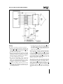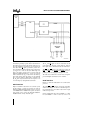
1
Microprocessor Peripherals
UPI- 41A/41AH/42/42AH
User’s Manual
October 1993
Order Number: 231318-006
Information in this document is provided in connection with Intel products. Intel assumes no liability whatsoever, including infringement of any patent or copyright, for sale and use of Intel products except as provided in
Intel’s Terms and Conditions of Sale for such products.
Intel retains the right to make changes to these specifications at any time, without notice. Microcomputer
Products may have minor variations to this specification known as errata.
*Other brands and names are the property of their respective owners.
² Since publication of documents referenced in this document, registration of the Pentium, OverDrive and
iCOMP trademarks has been issued to Intel Corporation.
Contact your local Intel sales office or your distributor to obtain the latest specifications before placing your
product order.
Copies of documents which have an ordering number and are referenced in this document, or other Intel
literature, may be obtained from:
Intel Corporation
P.O. Box 7641
Mt. Prospect, IL 60056-7641
or call 1-800-879-4683
COPYRIGHT © INTEL CORPORATION, 1996
Microprocessor Peripherals
UPI-41A/41AH/42/42AH User’s Manual
CONTENTS
PAGE
CHAPTER 1. INTRODUCTION ÀÀÀÀÀÀÀÀÀÀÀÀÀ 1
Interface Registers for Multiprocessor
Configurations ÀÀÀÀÀÀÀÀÀÀÀÀÀÀÀÀÀÀÀÀÀÀÀÀÀÀÀ 3
Powerful 8-Bit Processor ÀÀÀÀÀÀÀÀÀÀÀÀÀÀÀÀÀÀÀ 3
Special Instruction Set Features ÀÀÀÀÀÀÀÀÀÀÀÀ 4
Preprogrammed UPI’s ÀÀÀÀÀÀÀÀÀÀÀÀÀÀÀÀÀÀÀÀÀÀ 5
Development Support ÀÀÀÀÀÀÀÀÀÀÀÀÀÀÀÀÀÀÀÀÀÀ 6
UPI Development Support ÀÀÀÀÀÀÀÀÀÀÀÀÀÀÀÀÀÀ 6
CHAPTER 2. FUNCTIONAL
DESCRIPTION ÀÀÀÀÀÀÀÀÀÀÀÀÀÀÀÀÀÀÀÀÀÀÀÀÀÀ 7
Pin Description ÀÀÀÀÀÀÀÀÀÀÀÀÀÀÀÀÀÀÀÀÀÀÀÀÀÀÀÀÀ 7
CPU Section ÀÀÀÀÀÀÀÀÀÀÀÀÀÀÀÀÀÀÀÀÀÀÀÀÀÀÀÀÀÀ 10
Program Memory ÀÀÀÀÀÀÀÀÀÀÀÀÀÀÀÀÀÀÀÀÀÀÀÀÀÀ 11
Interrupt Vectors ÀÀÀÀÀÀÀÀÀÀÀÀÀÀÀÀÀÀÀÀÀÀÀÀÀÀ 11
Data Memory ÀÀÀÀÀÀÀÀÀÀÀÀÀÀÀÀÀÀÀÀÀÀÀÀÀÀÀÀÀ 11
Program Counter ÀÀÀÀÀÀÀÀÀÀÀÀÀÀÀÀÀÀÀÀÀÀÀÀÀÀ 12
Program Counter Stack ÀÀÀÀÀÀÀÀÀÀÀÀÀÀÀÀÀÀÀ 12
Program Status Word ÀÀÀÀÀÀÀÀÀÀÀÀÀÀÀÀÀÀÀÀÀ 13
Conditional Branch Logic ÀÀÀÀÀÀÀÀÀÀÀÀÀÀÀÀÀÀ 13
Oscillator and Timing Circuits ÀÀÀÀÀÀÀÀÀÀÀÀÀÀ 14
Interval Timer/Event Counter ÀÀÀÀÀÀÀÀÀÀÀÀÀÀ 16
Test Inputs ÀÀÀÀÀÀÀÀÀÀÀÀÀÀÀÀÀÀÀÀÀÀÀÀÀÀÀÀÀÀÀÀ 17
Interrupts ÀÀÀÀÀÀÀÀÀÀÀÀÀÀÀÀÀÀÀÀÀÀÀÀÀÀÀÀÀÀÀÀÀ 18
CONTENTS
PAGE
Reset ÀÀÀÀÀÀÀÀÀÀÀÀÀÀÀÀÀÀÀÀÀÀÀÀÀÀÀÀÀÀÀÀÀÀÀÀÀ 19
Data Bus Buffer ÀÀÀÀÀÀÀÀÀÀÀÀÀÀÀÀÀÀÀÀÀÀÀÀÀÀÀ 20
System Interface ÀÀÀÀÀÀÀÀÀÀÀÀÀÀÀÀÀÀÀÀÀÀÀÀÀÀ 21
Input/Output Interface ÀÀÀÀÀÀÀÀÀÀÀÀÀÀÀÀÀÀÀÀ 22
Ports 1 and 2 ÀÀÀÀÀÀÀÀÀÀÀÀÀÀÀÀÀÀÀÀÀÀÀÀÀÀÀÀÀÀ 22
Ports 4, 5, 6, and 7 ÀÀÀÀÀÀÀÀÀÀÀÀÀÀÀÀÀÀÀÀÀÀÀÀ 23
CHAPTER 3. INSTRUCTION SET ÀÀÀÀÀÀÀÀ 26
Instruction Set Description ÀÀÀÀÀÀÀÀÀÀÀÀÀÀÀÀ 28
Alphabetic Listing ÀÀÀÀÀÀÀÀÀÀÀÀÀÀÀÀÀÀÀÀÀÀÀÀÀ 30
CHAPTER 4. SINGLE-STEP AND
PROGRAMMING POWER-DOWN
MODES ÀÀÀÀÀÀÀÀÀÀÀÀÀÀÀÀÀÀÀÀÀÀÀÀÀÀÀÀÀÀÀÀ 53
Single-Step ÀÀÀÀÀÀÀÀÀÀÀÀÀÀÀÀÀÀÀÀÀÀÀÀÀÀÀÀÀÀÀ 53
External Access ÀÀÀÀÀÀÀÀÀÀÀÀÀÀÀÀÀÀÀÀÀÀÀÀÀÀÀ 55
Power Down Mode
(UPI-41AH/42AH Only) ÀÀÀÀÀÀÀÀÀÀÀÀÀÀÀÀÀ 55
CHAPTER 5. SYSTEM OPERATION ÀÀÀÀÀÀ 56
Bus Interface ÀÀÀÀÀÀÀÀÀÀÀÀÀÀÀÀÀÀÀÀÀÀÀÀÀÀÀÀÀ 56
Design Examples ÀÀÀÀÀÀÀÀÀÀÀÀÀÀÀÀÀÀÀÀÀÀÀÀÀ 57
General Handshaking Protocol ÀÀÀÀÀÀÀÀÀÀÀÀ 60
CHAPTER 6. APPLICATIONS ÀÀÀÀÀÀÀÀÀÀÀÀ 62
Abstracts ÀÀÀÀÀÀÀÀÀÀÀÀÀÀÀÀÀÀÀÀÀÀÀÀÀÀÀÀÀÀÀÀÀ 62
UPI-41A/41AH/42/42AH USER’S MANUAL
CHAPTER 1
INTRODUCTION
Accompanying the introduction of microprocessors
such as the 8088, 8086, 80186 and 80286 there has been
a rapid proliferation of intelligent peripheral devices.
These special purpose peripherals extend CPU performance and flexibility in a number of important
ways.
Table 1-1. Intelligent Peripheral Devices
8255 (GPIO)
Programmable Peripheral
Interface
8251A(USART)
Programmable
Communication Interface
8253 (TIMER)
Programmable Interval Timer
8257 (DMA)
Programmable DMA Controller
8259
Programmable Interrupt
Controller
82077AA
Programmable Floppy Disk
Controller
8273 (SDLC)
Programmable Synchronous
Data Link Controller
8274
Programmable MultiprotocolSerial Communications
Controller
8275/8276 (CRT) Programmable CRT
Controllers
8279 (PKD)
Programmable
Keyboard/Display Controller
8291A, 8292, 8293 Programmable GPIB System
Talker, Listener, Controller
Intelligent devices like the 82077AA floppy disk controller and 8273 synchronous data link controller (see
Table 1-1) can preprocess serial data and perform control tasks which off-load the main system processor.
Higher overall system throughput is achieved and software complexity is greatly reduced. The intelligent
peripheral chips simplify master processor control tasks
by performing many functions externally in peripheral
hardware rather than internally in main processor software.
Intelligent peripherals also provide system flexibility.
They contain on-chip mode registers which are programmed by the master processor during system initialization. These control registers allow the peripheral to
be configured into many different operation modes. The
user-defined program for the peripheral is stored in
main system memory and is transferred to the peripheral’s registers whenever a mode change is required. Of
course, this type of flexibility requires software overhead in the master system which tends to limit the benefit derived from the peripheral chip.
In the past, intelligent peripherals were designed to
handle very specialized tasks. Separate chips were designed for communication disciplines, parallel I/O,
keyboard encoding, interval timing, CRT control, etc.
Yet, in spite of the large number of devices available
and the increased flexibility built into these chips, there
is still a large number of microcomputer peripheral
control tasks which are not satisfied.
With the introduction of the Universal Peripheral Interface (UPI) microcomputer, Intel has taken the intelligent peripheral concept a step further by providing an
intelligent controller that is fully user programmable. It
is a complete single-chip microcomputer which can
connect directly to a master processor data bus. It has
the same advantages of intelligence and flexibility
which previous peripheral chips offered. In addition,
UPIs are user-programmable: it has 1K/2K bytes of
ROM or EPROM memory for program storage plus
64/128/256 bytes of RAM memory UPI-41A,
41AH/42, 42AH respectively for data storage or initialization from the master processor. The UPI device
allows a designer to fully specify his control algorithm
in the peripheral chip without relying on the master
processor. Devices like printer controllers and keyboard scanners can be completely self-contained, relying on the master processor only for data transfer.
The UPI family currently consists of seven components:
# 8741A microcomputer with 1K EPROM memory
# 8741AH microcomputer with 1K OTP EPROM
memory
# 8041AH microcomputer with 1K ROM memory
# 8742 microcomputer with 2K EPROM memory
# 8742AH microcomputer with 2K ‘‘OTP’’ EPROM
memory
# 8042AH microcomputer with 2K ROM memory
# 8243 I/O expander device
The UPI-41A/41AH/42/42AH family of microcomputers are functionally equivalent except for the type
and amount of program memory available with each.
In addition, the UPI-41AH/42AH family has a Signature Row outside the EPROM Array. The UPI-41AH/
42AH family also has a Security Feature which renders
the EPROM Array unreadable when set.
1
UPI-41A/41AH/42/42AH USER’S MANUAL
All UPI’s have the following main features:
# 8-bit CPU
# 8-bit data bus interface registers
# Interval timer/event counter
# Two 8-bit TTL compatible I/O ports
# Resident clock oscillator circuits
The UPI family has the following differences:
Table 1-2
UPI-41A
UPI-42
1K x 8 EPROM
2K x 8 EPROM
64 x 8 RAM
128 x 8 RAM
UPI-41AH
UPI-42AH
1K x 8 ROM
2K x 8 ROM
or 1K x 8 OTP
or
2K x 8 OTP
128 x 8 RAM
256 x 8 RAM
*Set Security Feature
**Signature Row Feature
32 Bytes with:
1. Test Code/Checksum
2. Intel Signature
3. Security Byte
4. User Signature
PROGRAMMING
UPI-41A
UPI-42
UPI-41AH/UPI-42AH
VDD e 25V
IDD e 50 ms
EA e 21.5V–24.5V
VPH e 21.5V–24.5V
TPW e 50 ms
21V
50 mA
18V
18V
50 ms
12.5V
30 mA
12.5V
20.V – 5.5V
1 ms
PIN DESCRIPTION
UPI-41A/UPI-42
UPI-41AH/UPI-42AH
(T1)
T1 functions as a test input which can be
directly tested using conditional branching
instructions. It functions as the event timer input
under software control.
T1 functions as a test input that can be directly
tested using conditional branching instructions. It
works as the event timer input under software
control. It is used during sync mode to reset the
instruction state to S1 and synchronize the
internal clock to phase 1.
(SS)
Single step input used with the sync
output to step the program through each
instruction.
Single step input used with the sync output to
step the program through each instruction.
This pin is used to put the device in sync mode by
applying a 12.5V to it.
Port 1 (P10–P17): 8-bit, Quasi-Bidirectional I/O
Lines.
Port 1 (P10 – P17): 8-bit, Quasi-Bidirectional I/O
Lines. P10 – P17 access the Signature Row and
Security Bit.
NOTES:
*For a complete description of the Security Feature, refer to the UPI-41AH/42AH Datasheet.
**For a complete description of the Signature Row, refer to the UPI-41AH/42AH Datasheet.
2
UPI-41A/41AH/42/42AH USER’S MANUAL
HMOS processing has been applied to the UPI family
to allow for additional performance and memory capability while reducing costs. The UPI-41A/41AH/42/
42AH are all pin and software compatible. This allows
growth in present designs to incorporate new features
and add additional performance. For new designs, the
additional memory and performance of the UPI41A/41AH/42/42AH extends the UPI ‘grow your
own solution’ concept to more complex motor control
tasks, 80-column printers and process control applications as examples.
The 8243 device is an I/O multiplexer which allows
expansion of I/O to over 100 lines (if seven devices are
used). All three parts are fabricated with N-channel
MOS technology and require a single, 5V supply for
operation.
INTERFACE REGISTERS FOR MULTIPROCESSOR CONFIGURATIONS
In the normal configuration, the UPI-41A/41AH/42/
42AH interfaces to the system bus, just like any intelligent peripheral device (see Figure 1-1). The host processor and the UPI-41A/41AH/42/42AH form a loosely coupled multi-processor system, that is, communications between the two processors are direct. Common
resources are three addressable registers located physically on the UPI-41A/41AH/42/42AH. These reg-
isters are the Data Bus Buffer Input (DBBIN), Data
Bus Buffer Output (DBBOUT), and Status (STATUS)
registers. The host processor may read data from
DBBOUT or write commands and data into DBBIN.
The status of DBBOUT and DBBIN plus user-defined
status is supplied in STATUS. The host may read
STATUS at any time. An interrupt to the UPI processor is automatically generated (if enabled) when
DBBIN is loaded.
Because the UPI contains a complete microcomputer
with program memory, data memory, and CPU it can
function as a ‘‘Universal’’ controller. A designer can
program the UPI to control printers, tape transports, or
multiple serial communication channels. The UPI can
also handle off-line arithmetic processing, or any number of other low speed control tasks.
POWERFUL 8-BIT PROCESSOR
The UPI contains a powerful, 8-bit CPU with as fast as
1.2 msec cycle time and two single-level interrupts. Its
instruction set includes over 90 instructions for easy
software development. Most instructions are single byte
and single cycle and none are more than two bytes long.
The instruction set is optimized for bit manipulation
and I/O operations. Special instructions are included to
allow binary or BCD arithmetic operations, table lookup routines, loop counters, and N-way branch routines.
231318 – 1
Figure 1-1. Interfacing Peripherals To Microcomputer Systems
3
UPI-41A/41AH/42/42AH USER’S MANUAL
231318 – 49
8741A
Electrically
Programmable
Light Erasable
EPROM
231318 – 47
8741AH, 8742AH
Electrically
Programmed
OTP EPROM
231318 – 2
8041AH, 8042AH
Programmed
ROM
231318 – 3
D8742
Electrically
Programmable
Light Erasable
EPROM
Figure 1-2. Pin Compatible ROM/EPROM Versions
SPECIAL INSTRUCTION SET
FEATURES
# For Loop Counters:
Decrement Register and Jump if not zero.
# For Bit Manipulation:
AND to A (immediate data or Register)
OR to A (immediate data or Register)
XOR to A (immediate data or Register)
AND to Output Ports (Accumulator)
OR to Output Ports (Accumulator)
Jump Conditionally on any bit in A
# For BDC Arithmetic:
Decimal Adjust A
Swap 4-bit Nibbles of A
Exchange lower nibbles of A and Register
Rotate A left or right with or without Carry
# For Lookup Tables:
Load A from Page of ROM (Address in A)
Load A from Current Page of ROM
(Address in A)
231318 – 5
Figure 1-3. Interfaces and Protocols for Multiprocessor Systems
4
UPI-41A/41AH/42/42AH USER’S MANUAL
Features for Peripheral Control
The UPI 8-bit interval timer/event counter can be used
to generate complex timing sequences for control applications or it can count external events such as switch
closures and position encoder pulses. Software timing
loops can be simplified or eliminated by the interval
timer. If enabled, an interrupt to the CPU will occur
when the timer overflows.
The UPI I/O complement contains two TTL-compatible 8-bit bidirectional I/O ports and two general-purpose test inputs. Each of the 16 port lines can individually function as either input or output under software
control. Four of the port lines can also function as an
interface for the 8243 I/O expander which provides
four additional 4-bit ports that are directly addressable
by UPI software. The 8243 expander allows low cost
I/O expansion for large control applications while
maintaining easy and efficient software port addressing.
The UPI program memory is available in three types to
allow flexibility in moving from design to prototype to
production with the same PC layout. The 8741A/8742
device with EPROM memory is very economical for
initial system design and development. Its program
memory can be electrically programmed using the Intel
Universal PROM Programmer. When changes are
needed, the entire program can be erased using UV
lamp and reprogrammed in about 20 minutes. This
means the 8741A/8742 can be used as a single chip
‘‘breadboard’’ for very complex interface and control
problems. After the 8741A/8742 is programmed it can
be tested in the actual production level PC board and
the actual functional environment. Changes required
during system debugging can be made in the
8741A/8742 program much more easily than they
could be made in a random logic design. The system
configuration and PC layout can remain fixed during
the development process and the turn around time between changes can be reduced to a minimum.
At any point during the development cycle, the
8741A/8742 EPROM part can be replaced with the
low cost UPI-41AH/42AH respectively with factory
mask programmed memory or OTP EPROM. The
transition from system development to mass production
is made smoothly because the 8741A/8742, 8741AH
and 8041AH, 8742AH and 8042AH parts are completely pin compatible. This feature allows extensive
testing with the EPROM part, even into initial shipments to customers. Yet, the transition to low-cost
ROMs or OTP EPROM is simplified to the point of
being merely a package substitution.
231318 – 4
Figure 1-4. 8243 I/O Expander Interface
On-Chip Memory
The UPI’s 64/128/256 bytes data memory include dual
working register banks and an 8-level program counter
stack. Switching between the register banks allows fast
response to interrupts. The stack is used to store return
addresses and processor status upon entering a subroutine.
PREPROGRAMMED UPI’s
The 8242AH, 8292, and 8294 are 8042AH’s that are
programmed by Intel and sold as standard peripherals.
Intel offers a complete line of factory programmed keyboard controllers. These devices contain firmware developed by Phoenix Technologies Ltd. and Award Software Inc. See Table 1-3 for a complete listing of Intels’
entire keyboard controller product line. The 8292 is a
GPIB controller, part of a three chip GPIB system.
The 8294 is a Data Encryption Unit that implements
the National Bureau of Standards data encryption algorithm. These parts illustrate the great flexibility offered
by the UPI family.
5
UPI-41A/41AH/42/42AH USER’S MANUAL
Table 1-3. Keyboard Controller Family Product Selection Guide
UPI-42: The industry standard for desktop Keyboard Control.
Device
Package
ROM
OTP
8042
N, P
8242
8242PC
N, P
N, P
Phoenix firmware version 2.5
Phoenix MultiKey/42 firmware, PS/2 style mouse support
8242WA
8242WB
N, P
N, P
Award firmware version 3.57
Award firmware version 4.14, PS/2 style mouse support
8742
N, P, D
2K
Comments
ROM Device
2K
Available as OTP (N, P) or EPROM (D)
UPI-C42: A low power CHMOS version of the UPI-42. The UPI-C42 doubles the user programmable memory size,
adds Auto A20 Gate support, includes Standby (**) and Suspend power down modes, and is available in a space
saving 44-lead QFP pkg.
Device
Package
80C42
N, P, S
82C42PC
82C42PD
82C42PE
N, P, S
N, P, S
N, P, S
87C42
N, P, S
ROM
OTP
4K
Comments
ROM Device
Phoenix MultiKey/42 firmware, PS/2 style mouse support
Phoenix MultiKey/42L firmware, KBC and SCC for portable apps.
Phoenix MultiKey/42G firmware, Energy Efficient KBC solution
4K
One Time Programmable Version
UPI-L42: The low voltage 3.3V version of the UPI-C42.
Device
Package
80L42
N, P, S
82L42PC
82L42PD
N, P, S
N, P, S
87L42
N, P, S
ROM
OTP
4K
Comments
ROM Device
Phoenix MultiKey/42 firmware, PS/2 style mouse support
Phoenix MultiKey/42L firmware, KBC and SCC for portable apps.
4K
One Time Programmable Version
NOTES:
N e 44 lead PLCC, P e 40 lead PDIP, S e 44 lead QFP, D e 40 lead CERDIP
KBC e Key Board Control, SCC e Scan Code Control
(**) Standby feature not supported on current (B-1) stepping
DEVELOPMENT SUPPORT
The UPI microcomputer is fully supported by Intel
with development tools like the UPP PROM programmer already mentioned. The combination of device features and Intel development support make the UPI an
ideal component for low-speed peripheral control applications.
6
UPI DEVELOPMENT SUPPORT
#
#
#
#
8048/UPI-41A/41AH/42/42AH Assembler
Universal PROM Programmer UPP Series
Application Engineers
Training Courses
UPI-41A/41AH/42/42AH USER’S MANUAL
CHAPTER 2
FUNCTIONAL DESCRIPTION
The UPI microcomputer is an intelligent peripheral
controller designed to operate in iAPX-86, 88, MCS-85,
MCS-80, MCS-51 and MCS-48 systems. The UPI’s architecture, illustrated in Figure 2-1, is based on a low
cost, single-chip microcomputer with program memory, data memory, CPU, I/O, event timer and clock oscillator in a single 40-pin package. Special interface registers are included which enable the UPI to function as
a peripheral to an 8-bit master processor.
This chapter provides a basic description of the UPI
microcomputer and its system interface registers. Unless otherwise noted the descriptions in this section apply to the 8741AH, 8742AH with OTP EPROM mem-
ory, the 8741A/8742 (with UV erasable program memory) and the 8041AH, 8042AH. These devices are so
similar that they can be considered identical under
most circumstances. All functions described in this
chapter apply to the UPI-41A/41AH/42/42AH.
PIN DESCRIPTION
The UPI-41A/41AH/42/42AH are packaged in 40-pin
Dual In-Line (DIP) packages. The pin configuration
for both devices is shown in Figure 2-2. Figure 2-3 illustrates the UPI Logic Symbol.
231318 – 6
Figure 2-1. UPI-41A/41AH/42/42AH Single Chip Microcomputer
7
UPI-41A/41AH/42/42AH USER’S MANUAL
231318 – 7
Figure 2-2. Pin Configuration
231318 – 8
Figure 2-3. Logic Symbol
8
UPI-41A/41AH/42/42AH USER’S MANUAL
The following section summarizes the functions of each UPI pin. NOTE that several pins have two or more
functions which are described in separate paragraphs.
Symbol
D0 –D7
(BUS)
Pin No.
12–19
Type
I/O
P10 –P17
P20 –P27
27-34
21-24
35–38
I/O
I/O
WR
10
I
RD
8
I
CS
6
I
A0
9
I
TEST 0,
TEST 1
1
39
I
XTAL 1,
XTAL 2
SYNC
2
3
11
I
O
EA
7
I
PROG
25
I/O
RESET
4
I
SS
5
I
VCC
VDD
40
26
VSS
20
Table 2-1. Pin Description
Name and Function
DATA BUS: Three-state, bidirectional DATA BUS BUFFER
lines used to interface the UPI-41A/41AH/42/42AH
microcomputer to an 8-bit master system data bus.
PORT 1: 8-bit, PORT 1 quasi-bidirectional I/O lines.
PORT 2: 8-bit, PORT 2 quasi-bidirectional I/O lines. The lower
4 bits (P20 –P23) interface directly to the 8243 I/O expander
device and contain address and data information during PORT
4– 7 access. The upper 4 bits (P24 –P27) can be programmed
to provide interrupt Request and DMA Handshake capability.
Software control can configure P24 as Output Buffer Full
(OBF) interrupt, P25 as Input Buffer Full (IBF) interrupt, P26 as
DMA Request (DRQ), and P27 as DMA
ACKnowledge (DACK).
WRITE: I/O write input which enables the master CPU to write
data and command words to the UPI INPUT DATA BUS
BUFFER.
READ: I/O read input which enables the master CPU to read
data and status words from the OUTPUT DATA BUS BUFFER
or status register.
CHIP SELECT: Chip select input used to select one UPI41A/41AH/42/42AH microcomputer out of several
connected to a common data bus.
COMMAND/DATA SELECT: Address input used by the
master processor to indicate whether byte transfer is data
(A0 e 0) or command (A0 e 1).
TEST INPUTS: Input pins can be directly tested using
conditional branch instructions.
FREQUENCY REFERENCE: TEST 1 (T1) also functions as
the event timer input (under software control). TEST0 (T0) is
used during PROM programming and verification in the UPI41A/41AH/42/42AH.
INPUTS: Inputs for a crystal, LC or an external timing signal to
determine the internal oscillator frequency.
OUTPUT CLOCK: Output signal which occurs once per UPI
instruction cycle. SYNC can be used as a strobe for external
circuitry; it is also used to synchronize single step operation.
EXTERNAL ACCESS: External access input which allows
emulation, testing and PROM/ROM verification.
PROGRAM: Multifunction pin used as the program pulse input
during PROM programming.
During I/O expander access the PROG pin acts as an
address/data strobe to the 8243.
RESET: Input used to reset status flip-flops and to set the
program counter to zero. RESET is also used during PROM
programming and verification.
SINGLE STEP: Single step input used in conjunction with the
SYNC output to step the program through each instruction.
POWER: a 5V main power supply pin.
POWER: a 5V during normal operation. a 25V for UPI-41A,
21V for UPI-42 programming operation, a 12V for
programming, UPI-41AH/42AH. Low power standby pin in
ROM version.
GROUND: Circuit ground potential.
9
UPI-41A/41AH/42/42AH USER’S MANUAL
The following sections provide a detailed functional description of the UPI microcomputer. Figure 2-4 illustrates the functional blocks within the UPI device.
CPU SECTION
The CPU section of the UPI-41A/41AH/42/42AH
microcomputer performs basic data manipulations and
controls data flow throughout the single chip computer
via the internal 8-bit data bus. The CPU section includes the following functional blocks shown in Figure
2-4:
#
#
#
#
Arithmetic Logic Unit (ALU)
Instruction Decoder
Accumulator
If an operation such as an ADD or ROTATE requires
more than 8 bits, the CARRY flag is used as an indicator. Likewise, during decimal adjust and other BCD
operations the AUXILIARY CARRY flag can be set
and acted upon. These flags are part of the Program
Status Word (PSW).
Instruction Decoder
Flags
Arithmetic Logic Units (ALU)
The ALU is capable of performing the following operations:
#
#
#
#
#
#
#
In a typical operation data from the accumulator is
combined in the ALU with data from some other
source on the UPI-41A/41AH/42/42AH internal bus
(such as a register or an I/O port). The result of an
ALU operation can be transferred to the internal bus or
back to the accumulator.
ADD with or without carry
During an instruction fetch, the operation code (opcode) portion of each program instruction is stored and
decoded by the instruction decoder. The decoder generates outputs used along with various timing signals to
control the functions performed in the ALU. Also, the
instruction decoder controls the source and destination
of ALU data.
AND, OR, and EXCLUSIVE OR
Increment, Decrement
Accumulator
Bit complement
Rotate left or right
Swap
The accumulator is the single most important register
in the processor. It is the primary source of data to the
ALU and is often the destination for results as well.
Data to and from the I/O ports and memory normally
passes through the accumulator.
BCD decimal adjust
231318 – 9
Figure 2-4. UPI-41A/41AH/42/42AH Block Diagram
10
UPI-41A/41AH/42/42AH USER’S MANUAL
PROGRAM MEMORY
INTERRUPT VECTORS
The UPI-41A/41AH/42/42AH microcomputer has
1024, 2048 8-bit words of resident, read-only memory
for program storage. Each of these memory locations is
directly addressable by a 10-bit program counter. Depending on the type of application and the number of
program changes anticipated, three types of program
memory are available:
1) Location 0
Following a RESET input to the processor, the next
instruction is automatically fetched from location 0.
# 8041AH, 8042AH with mask programmed ROM
Memory
# 8741AH, 8742AH with electrically programmable
OTP EPROM Memory
# 8741A and 8742 with electrically programmable
EPROM Memory
A program memory map is illustrated in Figure 2-5.
Memory is divided into 256 location ‘pages’ and three
locations are reserved for special use:
2) Location 3
An interrupt generated by an Input Buffer Full
(IBF) condition (when the IBF interrupt is enabled)
causes the next instruction to be fetched from location 3.
3) Location 7
A timer overflow interrupt (when enabled) will
cause the next instruction to be fetched from location 7.
Following a system RESET, program execution begins
at location 0. Instructions in program memory are normally executed sequentially. Program control can be
transferred out of the main line of code by an input
buffer full (IBF) interrupt or a timer interrupt, or when
a jump or call instruction is encountered. An IBF interrupt (if enabled) will automatically transfer control to
location 3 while a timer interrupt will transfer control
to location 7.
All conditional JUMP instructions and the indirect
JUMP instruction are limited in range to the current
256-location page (that is, they alter PC bits 0 – 7 only).
If a conditional JUMP or indirect JUMP begins in location 255 of a page, it must reference a destination on
the following page.
Program memory can be used to store constants as well
as program instructions. The UPI-41AH, 42AH instruction set contains an instruction (MOVP3) designed specifically for efficient transfer of look-up table
information from page 3 of memory.
DATA MEMORY
231318 – 10
Figure 2-5. Program Memory Map
The UPI-41A has 64 8-bit words of Random Access
Memory, the UPI-41AH has 128 8-bit words of Random Access Memory; the UPI-42 has 128 8-bit words
of RAM; and the UPI-42AH has 256 8-bit words of
RAM. This memory contains two working register
banks, an 8-level program counter stack and a scratch
pad memory, as shown in Figure 2-6. The amount of
scratch pad memory available is variable depending on
the number of addresses nested in the stack and the
number of working registers being used.
Addressing Data Memory
The first eight locations in RAM are designated as
working registers R0 –R7. These locations (or registers)
can be addressed directly by specifying a register number in the instruction. Since these locations are easily
addressed, they are generally used to store frequently
11
UPI-41A/41AH/42/42AH USER’S MANUAL
accessed intermediate results. Other locations in data
memory are addressed indirectly by using R0 or R1 to
specify the desired address.
interrupt processing, registers in bank 0 can be accessed
indirectly using R0Ê and R1Ê .
If register bank 1 is not used, registers 24 – 31 can still
serve as additional scratch pad memory.
Program Counter Stack
RAM locations 8 – 23 are used as an 8-level program
counter stack. When program control is temporarily
passed from the main program to a subroutine or interrupt service routine, the 10-bit program counter and
bits 4 – 7 of the program status word (PSW) are stored
in two stack locations. When control is returned to the
main program via an RETR instruction, the program
counter and PSW bits 4 – 7 are restored. Returning via
an RET instruction does not restore the PSW bits,
however. The program counter stack is addressed by
three stack pointer bits in the PSW (bits 0 – 2). Operation of the program counter stack and the program
status word is explained in detail in the following sections.
The stack allows up to eight levels of subroutine ‘nesting’; that is, a subroutine may call a second subroutine,
which may call a third, etc., up to eight levels. Unused
stack locations can be used as scratch pad memory.
Each unused level of subroutine nesting provides two
additional RAM locations for general use.
231318 – 11
The following sections provide a detailed description of
the Program Counter Stack and the Program Status
Word.
Figure 2-6. Data Memory Map
PROGRAM COUNTER
Working Registers
Dual banks of eight working registers are included in
the UPI-41A/41AH/42/42AH data memory. Locations 0–7 make up register bank 0 and locations 24 – 13
form register bank 1. A RESET signal automatically
selects register bank 0. When bank 0 is selected, references to R0 –R7 in UPI-41A/41AH/42/42AH instructions operate on locations 0–7 in data memory. A ‘‘select register bank’’ instruction is used to selected between the banks during program execution. If the instruction SEL RB1 (Select Register Bank 1) is executed, then program references to R0 –R7 will operate on
locations 24–31. As stated previously, registers 0 and 1
in the active register bank are used as indirect address
registers for all locations in data memory.
Register bank 1 is normally reserved for handling interrupt service routines, thereby preserving the contents of
the main program registers. The SEL RB1 instruction
can be issued at the beginning of an interrupt service
routine. Then, upon return to the main program, an
RETR (return & restore status) instruction will automatically restore the previously selected bank. During
12
The UPI-41A/41AH/42/42AH microcomputer has a
10-bit program counter (PC) which can directly address any of the 1024, 2048, or 4096 locations in program memory. The program counter always contains
the address of the next instruction to be executed and is
normally incremented sequentially for each instruction
to be executed when each instruction fetches occurs.
When control is temporarily passed from the main program to a subroutine or an interrupt routine, however,
the PC contents must be altered to point to the address
of the desired routine. The stack is used to save the
current PC contents so that, at the end of the routine,
main program execution can continue. The program
counter is initialized to zero by a RESET signal.
PROGRAM COUNTER STACK
The Program Counter Stack is composed of 16 locations in Data Memory as illustrated in Figure 2-7.
These RAM locations (8 through 23) are used to store
the 10-bit program counter and 4 bits of the program
status word.
UPI-41A/41AH/42/42AH USER’S MANUAL
An interrupt or Call to a subroutine causes the contents
of the program counter to be stored in one of the 8
register pairs of the program counter stack.
DATA
MEMORY
LOCATION
STACK
POINTER
#
#
#
#
CY Ð Carry
AC Ð Auxiliary Carry
F0 Ð Flag 0
BS Ð Register Bank Select
23
111
22
21
110
20
19
101
231318 – 12
18
17
100
16
15
011
14
13
010
12
11
001
10
000
PSW(4–7)
PC(8–9)
9
PC(4–7)
PC(0–3)
8
MSB
LSB
Figure 2-7. Program Counter Stack
A 3-bit Stack Pointer which is part of the Program
Status Word (PSW) determines the stack pair to be
used at a given time. The stack pointer is initialized by
a RESET signal to 00H which corresponds to RAM
locations 8 and 9.
The first call or interrupt results in the program counter and PSW contents being transferred to RAM locations 8 and 9 in the format shown in Figure 2-7. The
stack pointer is automatically incremented by 1 to point
to location is 10 and 11 in anticipation of another
CALL.
Nesting of subroutines within subroutines can continue
up to 8 levels without overflowing the stack. If overflow
does occur the deepest address stored (locations 8 and
9) will be overwritten and lost since the stack pointer
overflows from 07H to 00H. Likewise, the stack pointer
will underflow from 00H to 07H.
The end of a subroutine is signaled by a return instruction, either RET or RETR. Each instruction will automatically decrement the Stack Pointer and transfer the
contents of the proper RAM register pair to the Program Counter.
PROGRAM STATUS WORD
The 8-bit program status word illustrated in Figure 2-8
is used to store general information about program execution. In addition to the 3-bit Stack Pointer discussed
previously, the PSW includes the following flags:
Figure 2-8. Program Status Word
The Program Status Word (PSW) is actually a collection of flip-flops located throughout the machine which
are read or written as a whole. The PSW can be loaded
to or from the accumulator by the MOV A, PSW or
MOV PSW, A instructions. The ability to write directly
to the PSW allows easy restoration of machine status
after a power-down sequence.
The upper 4 bits of the PSW (bits 4, 5, 6, and 7) are
stored in the PC Stack with every subroutine CALL or
interrupt vector. Restoring the bits on a return is optional. The bits are restored if an RETR instruction is
executed, but not if an RET is executed.
PSW bit definitions are as follows:
# Bits 0 – 2 Stack Pointer Bits S0, S1, S2
# Bit 3 Not Used
# Bit 4 Working Register Bank
0 e Bank 0
1 e Bank 1
# Bit 5 Flag 0 bit (F0)
This is a general purpose flag which can be cleared
or complemented and tested with conditional jump
instructions. It may be used during data transfer to
an external processor.
# Bit 6 Auxiliary Carry (AC)
The flag status is determined by an ADD instruction and is used by the Decimal Adjustment instruction DAA
# Bit 7 Carry (CY)
The flag indicates that a previous operation resulted
in overflow of the accumulator.
CONDITIONAL BRANCH LOGIC
Conditional Branch Logic in the UPI-41AH, 42AH allows the status of various processor flags, inputs, and
other hardware functions to directly affect program execution. The status is sampled in state 3 of the first
cycle.
13
UPI-41A/41AH/42/42AH USER’S MANUAL
Table 2-2 lists the internal conditions which are testable
and indicates the condition which will cause a jump. In
all cases, the destination address must be within the
page of program memory (256 locations) in which the
jump instruction occurs.
which UPI is used. Refer to Table 1.1. Pins XTAL 1
and XTAL 2 are input and output (respectively) of a
high gain amplifier stage. A crystal or inductor and
capacitor connected between XTAL 1 and XTAL 2
provide the feedback and proper phase shift for oscillation. Recommended connections for crystal or L-C are
shown in Figure 2-11.
OSCILLATOR AND TIMING CIRCUITS
The UPI-41A/41AH/42/42AH’s internal timing generation is controlled by a self-contained oscillator and
timing circuit. A choice of crystal, L-C or external
clock can be used to derive the basic oscillator frequency.
State Counter
The resident timing circuit consists of an oscillator, a
state counter and a cycle counter as illustrated in Figure 2-9. Figure 2-10 shows instruction cycle timing.
Each instruction cycle consists of five states as illustrated in Figure 2-10 and Table 2-3. The overlap of address
and execution operations illustrated in Figure 2-10 allows fast instruction execution.
The output of the oscillator is divided by 3 in the state
counter to generate a signal which defines the state
times of the machine.
Oscillator
The on-board oscillator is a series resonant circuit with
a frequency range of 1 to 12.5 MHz depending on
Table 2-2. Conditional Branch Instructions
Device
Instruction Mnemonic
Accumulator
JZ
JNZ
JBb
JC
JNC
JFO
JF1
JTF
JT0
JNT0
JT1
JNT1
JNIBF
JOBF
Accumulator bit
Carry flag
User flag
Timer flag
Test Input 0
Test Input 1
Input Buffer flag
Output Buffer flag
addr
addr
addr
addr
addr
addr
addr
addr
addr
addr
addr
addr
addr
addr
Jump Condition
Jump if:
All bits zero
Any bit not zero
Bit ‘‘b’’ e 1
Carry flag e 1
Carry flag e 0
F0 flag e 1
F1 flag e 1
Timer flag e 1
T0 e 1
T0 e 0
T1 e 1
T1 e 0
IBF flag e 0
OBF flag e 1
231318 – 14
231318 – 13
Figure 2-9. Oscillator Configuration
14
Figure 2-10. Instruction Cycle Timing
UPI-41A/41AH/42/42AH USER’S MANUAL
Table 2-3. Instruction Timing Diagram
CYCLE 1
Instruction
S1
S2
CYCLE 2
S3
S4
S5
S1
Ð
IN A,Pp
Fetch
Increment
Instruction Program Counter
Ð
Increment
Timer
Ð
OUTL Pp,A
Fetch
Increment
Instruction Program Counter
Ð
Increment
Timer
Output
To Port
Ð
Increment
Timer
Read Port
Fetch
Immediate
Data
Ð
Increment
Timer
Read Port
Fetch
Immediate
Data
Fetch
ANL Pp, DATA Instruction
Increment
Program
Counter
Fetch
ORL Pp, DATA Instruction
Increment
Program
Counter
MOVD A,Pp
Fetch
Increment
Output
Instruction Program Counter Opcode/Address
Increment
Timer
Ð
MOVD Pp, A
Fetch
Increment
Output
Instruction Program Counter Opcode/Address
Increment
Timer
D Pp, A
Fetch
Increment
Output
Instruction Program Counter Opcode/Address
ORLD Pp, A
Fetch
Increment
Output
Instruction Program Counter Opcode/Address
Fetch
Increment
J (Conditional) Instruction Program Counter
Ð
Ð
Ð
S4
S5
Ð
Ð
Ð
Ð
Ð
Ð
Increment Output
Ð
Program To Port
Counter
Increment Output
Ð
Program To Port
Counter
Read
P2 Lower
Ð
Ð
Ð
Output Data
To P2 Lower
Ð
Ð
Ð
Ð
Ð
Increment
Timer
Output
Data
Ð
Ð
Ð
Ð
Ð
Increment
Timer
Output
Data
Ð
Ð
Ð
Ð
Ð
Fetch
Immediate Data
Ð
Ð
Sample
Condition
Increment
Timer
Ð
Fetch
Increment
Instruction Program Counter
Ð
Increment
Timer
Update
Status Register
IN A, DBB
Fetch
Increment
Instruction Program Counter
Ð
Increment
Timer
Ð
OUT DBB, A
Fetch
Increment
Instruction Program Counter
Ð
Increment
Timer
Output
To Port
STRT T
STRT CNT
Fetch
Increment
Instruction Program Counter
Ð
Ð
Start
Counter
STOP TCNT
Fetch
Increment
Instruction Program Counter
Ð
Ð
Stop
Counter
EN I
Fetch
Increment
Instruction Program Counter
Ð
Enable
Interrupt
Ð
DIS I
Fetch
Increment
Instruction Program Counter
Ð
Disable
Interrupt
Ð
Fetch
Increment
Instruction Program Counter
Ð
DMA Enabled
DRQ Cleared
Ð
Fetch
Increment
Instruction Program Counter
Ð
OBF, IBF
Output Enabled
Ð
EN FLAGS
Ð
S3
Ð
MOV STS, A
EN DMA
S2
Read Port
Ð
Update
Program
Counter
231318 – 48
231318 – 15
Figure 2-11. Recommended Crystal and L-C Connections
15
UPI-41A/41AH/42/42AH USER’S MANUAL
Cycle Counter
INTERVAL TIMER/EVENT COUNTER
The output of the state counter is divided by 5 in the
cycle counter to generate a signal which defines a machine cycle. This signal is call SYNC and is available
continuously on the SYNC output pin. It can be used
to synchronize external circuitry or as a general purpose clock output. It is also used for synchronizing single-step.
The UPI-41A/41AH/42/42AH has a resident 8-bit
timer/counter which has several software selectable
modes of operation. As an interval timer, it can generate accurate delays from 80 microseconds to 20.48 milliseconds without placing undue burden on the processor. In the counter mode, external events such as switch
closures or tachometer pulses can be counted and used
to direct program flow.
Frequency Reference
Timer Configuration
The external crystal provides high speed and accurate
timing generation. A crystal frequency of 5.9904 MHz
is useful for generation of standard communication frequencies by the UPI-41A/41AH/42/42AH. However,
if an accurate frequency reference and maximum processor speed are not required, an inductor and capacitor
may be used in place of the crystal as shown in Figure
2-11.
A recommended range of inductance and capacitance
combinations is given below:
# L e 130 mH corresponds to 3 MHz
# L e 45 mH corresponds to 5 MHz
An external clock signal can also be used as a frequency
reference to the UPI-41A/41AH/42/42AH; however,
the levels are not TTL compatible. The signal must be
in the 1–12.5 MHz frequency range depending on
which UPI is used. Refer to Table 1-2. The signal must
be connected to pins XTAL 1 and XTAL 2 by buffers
with a suitable pull-up resistor to guarantee that a logic
‘‘1’’ is above 3.8 volts. The recommended connection is
shown in Figure 2-12.
Figure 2-13 illustrates the basic timer/counter configuration. An 8-bit register is used to count pulses from
either the internal clock and prescaler or from an external source. The counter is presettable and readable with
two MOV instructions which transfer the contents of
the accumulator to the counter and vice-versa (i.e.
MOV T, A and MOV A, T). The counter is stopped by
a RESET or STOP TCNT instruction and remains
stopped until restarted either as a timer (START T instruction) or as a counter (START CNT instruction).
Once started, the counter will increment to its maximum count (FFH) and overflow to zero continuing its
count until stopped by a STOP TCNT instruction or
RESET.
The increment from maximum count to zero (overflow)
results in setting the Timer Flag (TF) and generating an
interrupt request. The state of the overflow flag is testable with the conditional jump instruction, JTF. The
flag is reset by executing a JTF or by a RESET signal.
The timer interrupt request is stored in a latch and
ORed with the input buffer full interrupt request. The
timer interrupt can be enabled or disabled independent
of the IBF interrupt by the EN TCNTI and DIS
TCTNI instructions. If enabled, the counter overflow
will cause a subroutine call to location 7 where the timer service routine is stored. If the timer and Input Buffer Full interrupts occur simultaneously, the IBF source
will be recognized and the call will be to location 3.
Since the timer interrupt is latched, it will remain pending until the DBBIN register has been serviced and will
immediately be recognized upon return from the service routine. A pending timer interrupt is reset by the
initiation of a timer interrupt service routine.
Event Counter Mode
231318 – 16
Figure 2-12. Recommended Connection
For External Clock Signal
16
The STRT CNT instruction connects the TEST 1 input
pin to the counter input and enables the counter. Note
this instruction does not clear the counter. The counter
is incremented on high to low transitions of the TEST 1
input. The TEST 1 input must remain high for a minimum of one state in order to be registered (250 ns at
12 MHz). The maximum count frequency is one count
per three instruction cycles (267 kHz at 12 MHz).
There is no minimum frequency limit.
UPI-41A/41AH/42/42AH USER’S MANUAL
Timer Mode
The STRT T instruction connects the internal clock to
the counter input and enables the counter. The input
clock is derived from the SYNC signal of the internal
oscillator and the divide-by-32 prescaler. The configuration is illustrated in Figure 2-13. Note this instruction
does not clear the timer register. Various delays and
timing sequences between 40 msec and 10.24 msec can
easily be generated with a minimum of software timing
loops (at 12 MHz).
Times longer than 10.24 msec can be accurately measured by accumulating multiple overflows in a register
under software control. For time resolution less than 40
msec, an external clock can be applied to the TEST 1
counter input (see Event Counter Mode). The minimum time resolution with an external clock is 3.75
msec (267 kHz at 12 MHz).
TEST 1 Event Counter Input
The TEST 1 pin is multifunctional. It is automatically
initialized as a test input by a RESET signal and can be
tested using UPI-41A conditional branch instructions.
In the second mode of operation, illustrated in Figure
2-13, the TEST 1 pin is used as an input to the internal
8-bit event counter. The Start Counter (STRT CNT)
instruction controls an internal switch which connects
TEST 1 through an edge detector to the 8-bit internal
counter. Note that this instruction does not inhibit the
testing of TEST 1 via conditional Jump instructions.
In the counter mode the TEST 1 input is sampled once
per instruction cycle. After a high level is detected, the
next occurrence of a low level at TEST 1 will cause the
counter to increment by one.
The event counter functions can be stopped by the Stop
Timer/Counter (STOP TCNT) instruction. When this
instruction is executed the TEST 1 pin becomes a test
input and functions as previously described.
TEST INPUTS
There are two multifunction pins designated as Test
Inputs, TEST 0 and TEST 1. In the normal mode of
operation, status of each of these lines can be directly
tested using the following conditional Jump instructions:
#
#
#
#
JT0
JNT0
JT1
JNT1
Jump
Jump
Jump
Jump
if
if
if
if
TEST
TEST
TEST
TEST
0
0
1
1
e 1
e 0
e 1
e 0
231318 – 17
Figure 2-13. Timer Counter
17
UPI-41A/41AH/42/42AH USER’S MANUAL
The test imputs are TTL compatible. An external logic
signal connected to one of the test inputs will be sampled at the time the appropriate conditional jump instruction is executed. The path of program execution
will be altered depending on the state of the external
signal when sampled.
Figure 2-14 illustrates the internal interrupt logic. An
IBF interrupt request is generated whenever WR and
CS are both low, regardless of whether interrupts are
enabled. The interrupt request is cleared upon entering
the IBF service routine only. That is, the DIS I instruction does not clear a pending IBF interrupt.
INTERRUPTS
Interrupt Timing Latency
The UPI-41A/41AH/42/42AH has the following internal interrupts:
# Input Buffer Full (IBF) interrupt
When the IBF interrupt is enabled and an IBF interrupt request occurs, an interrupt sequence is intiated as
soon as the currently executing instruction is completed. The following sequence occurs:
# Timer Overflow interrupt
The IBF interrupt forces a CALL to location 3 in program memory; a timer-overflow interrupts forces a
CALL to location 7. The IBF interrupt is enabled by
the EN I instruction and disabled by the DIS I instruction. The timer-overflow interrupt is enabled and disabled by the EN TNCTI and DIS TCNTI instructions,
respectively.
# A CALL to location 3 is forced.
# The program counter and bits 4 – 7 of the Program
Status Word are stored in the stack.
# The stack pointer is incremented.
231318 – 19
Figure 2-14. Interrupt Logic
18
UPI-41A/41AH/42/42AH USER’S MANUAL
Location 3 in program memory should contain an unconditional jump to the beginning of the IBF interrupt
service routine elsewhere in program memory. At the
end of the service routine, an RETR (Return and Restore Status) instruction is used to return control to the
main program. This instruction will restore the program counter and PSW bits 4–7, providing automatic
restoration of the previously active register bank as
well. RETR also re-enables interrupts.
A timer-overflow interrupt is enabled by the EN
TCNTI instruction and disabled by the DIS TCNTI
instruction. If enabled, this interrupt occurs when the
timer/counter register overflows. A CALL to location
7 is forced and the interrupt routine proceeds as described above.
The interrupt service latency is the sum of current instruction time, interrupt recognition time, and the internal call to the interrupt vector address. The worst
case latency time for servicing an interrupt is 7 clock
cycles. Best case latency is 4 clock cycles.
Interrupt Timing
sition of the TEST 1 input pin. Also, if an IBF interrupt
occurs during servicing of the timer/counter interrupt,
it will remain pending until the end of the service routine.
Host Interrupts And DMA
If needed, two external interrupts to the host system
can be created using the EN FLAGS instruction. This
instruction allocates two I/O lines on PORT 2 (P24 and
P25). P24 is the Output Buffer Full interrupt request
line to the host system; P25 is the Input Buffer empty
interrupt request line. These interrupt outputs reflect
the internal status of the OBF flag and the IBF inverted
flag. Note, these outputs may be inhibited by writing a
‘‘0’’ to these pins. Reenabling interrupts is done by
writing a ‘‘1’’ to these port pins. Interrupts are typically
enabled after power on since the I/O ports are set in a
‘‘1’’ condition. The EN FLAG’s effect is only cancelled
by a device RESET.
DMA handshaking controls are available from two
pins on PORT 2 of the UPI-41A/41AH/42/42AH microcomputer. These lines (P26 and P27) are enabled by
the EN DMA instruction. P26 becomes DMA request
(DRQ) and P27 becomes DMA acknowledge (DACK).
The UPI program initiates a DMA request by writing a
‘‘1’’ to P26. The DMA controller transfers the data into
the DBBIN data register using DACK which acts as a
chip select. The EN DMA instruction can only be cancelled by a chip RESET.
Interrupt inputs may be enabled or disabled under program control using EN I, DIS I, EN TCNTI and DIS
TCNTI instructions. Also, a RESET input will disable
interrupts. An interrupt request must be removed before the RETR instruction is executed to return from
the service routine, otherwise the processor will re-enter the service routine immediately. Thus, the WR and
CS inputs should not be held low longer than the duration of the interrupt service routine.
RESET
The interrupt system is single level. Once an interrupt
is detected, all further interrupt requests are latched but
are not acted upon until execution of an RETR instruction re-enables the interrupt input logic. This occurs at
the beginning of the second cycle of the RETR instruction. If an IBF interrupt and a timer-overflow interrupt
occur simultaneously, the IBF interrupt will be recognized first and the timer-overflow interrupt will remain
pending until the end of the interrupt service routine.
The RESET input provides a means for internal initialization of the processor. An automatic initialization
pulse can be generated at power-on by simply connecting a 1 mfd capacitor between the RESET input and
ground as shown in Figure 2-15. It has an internal
pull-up resistor to charge the capacitor and a Schmitttrigger circuit to generate a clean transition. A 2-stage
synchronizer has been added to support reliable operation up to 12.5 MHz.
External Interrupts
An external interrupt can be created using the UPI41A/41AH/42/42AH timer/counter in the event
counter mode. The counter is first preset to FFH and
the EN TCNTI instruction is executed. A timer-overflow interrupt is generated by the first high to low tran-
If automatic initialization is used, RESET should be
held low for at least 10 milliseconds to allow the power
supply to stabilize. If an external RESET signal is used,
RESET may be held low for a minimum of 8 instruction cycles. Figure 2-15 illustrates a configuration using
an external TTL gate to generate the RESET input.
This configuration can be used to derive the RESET
signal from the 8224 clock generator in an 8080 system.
19
UPI-41A/41AH/42/42AH USER’S MANUAL
231318 – 20
Figure 2-15. External Reset Configuration
The RESET input performs the following functions:
#
#
#
#
#
#
#
#
Disables Interrupts
Clears Program Counter to Zero
Clears Stack Pointer
Clears Status Register and Flags
Clears Timer and Timer Flag
Stops Timer
Selects Register Bank 0
Sets PORTS 1 and 2 to Input Mode
DATA BUS BUFFER
Two 8-bit data bus buffer registers, DBBIN and
DBBOUT, serve as temporary buffers for commands
and data flowing between it and the master processor.
Externally, data is transmitted or received by the DBB
registers upon execution of an INput or OUTput instruction by the master processor. Four control signals
are used:
#
#
#
#
A0
Address input signifying control or data
CS Chip Select
RD Read Strobe
WR Write Strobe
Transfer can be implemented with or without UPI program interference by enabling or disabling an internal
UPI interrupt. Internally, data transfer between the
DBB and the UPI accumulator is under software con-
20
trol and is completely asynchronous to the external
processor timing. This allows the UPI software to handle peripheral control tasks independent of the main
processor while still maintaining a data interface with
the master system.
Configuration
Figure 2-16 illustrates the internal configuration of the
DBB registers. Data is stored in two 8-bit buffer registers, DBBIN and DBBOUT. DBBIN and DBBOUT
may be accessed by the external processor using the
WR line and the RD line, respectively. The data bus is
a bidirectional, three-state bus which can be connected
directly to an 8-bit microprocessor system. Four control lines (WR, RD, CS, A0) are used by the external
processor to transfer data to and from the DBBIN and
DBBOUT registers.
An 8-bit register containing status flags is used to indicate the status of the DBB registers. The eight status
flags are defined as follows:
# OBF Output Buffer Full
This flag is automatically set when the UPI-Microcomputer loads the DBBOUT register and is cleared
when the master processor reads the data register.
# IBF Input Buffer Full
This flag is set when the master processor writes a
character to the DBBIN register and is cleared
when the UPI INputs the data register contents to
its accumulator.
UPI-41A/41AH/42/42AH USER’S MANUAL
UPI Bus Contents During Status Read
ST7
ST6
ST5
ST4
F1
F0
IBF
0BF
D7
D6
D5
D4
D3
D2
D1
D0
231318 – 21
Figure 2-16. Data Bus Buffer Configuration
# F0
This is a general purpose flag which can be cleared
or toggled under UPI software control. The flag is
used to transfer UPI status information to the master processor.
# F1 Command/Data
This flag is set to the condition of the A0 input line
when the master processor writes a character to the
data register. The F1 flag can also be cleared or toggled under UPI-Microcomputer program control.
# ST4 through ST7
These bits are user defined status bits. They are defined by the MOV STS,A instruction.
SYSTEM INTERFACE
Figure 2-17 illustrates how a UPI-Microcomputer can
be connected to a standard 8080-type bus system. Data
lines D0 –D7 form a three-state, bidirectional port
which can be connected directly to the system data bus.
The UPI bus interface has sufficient drive capability
(400 mA) for small systems, however, a larger system
may require buffers.
Four control signals are required to handle the data
and status information transfer:
# WR
I/O WRITE signal used to transfer data from the
system bus to the UPI DBBIN register and set the
F1 flag in the status register.
# RD
I/O READ signal used to transfer data from the
DBBOUT register or status register to the system
data bus.
# CS
CHIP SELECT signal used to enable one 8041AH
out of several connected to a common bus.
# A0
Address input used to select either the 8-bit status
register or DBBOUT register during an I/O READ.
Also, the signal is used to set the F1 flag in the
status register during an I/O WRITE.
The WR and RD signals are active low and are standard MCS-80 peripheral control signals used to synchronize data transfer between the system bus and peripheral devices.
The CS and A0 signals are decoded from the address
bus of the master system. In a system with few I/O
devices a linear addressing configuration can be used
where A0 and A1 lines are connected directly to A0 and
CS inputs (see Figure 2-17).
Data Read
Table 2-4 illustrates the relative timing of a DBBOUT
Read. When CS, A0, and RD are low, the contents of
the DBBOUT register is placed on the three-state Data
lines D0 –D7 and the OBF flag is cleared.
The master processor uses CS, A0, WR, and RD to
control data transfer between the DBBOUT register
and the master system. The following operations are
under master processor control:
21
UPI-41A/41AH/42/42AH USER’S MANUAL
231318 – 22
Figure 2-17. Interface to 8080 System Bus
Table 2-4. Data Transfer Controls
CS RD WR A0
0
0
0
0
1
0
0
1
1
x
1
1
0
0
x
0
1
0
1
x
Read DBBOUT register
Read STATUS register
Write DBBIN data register
Write DBBIN command register
Disable DBB
Command Write
During any write (Table 2-4), the state of the A0 input
is latched into the status register in the F1 (command/
data) flag location. This additional bit is used to signal
whether DBBIN contents are command (A0 e 1) or
data (A0 e 0) information.
INPUT/OUTPUT INTERFACE
Status Read
Table 2-4 shows the logic sequence required for a
STATUS register read. When CS and RD are low with
A0 high, the contents of the 8-bit status register appears
on Data lines D0 –D7.
Data Write
Table 2-4 shows the sequence for writing information
to the DBBIN register. When CS and WR are low, the
contents of the system data bus is latched into DBBIN.
Also, the IBF flag is set and an interrupt is generated, if
enabled.
22
The UPI-41A/41AH/42/42AH has 16 lines for input
and output functions. These I/O lines are grouped as
two 8-bit TTL compatible ports: PORTS 1 and 2. The
port lines can individually function as either inputs or
outputs under software control. In addition, the lower 4
lines of PORT 2 can be used to interface to an 8243 I/O
expander device to increase I/O capacity to 28 or more
lines. The additional lines are grouped as 4-bit ports:
PORTS 4, 5, 6, and 7.
PORTS 1 and 2
PORTS 1 and 2 are each 8 bits wide and have the same
I/O characteristics. Data written to these ports by an
UPI-41A/41AH/42/42AH USER’S MANUAL
OUTL Pp,A instruction is latched and remains unchanged until it is rewritten. Input data is sampled at
the time the IN, A, Pp instruction is executed. Therefore, input data must be present at the PORT until read
by an INput instruction. PORT 1 and 2 inputs are fully
TTL compatible and outputs will drive one standard
TTL load.
Circuit Configuration
The PORT 1 and 2 lines have a special output structure
(shown in Figure 2-18) that allows each line to serve as
an input, an output, or both, even though outputs are
statically latched.
Each line has a permanent high impedance pull-up (50
KX) which is sufficient to provide source current for a
TTL high level, yet can be pulled low by a standard
TTL gate drive. Whenever a ‘‘1’’ is written to a line, a
low impedance pull-up (250X) is switched in momentarily (500 ns) to provide a fast transition from 0 to 1.
When a ‘‘0’’ is written to the line, a low impedance
pull-down (300X) is active to provide TTL current
sinking capability.
To use a particular PORT pin as an input, a logic ‘‘1’’
must first be written to that pin.
NOTE:
A RESET initializes all PORT pins to the high impedance logic ‘‘1’’ state.
An external TTL device connected to the pin has sufficient current sinking capability to pull-down the pin to
the low state. An IN A, Pp instruction will sample the
status of PORT pin and will input the proper logic
level. With no external input connected, the IN A,Pp
instruction inputs the previous output status.
This structure allows input and output information on
the same pin and also allows any mix of input and
output lines on the same port. However, when inputs
and outputs are mixed on one PORT, a PORT write
will cause the strong internal pull-ups to turn on at all
inputs. If a switch or other low impedance device is
connected to an input, a PORT write (‘‘1’’ to an input)
could cause current limits on internal lines to be exceeded. Figure 2-19 illustrates the recommended connection when inputs and outputs are mixed on one
PORT.
The bidirectional port structure in combination with
the UPI-41A/41AH/42/42AH logical AND and OR
instructions provide an efficient means for handling single line inputs and outputs within an 8-bit processor.
PORTS 4, 5, 6, and 7
By using an 8243 I/O expander, 16 additional I/O lines
can be connected to the UPI-41AH, 42AH and directly
addressed as 4-bit I/O ports using UPI-41AH, 42AH
231318 – 23
Figure 2-18. Quasi-Bidirectional Port Structure
23
UPI-41A/41AH/42/42AH USER’S MANUAL
instructions. This feature saves program space and design time, and improves the bit handling capability of
the UPI-41A/41AH/42/42AH.
The lower half of PORT 2 provides an interface to the
8243 as illustrated in Figure 2-20. The PROG pin is
used as a strobe to clock address and data information
via the PORT 2 interface. The extra 16 I/O lines are
referred to in UPI software as PORTS 4, 5, 6, and 7.
Each PORT can be directly addressed and can be
ANDed and ORed with an immediate data mask. Data
can be moved directly to the accumulator from the expander PORTS (or vice-versa).
Multiple 8243’s can be connected to the PORT 2 interface. In normal operation, only one of the 8243’s would
be active at the time an Input or Output command is
executed. The upper half of PORT 2 is used to provide
chip select signals to the 8043’s. Figure 2-21 shows how
four 8243’s could be connected. Software is needed to
select and set the proper PORT 2 pin before an INPUT
or OUTPUT command to PORTS 4 – 7 is executed. In
general, the software overhead required is very minor
compared to the added flexibility of having a large
number of I/O pins available.
The 8243 I/O ports, PORTS 4, 5, 6, and 7, provide
more drive capability than the UPI-41A/41AH/42/
42AH bidirectional ports. The 8243 output is capable
of driving about 5 standard TTL loads.
231318 – 24
Figure 2-19. Recommended PORT Input Connections
24
UPI-41A/41AH/42/42AH USER’S MANUAL
231318 – 25
231318 – 26
Figure 2-20. 8243 Expander Interface
231318 – 27
Figure 2-21. Multiple 8243 Expansion
25
UPI-41A/41AH/42/42AH USER’S MANUAL
CHAPTER 3
INSTRUCTION SET
The UPI-41A/41AH/42/42AH Instruction Set is opcode-compatible with the MCS-48 set except for the
elimination of external program and data memory instructions and the addition of the data bus buffer instructions. It is very straightforward and efficient in its
use of program memory. All instructions are either 1 or
2 bytes in length (over 70% are only 1 byte long) and
over half of the instructions execute in one machine
cycle. The remainder require only two cycles and include Branch, Immediate, and I/O operations.
The UPI-41A/41AH/42/42AH Instruction Set efficiently handles the single-bit operations required in
control applications. Special instructions allow port bits
to be set or cleared individually. Also, any accumulator
bit can be directly tested via conditional branch instructions. Additional instructions are included to simplify
loop counters, table look-up routines and N-way
branch routines.
The UPI-41A/41AH/42/42AH Microcomputer handles arithmetic operations in both binary and BCD for
efficient interface to peripherals such as keyboards and
displays.
The instruction set can be divided into the following
groups:
#
#
#
#
#
#
#
#
#
Data Moves
Accumulator Operations
Flags
Register Operations
Branch Instructions
Control
Timer Operations
Subroutines
Input/Output Instructions
Data Moves
(See Instruction Summary)
The 8-bit accumulator is the control point for all data
transfers within the UPI-41A/41AH/42/42AH. Data
can be transferred between the 8 registers of each working register bank and the accumulator directly (i.e.,
with a source or destination register specified by 3 bits
in the instruction). The remaining locations in the
RAM array are addressed either by R0 or R1 of the
active register bank. Transfers to and from RAM require one cycle.
Constants stored in Program Memory can be loaded
directly into the accumulator or the eight working registers. Data can also be transferred directly between the
26
accumulator and the on-board timer/counter, the
Status Register (STS), or the Program Status Word
(PSW). Transfers to the STS register alter bits 4 – 7
only. Transfers to the PSW alter machine status accordingly and provide a means of restoring status after
an interrupt or of altering the stack pointer if necessary.
Accumulator Operations
Immediate data, data memory, or the working registers
can be added (with or without carry) to the accumulator. These sources can also be ANDed, ORed, or exclusive ORed to the accumulator. Data may be moved to
or from the accumulator and working registers or data
memory. The two values can also be exchanged in a
single operation.
The lower 4 bits of the accumulator can be exchanged
with the lower 4 bits of any of the internal RAM locations. This operation, along with an instruction which
swaps the upper and lower 4-bit halves of the accumulator, provides easy handling of BCD numbers and
other 4-bit quantities. To facilitate BCD arithmetic a
Decimal Adjust instruction is also included. This
instruction is used to correct the result of the binary
addition of two 2-digit BCD numbers. Performing a
decimal adjust on the result in the accumulator produces the desired BCD result.
The accumulator can be incremented, decremented,
cleared, or complemented and can be rotated left or
right 1 bit at a time with or without carry.
A subtract operation can be easily implemented in UPI
software using three single-byte, single-cycle instructions. A value can be subtracted from the accumulator
by using the following instructions:
# Complement the accumulator
# Add the value to the accumulator
# Complement the accumulator
Flags
There are four user accessible flags:
# Carry
# Auxiliary Carry
# F0
# F1
The Carry flag indicates overflow of the accumulator,
while the Auxiliary Carry flag indicates overflow between BCD digits and is used during decimal adjust
UPI-41A/41AH/42/42AH USER’S MANUAL
operations. Both Carry and Auxiliary Carry are part of
the Program Status Word (PSW) and are stored in the
stack during subroutine calls. The F0 and F1 flags are
general-purpose flags which can be cleared or complemented by UPI instructions. F0 is accessible via the
Program Status Word and is stored in the stack with
the Carry flags. F1 reflects the condition of the A0 line,
and caution must be used when setting or clearing it.
Register Operations
The working registers can be accessed via the accumulator as explained above, or they can be loaded with
immediate data constants from program memory. In
addition, they can be incremented or decremented directly, or they can be used as loop counters as explained
in the section on branch instructions.
in a single instruction which is useful in implementing a
loop counter. This instruction can designate any of the
8 working registers as a counter and can effect a branch
to any address within the current page of execution.
A special indirect jump instruction (JMPP @ A) allows
the program to be vectored to any one of several different locations based on the contents of the accumulator.
The contents of the accumulator point to a location in
program memory which contains the jump address. As
an example, this instruction could be used to vector to
any one of several routines based on an ASCII character which has been loaded into the accumulator. In this
way, ASCII inputs can be used to initiate various routines.
Control
Additional Data Memory locations can be accessed
with indirect instructions via R0 and R1.
The UPI-41A/41AH/42/42AH Instruction Set has six
instructions for control of the DMA, interrupts, and
selection of working registers banks.
Branch Instructions
The UPI-41A/41AH/42/42AH provides two instructions for control of the external microcomputer system.
IBF and OBF flags can be routed to PORT 2 allowing
interrupts of the external processor. DMA handshaking
signals can also be enabled using lines from PORT 2.
The UPI-41A/41AH/42/42AH Instruction Set includes 17 jump instructions. The unconditional allows
jumps anywhere in the 1K words of program memory.
All other jump instructions are limited to the current
page (256 words) of program memory.
Conditional jump instructions can test the following inputs and maching flags:
#
#
#
#
#
#
#
#
#
#
TEST 0 input pin
TEST 1 input pin
Input Buffer Full flag
Output Buffer Full flag
Timer flag
Accumulator zero
Accumulator bit
Carry flag
F0 flag
The IBF interrupt can be enabled and disabled using
two instructions. Also, the interrupt is automatically
disabled following a RESET input or during an interrupt service routine.
The working register bank switch instructions allow the
programmer to immediately substitute a second 8 register bank for the one in use. This effectively provides
either 16 working registers or the means for quickly
saving the contents of the first 8 registers in response to
an interrupt. The user has the option of switching register banks when an interrupt occurs. However, if the
banks are switched, the original bank will automatically
be restored upon execution of a return and restore
status (RETR) instruction at the end of the interrupt
service routine.
F1 flag
The conditions tested by these instructions are the
instantaneous values at the time the conditional jump
instruction is executed. For instance, the jump on accumulator zero instruction tests the accumulator itself,
not an intermediate flag.
Timer
The decrement register and jump if not zero (DJNZ)
instruction combines decrement and branch operations
The counter can be started as a timer with an internal
clock source or as an event counter or timer with an
The 8-bit on-board timer/counter can be loaded or read
via the accumulator while the counter is stopped or
while counting.
27
UPI-41A/41AH/42/42AH USER’S MANUAL
external clock applied to the TEST 1 pin. The instruction executed determines which clock source is used. A
single instruction stops the counter whether it is operating with an internal or an external clock source. In
addition, two instructions allow the timer interrupt to
be enabled or disabled.
UPI-41A/41AH/42/42AH peripheral interface via
four PORT 2 lines which form an expander bus. The
8243 ports have their own AND and OR instructions
like the on-board ports, as well as move instructions to
transfer data in or out. The expander AND or OR instructions, however, combine the contents of the accumulator with the selected port rather than with immediate data as is done with the on-board ports.
Subroutines
Subroutines are entered by executing a call instruction.
Calls can be made to any address in the 1K word program memory. Two separate return instructions determine whether or not status (i.e., the upper 4 bits of the
PSW) is restored upon return from a subroutine.
Input/Output Instructions
Two 8-bit data bus buffer registers (DBBIN and
DBBOUT) and an 8-bit status register (STS) enable the
UPI-41A universal peripheral interface to communicate with the external microcomputer system. Data can
be INputted from the DBBIN register to the accumulator. Data can be OUTputted from the accumulator to
the DBBOUT register.
The STS register contains four user-definable bits
(ST4 –ST7) plus four reserved status bits (IBF, OBF, F0
and F1). The user-definable bits are set from the accumulator.
The UPI-41A/41AH/42/42AH peripheral interface
has two 8-bit static I/O ports which can be loaded to
and from the accumulator. Outputs are statically
latched but inputs to the ports are sampled at the time
an IN instruction is executed. In addition, immediate
data from program memory can be ANDed and ORed
directly to PORTS 1 and 2 with the result remaining on
the port. This allows ‘‘masks’’ stored in program memory to be used to set or reset individual bits on the I/O
ports. PORTS 1 and 2 are configured to allow input on
a given pin by first writing a ‘‘1’’ to the pin.
Four additional 4-bit ports are available through the
8243 I/O expander device. The 8243 interfaces to the
28
INSTRUCTION SET DESCRIPTION
The following section provides a detailed description of
each UPI instruction and illustrates how the instructions are used.
For further information about programming the UPI,
consult the 8048/8041AH Assembly Language Manual.
Table 3-1. Symbols and Abbreviations Used
Symbol
A
C
DBBIN
DBBOUT
F0, F1
I
P
PC
Pp
PSW
Rr
SP
STS
T
TF
T0, T1
Ý
@
(( ))
()
Definition
Accumulator
Carry
Data Bus Buffer Input
Data Bus Buffer Output
FLAG 0, FLAG 1 (C/D flag)
Interrupt
Mnemonic for ‘‘in-page’’ operation
Program Counter
Port designator (p e 1, 2, or 4 – 7)
Program Status Word
Register designator (r e 0 –7)
Stack Pointer
Status register
Timer
Timer Flag
TEST 0, TEST 1
Immediate data prefix
Indirect address prefix
Double parentheses show the effect of
that is @ RO is shown as ((RO)).
Contents of
@,
UPI-41A/41AH/42/42AH USER’S MANUAL
Table 3-2. Instruction Set Summary
Mnemonic
Description
ACCUMULATOR
ADD A, Rr
Add register to A
ADD A, @ Rr
Add data memory to A
ADD A, Ýdata
Add immediate to A
ADDC A, Rr
Add register to A with carry
ADDC A, @ Rr
Add data memory to A
with carry
ADDC A,
Add immediate to A
Ýdata
with carry
ANL A, Rr
And register to A
ANL A, @ Rr
And data memory to A
ANL A, Ýdata
And immediate to A
ORL A, Rr
Or register to A
ORL A, @ Rr
Or data memory to A
ORL A, Ýdata
Or immediate to A
XRL A, Rr
Exclusive Or
register to A
XRL A, @ Rr
Exclusive Or data
memory to A
XRL A, Ýdata
Exclusive Or
immediate to A
INC A
Increment A
DEC A
Decrement A
CLR A
Clear A
CPL A
Complement A
DA A
Decimal Adjust A
SWAP A
Swap nibbles of A
RL A
Rotate A left
RLC A
Rotate A left
through carry
RR A
Rotate A right
RRC A
Rotate A right
through carry
INPUT/OUTPUT
IN A, Pp
OUTL Pp, A
ANL Pp, Ýdata
ORL Pp, Ýdata
IN A,DBB
OUT DBB, A
MOV STS,A
MOVD A,Pp
MOVD Pp,A
ANLD Pp,A
ORLD Pp,A
DATA MOVES
MOV A, Rr
MOV A, @ Rr
MOV A, Ýdata
MOV Rr, A
MOV @ Rr, A
MOV Rr, Ýdata
MOV @ Rr,
Ýdata
MOV A, PSW
MOV PSW, A
XCH A, Rr
XCH A, @ Rr
XCHD A,
@ Rr
Bytes Cycle
1
1
2
1
1
1
2
1
1
1
2
1
1
2
1
1
2
2
1
1
2
1
1
2
1
1
1
1
2
1
1
1
1
1
1
1
2
1
1
1
1
1
1
1
1
1
1
1
1
1
Input port to A
Output A to port
And immediate to port
Or immediate to port
Input DDB to A, clear IBF
Output A to DBB, Set OBF
A4 – A7 to bits 4–7 of status
Input Expander port to A
Output A to Expander port
And A to Expander port
Or A to Expander port
1
1
2
2
1
1
1
1
1
1
1
2
2
2
2
1
1
1
2
2
2
2
Move register to A
Move data memory to A
Move immediate to A
Move A to register
Move A to data memory
Move immediate to register
Move immediate to
data memory
Move PSW to A
Move A to PSW
Exchange A and registers
Exchange A and
data memory
Exchange digit of A
and register
1
1
2
1
1
2
1
1
2
1
1
2
2
1
1
1
2
1
1
1
1
1
1
1
Mnemonic
Description
Bytes
Cycle
1
1
2
2
1
1
1
1
1
1
1
1
1
1
1
1
1
1
EN I
DIS I
EN FLAGS
SEL RB0
SEL RB1
NOP
Enable DMA Handshake
Lines
Enable IBF interrupt
Disable IBF interrupt
Enable Master Interrupts
Select register bank 0
Select register bank 1
No Operation
1
1
1
1
1
1
1
1
1
1
1
1
1
1
REGISTERS
INC Rr
INC @ Rr
DEC Rr
Increment register
Increment data memory
Decrement register
1
1
1
1
1
1
SUBROUTINE
CALL addr
Jump to subroutine
RET
Return
RETR
Return and restore status
2
1
1
2
2
2
FLAGS
CLR C
CPL C
CLR F0
CPL F0
CLR F1
CPL F1
Clear Carry
Complement Carry
Clear Flag 0
Complement Flag 0
Clear F1 Flag
Complement F1 Flag
1
1
1
1
1
1
1
1
1
1
1
1
BRANCH
JMP addr
JMPP @ A
DJNZ Rr,
addr
JC addr
JNC addr
JZ addr
JNZ addr
JT0 addr
JNT0 addr
JT1 addr
JNT1 addr
JF0 addr
JF1 addr
JTF addr
JNIBF addr
JOBF addr
JBb addr
Jump unconditional
Jump indirect
Decrement register
and jump on non-zero
Jump on Carry e 1
Jump on Carry e 0
Jump on A zero
Jump on A not zero
Jump on T0 e 1
Jump on T0 e 0
Jump on T1 e 1
Jump on T1 e 0
Jump on F0 Flag e 1
Jump on F1 Flag e 1
Jump on Timer Flag e 1
Jump on IBF Flag e 0
Jump on OBF Flag e 1
Jump on Accumulator Bit
2
1
2
2
2
2
2
2
2
2
2
2
2
2
2
2
2
2
2
2
2
2
2
2
2
2
2
2
2
2
2
2
2
2
DATA MOVES (Continued)
MOVP A, @ A Move to A from current
page
MOVP3 A,
Move to A from page 3
@A
TIMER/COUNTER
MOV A,T
Read Timer/Counter
MOV T,A
Load Timer/Counter
STRT T
Start Timer
STRT CNT
Start Counter
STOP TCNT Stop Timer/Counter
EN TCNTI
Enable Timer/Counter
DIS TCNTI
Disable Timer/Counter
Interrupt
CONTROL
EN DMA
29
UPI-41A/41AH/42/42AH USER’S MANUAL
ALPHABETIC LISTING
ADD A,Rr
Add Register Contents to Accumulator
Opcode:
0 1 1 0
1 r 2 r1 r0
The contents of register ‘r’ are added to the accumulator. Carry is affected.
(A)
(A) a (Rr)
r e 0–7
w
Example:
ADD A, @ Rr
ADDREG: ADD A,R6
;ADD REG 6 CONTENTS
;TO ACC
Add Data Memory Contents to Accumulator
Opcode:
0 1 1 0
0 0 0 r
The contents of the standard data memory location address by register ‘r’ bits 0 – 7 are added
to the accumulator. Carry is affected.
(A)
Example:
ADD A,Ýdata
w (A) a ((Rr))
r e 0–1
ADDM: MOV RO,Ý47
ADD A, @ RO
;MOVE 47 DECIMAL TO REG 0
;ADD VALUE OF LOCATION
;47 TO ACC
Add Immediate Data to Accumulator
Opcode:
0 0 0 0
0 0 1 1
#
d7 d6 d5 d4
d3 d2 d1 d0
This is a 2-cycle instruction. The specified data is added to the accumulator. Carry is affected.
(A)
(A) a data
w
Example:
ADDC A,Rr
ADDID: ADD A,ÝADDER
;ADD VALUE OF SYMBOL
;ADDER’ TO ACC
Add Carry and Register Contents to Accumulator
Opcode:
0 1 1 1
1 r 2 r1 r0
The content of the carry bit is added to accumulator location 0. The contents of register ‘r’ are
then added to the accumulator. Carry is affected.
(A)
(A) a (Rr) a (C)
r e 0–7
w
Example:
30
ADDRGC: ADDC A,R4
;ADD CARRY AND REG 4
;CONTENTS TO ACC
UPI-41A/41AH/42/42AH USER’S MANUAL
ADDC A, @ Rr
Add Carry and Data Memory Contents to Accumulator
Opcode:
0 1 1 1
0 0 0 r
The content of the carry bit is added to accumulator location 0. Then the contents of the
standard data memory location addressed by register ‘r’ bits 0 – 7 are added to the accumulator. Carry is affected.
(A)
(A) a ((Rr)) a (C)
r e 0–1
w
Example:
ADDC A,Ýdata
Opcode:
ADDMC: MOV R1,Ý40
ADDC A, @ R1
;MOV ‘40’ DEC TO REG 1
;ADD CARRY AND LOCATION 40
;CONTENTS TO ACC
Add Carry and Immediate Data to Accumulator
0 0 0 1
0 0 1 1
#
d7 d6 d5 d4
d3 d2 d1 d0
This is a 2-cycle instruction. The content of the carry bit is added to accumulator location 0.
Then the specified data is added to the accumulator. Carry is affected.
(A) a data a (C)
(A)
w
Example:
ANL A,Rr
ADDC A,Ý255
;ADD CARRY AND ‘225’ DEC
;TO ACC
Logical AND Accumulator With Register Mask
Opcode:
0 1 0 1
1 r 2 r1 r0
Data in the accumulator is logically ANDed with the mask contained in working register ‘r’.
(A) AND (Rr)
r e 0–7
(A)
w
Example:
ANL A, @ Rr
ANDREG: ANL A,R3
;‘AND’ ACC CONTENTS WITH MASK
;MASK IN REG 3
Logical AND Accumulator With Memory Mask
Opcode:
0 1 0 1
0 0 0 r
Data in the accumulator is logically ANDed with the mask contained in the data memory
location referenced by register ‘r’, bits 0 – 7.
(A)
(A) AND ((Rr))
r e 0–1
w
Example:
ANDDM: MOV R0,Ý0FFH
ANL A,Ý0AFH
MOV ‘FF’ HEX TO REG 0
;‘AND’ ACC CONTENTS WITH
;MASK IN LOCATION 63
31
UPI-41A/41AH/42/42AH USER’S MANUAL
ANL A,Ýdata
Logical AND Accumulator With Immediate Mask
Opcode:
0 1 0 1
#
0 0 1 1
d7 d6 d5 d4
d3 d2 d1 d0
This is a 2-cycle instruction. Data in the accumulator is logically ANDed with an immediately-specified mask.
(A)
(A) AND data
w
Example:
ANDID: ANL A,Ý0AFH
;‘AND’ ACC CONTENTS
;WITH MASK 10101111
;‘AND’ ACC CONTENTS
;WITH VALUE OF EXP
‘3 a X/Y’
ANL A,Ý3 a X/Y
ANL PP,Ýdata
Opcode:
Logical AND PORT 1–2 With Immediate Mask
1 0 0 1
#
1 0 p1 p0
d7 d6 d5 d4
d3 d2 d1 d0
This is a 2-cycle instruction. Data on the port ‘p’ is logically ANDed with an immediatelyspecified mask.
(Pp)
(Pp) AND data
p e 1–2
w
Note:
Bits 0–1 of the opcode are used to represent PORT 1 and PORT 2. If you are coding in binary
rather than assembly language, the mapping is as follows:
Bits
Example:
p1
p0
Port
0
0
1
1
0
1
0
1
X
1
2
X
ANDP2: ANL P2,ÝOF0H
;‘AND’ PORT 2 CONTENTS
;WITH MASK‘F0’ HEX
;(CLEAR P20 – 23)
ANLD Pp,A Logical AND Port 4–7 With Accumulator Mask
Opcode:
1 0 0 1
1 1 p1 p0
This is a 2-cycle instruction. Data on port ‘p’ on the 8243 expander is logically ANDed with
the digit mask contained in accumulator bits 0 – 3.
(Pp) AND (A0–3)
p e 4–7
(Pp)
w
Note:
Example:
32
The mapping of Port ‘p’ to opcode bits p1, p0 is as follows:
P1
P0
Port
0
0
1
1
0
1
0
1
4
5
6
7
ANDP4: ANLD P4,A
;‘AND’ PORT 4 CONTENTS
;WITH ACC BITS 0 – 3
UPI-41A/41AH/42/42AH USER’S MANUAL
CALL address
Opcode:
Subroutine Call
a10 a9 a8 1
0 1 0 0
#
a7 a6 a5 a4
a3 a2 a1 a0
This is a 2-cycle instruction. The program counter and PSW bits 4 – 7 are saved in the stack.
The stack pointer (PSW bits 0 – 2) is updated. Program control is then passed to the location
specified by ‘address’.
Execution continues at the instruction following the CALL upon return from the subroutine.
((SP))
(PC), (PSW4–7)
(SP) a 1
(SP)
(PC8–9)
(addr8–9)
(addr0–7)
(PC0–7)
w
w
w
w
Example:
Add three groups of two numbers. Put subtotals in locations 50, 51 and total in location 52.
MOV R0,Ý50
;MOVE ‘50’ DEC TO ADDRESS
;REG 0
BEGADD: MOV A,R1
;MOVE CONTENTS OF REG 1
;TO ACC
ADD A,R2
;ADD REG 2 TO ACC
CALL SUBTOT
;CALL SUBROUTINE ‘SUBTOT’
ADD A,R3
;ADD REG 3 TO ACC
ADD A,R4
;ADD REG 4 TO ACC
CALL SUBTOT
;CALL SUBROUTINE ‘SUBTOT’
ADD A,R5
;ADD REG 5 TO ACC
ADD A,R6
;ADD REG 6 TO ACC
CALL SUBTOT
;CALL SUBROUTINE ‘SUBTOT’
#
#
SUBTOT:
MOV
#
@ R0,A
INC R0
RET
CLR A
;MOVE CONTENTS OF ACC TO
;LOCATION ADDRESSED BY
;REG 0
;INCREMENT REG 0
;RETURN TO MAIN PROGRAM
Clear Accumulator
Opcode:
0 0 1 0
0 1 1 1
The contents of the accumulator are cleared to zero.
00H
(A)
w
CLR C
Clear Carry Bit
Opcode:
1 0 0 1
0 1 1 1
During normal program execution, the carry bit can be set to one by the ADD, ADDC, RLC,
CPLC, RRC, and DAA instructions. This instruction resets the carry bit to zero.
0
(C)
w
CLR F1
Clear Flag 1
Opcode:
1 0 1 0
0 1 0 1
The F1 flag is cleared to zero.
0
(F1)
w
33
UPI-41A/41AH/42/42AH USER’S MANUAL
CLR F0
Clear Flag 0
Opcode:
1 0 0 0
0 1 0 1
F0 flag is cleared to zero.
(F0)
0
w
CPL A
Complement Accumulator
Opcode:
0 0 1 1
0 1 1 1
The contents of the accumulator are complemented. This is strictly a one’s complement. Each
one is changed to zero and vice-versa.
(A)
NOT (A)
w
Example:
CPL C
Assume accumulator contains 01101010.
CPLA: CPL A
;ACC CONTENTS ARE COMPLE;MENTED TO 10010101
Complement Carry Bit
Opcode:
1 0 1 0
0 1 1 1
The setting of the carry bit is complemented; one is changed to zero, and zero is changed to
one.
(C)
NOT (C)
w
Example:
Set C to one; current setting is unknown.
CT01: CLR C
;C IS CLEARED TO ZERO
CPL C
;C IS SET TO ONE
CPL F0 COMPLEMENT FLAG 0
Opcode:
1 0 0 1
0 1 0 1
The setting of Flag 0 is complemented; one is changed to zero, and zero is changed to one.
NOT (F0)
F0
w
CPL F1
Complement Flag 1
Opcode:
1 0 1 1
0 1 0 1
The setting of the F1 Flag is complemented; one is changed to zero, and zero is changed to
one.
(F1)
NOT (F1)
w
34
UPI-41A/41AH/42/42AH USER’S MANUAL
DA A
Decimal Adjust Accumulator
Opcode:
0 1 0 1
0 1 1 1
The 8-bit accumulator value is adjusted to form two 4-bit Binary Coded Decimal (BCD) digits
following the binary addition of BCD numbers. The carry bit C is affected. If the contents of
bits 0–3 are greater than nine, or if AC is one, the accumulator is incremented by six.
The four high-order bits are then checked. If bits 4 – 7 exceed nine, or if C is one, these bits are
increased by six. If an overflow occurs, C is set to one; otherwise, it is cleared to zero.
Example:
DEC A
Assume accumulator contains 9AH.
DA A
C AC
0
0
0
0
1
0
;ACC ADJUSTED TO 01H with C set
ACC
9AH INITIAL CONTENTS
06H ADD SIX TO LOW DIGIT
A1H
60H ADD SIX TO HIGH DIGIT
01H
RESULT
Decrement Accumulator
Opcode:
0 0 0 0
0 1 1 1
The contents of the accumulator are decremented by one.
(A) b 1
(A)
w
Example:
DEC Rr
Decrement contents of data memory location 63.
MOV R0,Ý3FH
;MOVE ‘3F’ HEX TO REG 0
;MOVE CONTENTS OF LOCATION 63
MOV A, @ R0
;TO ACC
DEC A
;DECREMENT ACC
MOV @ R0,A
;MOVE CONTENTS OF ACC TO
;LOCATION 63
Decrement Register
Opcode:
1 1 0 0
1 r 2 r1 r0
The contents of working register ‘r’ are decremented by one.
(Rr)
(Rr) b 1
r e 0–7
w
Example:
DIS I
DECR1: DEC R1
;DECREMENT ADDRESS REG 1
Disable IBF Interrupt
Opcode:
0 0 0 1
0 1 0 1
The input Buffer Full interrupt is disabled. The interrupt sequence is not initiated by WR and
CS, however, an IBF interrupt request is latched and remains pending until an EN I (enable
IBF interrupt) instruction is executed.
Note:
The IBF flag is set and cleared independent of the IBF interrupt request so that handshaking
protocol can continue normally.
35
UPI-41A/41AH/42/42AH USER’S MANUAL
DIS TCNTI
Disable Timer/Counter Interrupt
Opcode:
0 0 1 1
0 1 0 1
The timer/counter interrupt is disabled. Any pending timer interrupt request is cleared. The
interrupt sequence is not initiated by an overflow, but the timer flag is set and time accumulation continues.
DJNZ Rr, address
Opcode:
Decrement Register and Test
1 1 1 0
1 r 2 r1 r0
#
a7 a6 a5 a4
a3 a2 a1 a0
This is a 2-cycle instruction. Register ‘r’ is decremented and tested for zero. If the register
contains all zeros, program control falls through to the next instruction. If the register contents are not zero, control jumps to the specified address within the current page.
(Rr)
(Rr) b 1
If R i 0, then;
addr
(PC0–7)
w
w
Note:
Example:
EN DMA
A 10-bit address specification does not cause an error if the DJNZ instruction and the jump
target are on the same page. If the DJNZ instruction begins in location 255 of a page, it will
jump to a target address on the following page. Otherwise, it is limited to a jump within the
current page.
Increment values in data memory locations 50 – 54.
MOV R0,Ý50
;MOVE ‘50’ DEC TO ADDRESS
;REG 0
MOV R3,Ý05
;MOVE ‘5’ DEC TO COUNTER
;REG 3
;INCREMENT CONTENTS OF
INCRT: INC @ R0
;LOCATION ADDRESSED BY
;REG 0
INC R0
;INCREMENT ADDRESS IN REG 0
DJNZ R3,INCRT
;DECREMENT REG 3ÐÐJUMP TO
;‘INCRT’ IF REG 3 NONZERO
NEXTÐÐ
;‘NEXT’ ROUTINE EXECUTED
;IF R3 IS ZERO
Enable DMA Handshake Lines
Opcode:
1 1 1 0
0 1 0 1
DMA handshaking is enabled using P26 as DMA request (DRQ) and P27 as DMA acknowledge (DACK). The DACK lines forces CS and A0 low internally and clears DRQ.
EN FLAGS
Enable Master Interrupts
Opcode:
1 1 1 1
0 1 0 1
The Output Buffer Full (OBF) and the Input Buffer Full (IBF) flags (IBF is inverted) are
routed to P24 and P25. For proper operation, a ‘‘1’’ should be written to P25 and P24 before the
EN FLAGS instruction. A ‘‘0’’ written to P24 or P25 disables the pin.
36
UPI-41A/41AH/42/42AH USER’S MANUAL
EN I
Enable IBF Interrupt
Opcode:
0 0 0 0
0 1 0 1
The Input Buffer Full interrupt is enabled. A low signal on WR and CS initiates the interrupt
sequence.
EN TCNTI
Enable Timer/Counter Interrupt
Opcode:
0 0 1 0
0 1 0 1
The timer/counter interrupt is enabled. An overflow of this register initiates the interrupt
sequence.
IN A,DBB
Input Data Bus Buffer Contents to Accumulator
Opcode:
0 0 1 0
0 0 1 0
Data in the DBBIN register is transferred to the accumulator and the Input Buffer Full (IBF)
flag is set to zero.
(A)
(DBB)
(IBF)
0
w
w
Example:
IN A,Pp
INDBB: IN A,DBB
;INPUT DBBIN CONTENTS TO
;ACCUMULATOR
Input Port 1–2 Data to Accumulator
Opcode:
0 0 0 0
1 0 p1 p0
This is a 2-cycle instruction. Data present on port ‘p’ is transferred (read) to the accumulator.
(Pp)
p e 1 – 2 (see ANL instruction)
(A)
w
Example:
INP 12: IN A,P1
MOV R6,A
IN A,P2
MOV R7,A
INC A
;INPUT PORT 1 CONTENTS
;TO ACC
;MOVE ACC CONTENTS TO
;REG 6
;INPUT PORT 2 CONTENTS
;TO ACC
;MOVE ACC CONTENTS TO REG 7
Increment Accumulator
Opcode:
0 0 0 1
0 1 1 1
The contents of the accumulator are incremented by one.
(A) a 1
(A)
w
Example:
Increment contents of location 10 in data memory.
INCA: MOV R0,Ý10
;MOV ‘10’ DEC TO ADDRESS
;REG 0
MOV A, @ R0
;MOVE CONTENTS OF LOCATION
;10 TO ACC
INC A
;INCREMENT ACC
MOV @ R0,A
;MOVE ACC CONTENTS TO
;LOCATION 10
37
UPI-41A/41AH/42/42AH USER’S MANUAL
INC Rr
Increment Register
Opcode:
0 0 0 1
1 r 2 r1 r0
The contents of working register ‘r’ are incremented by one.
(Rr)
(Rr) a 1
r e 0–7
w
Example:
INC
@ Rr
INCR0: INC R0
;INCREMENT ADDRESS REG 0
Increment Data Memory Location
Opcode:
0 0 0 1
0 0 0 r
The contents of the resident data memory location addressed by register ‘r’ bits 0 – 7 are
incremented by one.
((Rr))
((Rr)) a 1
r e 0–1
w
Example:
JBb address
INCDM: MOV R1,ÝOFFH
INC @ R1
;MOVE ONES TO REG 1
;INCREMENT LOCATION 63
Jump If Accumulator Bit is Set
Opcode:
b2 b1 b0 1
#
0 0 1 0
a7 a6 a5 a4
a3 a2 a1 a0
This is a 2-cycle instruction. Control passes to the specified address if accumulator bit ‘b’ is set
to one.
(PC0–7) addr
if b e 1
(PC)
(PC) a 2
if b e 0
w
Example:
JC address
JB4IS1: JB4 NEXT
;JUMP TO ‘NEXT’ ROUTINE
;IF ACC BIT 4 e 1
Jump If Carry Is Set
Opcode:
1 1 1 1
0 1 1 0
#
a7 a6 a5 a4
a3 a2 a1 a0
This is a 2-cycle instruction. Control passes to the specified address if the carry bit is set to
one.
(PC0–7)
addr
if C e 1
(PC) a 2
if C e 0
(PC)
w
w
Example:
JF0 address
JC1: JC OVERFLOW
;JUMP TO ‘OVFLOW’ ROUTINE
;IF C e 1
Jump If Flag 0 is Set
Opcode:
1 0 1 1
0 1 1 0
#
a7 a6 a5 a4
a3 a2 a1 a0
This is a 2-cycle instruction. Control passes to the specified address if flag 0 is set to one.
addr
if F0 e 1
(PC0–7)
w
Example:
38
JF0IS1: JF0 TOTAL
;JUMP TO ‘TOTAL’ ROUTINE
;IF F0 e 1
UPI-41A/41AH/42/42AH USER’S MANUAL
JF1 address
Jump If C/D Flag (F1) Is Set
Opcode:
0 1 1 1
0 1 1 0
#
a7 a6 a5 a4
a3 a2 a1 a0
This is a 2-cycle instruction. Control passes to the specified address if the C/D flag (F1) is set
to one.
(PC0–7)
addr
if F1 e 1
w
Example:
JMP address
JF 1IS1: JF1 FILBUF
;JUMP TO ‘FILBUF’
;ROUTINE IF F1 e 1
Direct Jump Within 1K Block
Opcode:
a10 a9 a8 0
0 1 0 0
#
a7 a6 a5 a4
a3 a2 a1 a0
This is a 2-cycle instruction. Bits 0 – 10 of the program counter are replaced with the directlyspecified address.
(PC8–10)
addr 8–10
addr 0–7
(PC0–7)
w
w
Example:
JMP SUBTOT
JMP $–6
;JUMP TO SUBROUTINE ‘SUBTOT’
;JUMP TO INSTRUCTION SIX LOCATIONS
;BEFORE CURRENT LOCATION
;JUMP TO ADDRESS ‘2F’ HEX
JMP 2FH
JMPP
@A
Indirect Jump Within Page
Opcode:
1 0 1 1
0 0 1 1
This is a 2-cycle instruction. The contents of the program memory location pointed to by the
accumulator are substituted for the ‘page’ portion of the program counter (PC 0 – 7).
(PC0–7)
((A))
w
Example:
JNC address
Assume accumulator contains OFH
JMPPAG: JMPP @ A
;JMP TO ADDRESS STORED IN
;LOCATION 15 IN CURRENT PAGE
Jump If Carry Is Not Set
Opcode:
1 1 1 0
0 1 1 0
#
a7 a6 a5 a4
a3 a2 a1 a0
This is a 2-cycle instruction. Control passes to the specified address if the carry bit is not set,
that is, equals zero.
(PC0–7)
addr
if C e 0
w
Example:
JNIBF address
Opcode:
JC0: JNC NOVFLO
;JUMP TO ‘NOVFLO’ ROUTINE
;IF C e 0
Jump If Input Buffer Full Flag Is Low
1 1 0 1
0 1 1 0
#
a7 a6 a5 a4
a3 a2 a1 a0
This is a 2-cycle instruction. Control passes to the specified address if the Input Buffer Full
flag is low (IBF e 0).
addr
if IBF e 0
(PC0–7)
w
Example:
LOC 3:JNIBF LOC 3
;JUMP TO SELF IF IBF e 0
;OTHERWISE CONTINUE
39
UPI-41A/41AH/42/42AH USER’S MANUAL
JNTO address
Jump if TEST 0 is Low
Opcode:
0 0 1 0
0 1 1 0
#
a7 a6 a5 a4
a3 a2 a1 a0
This is a 2-cycle instruction. Control passes to the specified address, if the TEST 0 signal is
low. Pin is sampled during SYNC.
(PC0–7)
addr
if T0 e 0
w
Example:
JNT1 address
JT0LOW: JNT0 60
;JUMP TO LOCATION 60 DEC
;IF T0 e 0
Jump If TEST 1 is Low
Opcode:
0 1 0 0
0 1 1 0
#
a7 a6 a5 a4
a3 a2 a1 a0
This is a 2-cycle instruction. Control passes to the specified address if the TEST 1 signal is low.
Pin is sampled during SYNC.
(PC0–7)
addr
if T1 e 0
w
Example:
JNZ address
JT1LOW: JNT1 OBBH
;JUMP TO LOCATION ‘BB’ HEX
;IF T1 e 0
Jump If Accumulator Is Not Zero
Opcode:
1 0 0 1
0 1 1 0
#
a7 a6 a5 a4
a3 a2 a1 a0
This is a 2-cycle instruction. Control passes to the specified address if the accumulator contents are nonzero at the time this instruction is executed.
(PC0–7)
addr
if A i 0
w
Example:
JOBF Address
Opcode:
JACCNO: JNZ OABH
;JUMP TO LOCATION ‘AB’ HEX
;IF ACC VALUE IS NONZERO
Jump If Output Buffer Full Flag Is Set
1 0 0 0
0 1 1 0
#
a7 a6 a5 a4
a3 a2 a1 a0
This is a 2-cycle instruction. Control passes to the specified address if the Output Buffer Full
(OBF) flag is set ( e 1) at the time this instruction is executed.
addr
if OBF e 1
(PC0–7)
w
Example:
JTF address
JOBFHI: JOBF OAAH
;JUMP TO LOCATION ‘AA’ HEX
;IF OBF e 1
Jump If Timer Flag is Set
Opcode:
0 0 0 1
0 1 1 0
#
a7 a6 a5 a4
a3 a2 a1 a0
This is a 2-cycle instruction. Control passes to the specified address if the timer flag is set to
one, that is, the timer/counter register overflows to zero. The timer flag is cleared upon
execution of this instruction. (This overflow initiates an interrupt service sequence if the timeroverflow interrupt is enabled.)
addr
if TF e 1
(PC0–7)
w
Example:
40
JTF1: JTF TIMER
;JUMP TO ‘TIMER’ ROUTINE
;IF TF e 1
UPI-41A/41AH/42/42AH USER’S MANUAL
JTO address
Jump If TEST 0 Is High
Opcode:
0 0 1 1
0 1 1 0
#
a7 a6 a5 a4
a3 a2 a1 a0
This is a 2-cycle instruction. Control passes to the specified address if the TEST 0 signal is
high ( e 1). Pin is sampled during SYNC.
addr
if T0 e 1
(PC0–7)
w
Example:
JT1 address
JT0HI: JT0 53
;JUMP TO LOCATION 53 DEC
;IF T0 e 1
Jump If TEST 1 Is High
Opcode:
0 1 0 1
0 1 1 0
#
a7 a6 a5 a4
a3 a2 a1 a0
This is a 2-cycle instruction. Control passes to the specified address if the TEST 1 signal is
high ( e 1). Pin is sampled during SYNC.
(PC0–7)
addr
if T1 e 1
w
Example:
JZ address
JT1HI: JT1 COUNT
;JUMP TO ‘COUNT’ ROUTINE
;IF T1 e 1
Jump If Accumulator Is Zero
Opcode:
1 1 0 0
0 1 1 0
#
a7 a6 a5 a4
a3 a2 a1 a0
This is a 2-cycle instruction. Control passes to the specified address if the accumulator contains all zeros at the time this instruction is executed.
(PC0–7)
addr
if A e 0
w
Example:
MOV A,Ýdata
JACCO: JZ OA3H
;JUMP TO LOCATION ‘A3’ HEX
;IF ACC VALUE IS ZERO
Move Immediate Data to Accumulator
Opcode:
0 0 1 0
0 0 1 1
#
d7 d6 d5 d4
d3 d2 d1 d0
This is a 2-cycle instruction. The 8-bit value spedified by ‘data’ is loaded in the accumulator.
(A)
data
w
Example:
MOV A,PSW
MOV A,ÝOA3H
;MOV ‘A3’ HEX TO ACC
Move PSW Contents to Accumulator
Opcode:
1 1 0 0
0 1 1 1
The contents of the program status word are moved to the accumulator.
(PSW)
(A)
w
Example:
Jump to ‘RB1SET’ routine if bank switch, PSW bit 4, is set.
BSCHK: MOV A,PSW
;MOV PSW CONTENTS TO ACC
JB4 RB1 SET
;JUMP TO ‘RB1SET’ IF ACC
;BIT 4 e 1
41
UPI-41A/41AH/42/42AH USER’S MANUAL
MOV A,Rr
Move Register Contents to Accumulator
Opcode:
1 1 1 1
1 r 2 r1 r0
Eight bits of data are moved from working register ‘r’ into the accumulator.
(A)
(Rr)
r e 0–7
w
Example:
MOV A, @ Rr
MAR: MOV A,R3
;MOVE CONTENTS OF REG 3
;TO ACC
Move Data Memory Contents to Accumulator
Opcode:
1 1 1 1
0 0 0 r
The contents of the data memory location addressed by bits 0 – 7 of register ‘r’ are moved to
the accumulator. Register ‘r’ contents are unaffected.
(A)
((Rr))
r e 0–1
w
Example:
MOV A,T
Assume R1 contains 00110110.
MADM: MOV A, @ R1
;MOVE CONTENTS OF DATA MEM
;LOCATION 54 TO ACC
Move Timer/Counter Contents to Accumulator
Opcode:
0 1 0 0
0 0 1 0
The contents of the timer/event-counter register are moved to the accumulator. The timer/
event-counter is not stopped.
(A)
(T)
w
Example:
MOV PSW,A
Jump to ‘‘Exit’’ routine when timer reaches ‘64’, that is, when bit 6 is setÐassuming initialization to zero.
TIMCHK: MOV A,T
;MOVE TIMER CONTENTS TO
;ACC
JB6 EXIT
;JUMP TO ‘EXIT’ IF ACC BIT
;6 e 1
Move Accumulator Contents to PSW
Opcode:
1 1 0 1
0 1 1 1
The contents of the accumulator are moved into the program status word. All condition bits
and the stack pointer are affected by this move.
(PSW)
(A)
w
Example:
42
Move up stack pointer by two memory locations, that is, increment the pointer by one.
INCPTR: MOV A,PSW
;MOVE PSW CONTENTS TO ACC
INC A
;INCREMENT ACC BY ONE
MOV PSW,A
;MOVE ACC CONTENTS TO PSW
UPI-41A/41AH/42/42AH USER’S MANUAL
MOV Rr,A
Move Accumulator Contents to Register
Opcode:
1 0 1 0
1 r 2 r1 r0
The contents of the accumulator are moved to register ‘r’
(Rr)
(A)
r e 0–7
w
Example:
MOV Rr,Ýdata
Opcode:
MRA MOV R0,A
;MOVE CONTENTS OF ACC TO
;REG 0
Move Immediate Data to Register
1 0 1 1
#
1 r 2 r1 r0
d7 d6 d5 d4
d3 d2 d1 d0
This is a 2-cycle instruction. The 8-bit value specified by ‘data’ is moved to register ‘r’.
(Rr)
data
r e 0–7
w
Example:
MIR4: MOV R4,ÝHEXTEN
MIR5: MOV R5,ÝPI*(R*R)
MIR6: MOV R6,ÝOADH
MOV
@ Rr,A
;THE VALUE OF THE SYMBOL
;‘HEXTEN’ IS MOVED INTO
;REG 4
;THE VAUE OF THE
;EXPRESSION ‘PI*(R*R)’
;IS MOVED INTO REG 5
;‘AD’ HEX IS MOVED INTO
REG 6
Move Accumulator Contents to Data Memory
Opcode:
1 0 1 0
0 0 0 r
The contents of the accumulator are moved to the data memory location whose address is
specified by bits 0–7 of register ‘r’. Register ‘r’ contents are unaffected.
(A)
r e 0–1
((Rr))
w
Example:
MOV
@ Rr,Ýdata
Opcode:
Assume R0 contains 11000111.
MDMA: MOV @ R,A
;MOVE CONTENTS OF ACC TO
;LOCATION 7 (REG)
Move Immediate Data to Data Memory
1 0 1 1
0 0 0 r
#
d7 d6 d5 d4
d3 d2 d1 d0
This is a 2-cycle instruction. The 8-bit value specified by ‘data’ is moved to the standard data
memory location addressed by register ‘r’, bit 0 – 7.
Example:
Move the hexadecimal value AC3F to locations 62 – 63.
;MOVE ‘62’ DEC TO ADDR REG0
MIDM: MOV R0,Ý62
;MOVE ‘AC’ HEX TO LOCATION 62
MOV @ RO,ÝOACH
INC R0
;INCREMENT REG 0 TO ‘63’
MOV @ R0,Ý3FH
;MOVE ‘3F’ HEX TO LOCATION 63
43
UPI-41A/41AH/42/42AH USER’S MANUAL
MOV STS,A Move Accumulator Contents to STS Register
Opcode:
1 0 0 1
0 0 0 0
The contents of the accumulator are moved into the status register. Only bits 4 – 7 are affected.
(STS4–7)
(A4–7)
w
Example:
MOV T,A
Set ST4 –ST7 to ‘‘1’’.
MSTS: MOV A,Ý0F0H
MOV STS,A
;SET ACC
;MOVE TO STS
Move Accumulator Contents to Timer/Counter
Opcode:
0 1 1 0
0 0 1 0
The contents of the accumulator are moved to the timer/event-counter register.
(A)
(T)
w
Example:
Initialize and start event counter.
INITEC: CLR A
MOV T,A
STRT CNT
MOVD A,Pp
;CLEAR ACC TO ZEROS
;MOVE ZEROS TO EVENT COUNTER
;START COUNTER
Move Port 4–7 Data to Accumulator
Opcode:
0 0 0 0
1 1 p1 p0
This is a 2-cycle instruction. Data on 8243 port ‘p’ is moved (read) to accumulator bits 0 – 3.
Accumulator bits 4–7 are zeroed.
(A0–3)
Pp
p e 4–7
0
(A4–7)
w
w
Note:
Bits 0–1 of the opcode are used to represent PORTS 4 – 7. If you are coding in binary rather
than assembly language, the mapping is as follows:
Bits
Example:
MOVD Pp,A
Port
p1
p0
0
0
1
1
0
1
0
1
4
5
6
7
INPPT5: MOVD A,P5
;MOVE PORT 5 DATA TO ACC
;BITS 0 – 3, ZERO ACC BITS 4 – 7
Move Accumulator Data to Port 4, 5, 6 and 7
Opcode:
0 0 1 1
1 1 p1 p0
This is a 2-cycle instruction. Data in accumulator bits 0 – 3 is moved (written) to 8243 port ‘p’.
Accumulator bits 4–7 are unaffected. (See NOTE above regarding port mapping.)
Example:
44
Move data in accumulator to ports 4 and 5.
OUTP45: MOVD P4,A
;MOVE ACC BITS 0 – 3 TO PORT 4
SWAP A
;EXCHANGE ACC BITS 0 – 3 AND 4 – 7
MOVD P5,A
;MOVE ACC BITS 0 – 3 TO PORT 5
UPI-41A/41AH/42/42AH USER’S MANUAL
MOVP A, @ A
Move Current Page Data to Accumulator
Opcode:
1 0 1 0
0 0 1 1
This is a 2-cycle instruction. The contents of the program memory location addressed by the
accumulator are moved to the accumulator. Only bits 0 – 7 of the program counter are affected,
limiting the program memory reference to the current page. The program counter is restored
following this operation.
(A)
((A))
w
Note:
Example:
MOVP3 A, @ A
This a 1-byte, 2-cycle instruction. If it appears in location 255 of a program memory page,
addresses a location in the following page.
MOV128: MOV A,Ý128
MOVP A, @ A
@A
;MOVE ‘128’ DEC TO ACC
;CONTENTS OF 129TH LOCATION
;IN CURRENT PAGE ARE MOVED TO
;ACC
Move Page 3 Data to Accumulator
Opcode:
1 1 1 0
0 0 1 1
This is a 2-cycle instruction. The contents of the program memory location within page 3,
addressed by the accumulator, are moved to the accumulator. The program counter is restored
following this operation.
(A)
((A)) within page 3
w
Example:
NOP
Look up ASCII equivalent of hexadecimal code in table contained at the beginning of page 3.
Note that ASCII characters are designated by a 7-bit code; the eighth bit is always reset.
TABSCH: MOV A,ÝOB8H
;MOVE ‘B8’ HEX TO ACC (10111000)
ANL A,Ý7FH
;LOGICAL AND ACC TO MASK BIT
;7 (00111000)
;MOVE CONTENTS OF LOCATION
MOVP3, A, @ A
;‘38’ HEX IN PAGE 3 TO ACC
;(ASCII ‘8’)
Access contents of location in page 3 labelled TAB1. Assume current program location is not
in page 3.
TABSCH: MOV A,ÝTAB1
;ISOLATE BITS 0 – 7
;OF LABEL
;ADDRESS VALUE
MOVP3 A, @ A
;MOVE CONTENT OF PAGE 3
;LOCATION LABELED ‘TAB1’
;TO ACC
The NOP Instruction
Opcode:
0 0 0 0
0 0 0 0
No operation is performed. Execution continues with the following instruction.
ORL A,Rr
Logical OR Accumulator With Register Mask
Opcode:
0 1 0 0
1 r 2 r1 r0
Data in the accumulator is logically ORed with the mask contained in working register ‘r’.
(A)
(A) OR (Rr)
r e 0–7
w
Example:
ORREG: ORL A,R4
;‘OR’ ACC CONTENTS WITH
;MASK IN REG 4
45
UPI-41A/41AH/42/42AH USER’S MANUAL
ORL A, @ Rr
Logical OR Accumulator With Memory Mask
Opcode:
0 1 0 0
0 0 0 r
Data in the accumulator is logically ORed with the mask contained in the data memory
location referenced by register ‘r’, bits 0 – 7.
(A)
(A) OR ((Rr))
r e 0–1
w
Example:
ORL A,ÝData
ORDM: MOVE R0,Ý3FH
ORL A, @ R0
;MOVE ‘3F’ HEX TO REG 0
;‘OR’ ACC CONTENTS WITH MASK
;IN LOCATION 63
Logical OR Accumulator With Immediate Mask
Opcode:
0 1 0 0
0 0 1 1
#
d7 d6 d5 d4
d3 d2 d1 d0
This is a 2-cycle instruction. Data in the accumulator is logically ORed with an immediatelyspecified mask.
(A) OR data
(A)
w
Example:
ORL Pp,Ýdata
Opcode:
ORID: ORL A,Ý‘X’
;‘OR’ ACC CONTENTS WITH MASK
;01011000 (ASCII VALUE OF ‘X’)
Logical OR Port 1–2 With Immediate Mask
1 0 0 0
1 0 p1 p0
#
d7 d6 d5 d4
d3 d2 d1 d0
This is a 2-cycle instruction. Data on port ‘p’ is logically ORed with an immediately-specified
mask.
(Pp) OR data
p e 1 – 2 (see OUTL instruction)
(Pp)
w
Example:
ORLD Pp,A
ORP1: ORL P1,ÝOFH
;‘OR’ PORT 1 CONTENTS WITH
;MASK ‘FF’ HEX (SET PORT 1
‘TO ALL ONES)
Logical OR Port 4–7 With Accumulator Mask
Opcode:
1 0 0 0
1 1 p1 p0
This is a 2-cycle instruction. Data on 8243 port ‘p’ is logically ORed with the digit mask
contained in accumulator bits 0 – 3,
(Pp) (Pp) OR (A0–3)
p e 4 – 7 (See MOVD instruction)
Example:
OUT DBB,A
ORP7; ORLD P7,A
;‘OR’ PORT 7 CONTENTS
;WITH ACC BITS 0 – 3
Output Accumulator Contents to Data Bus Buffer
Opcode:
0 0 0 0
0 0 1 0
Contents of the accumulator are transferred to the Data Bus Buffer Output register and the
Output Buffer Full (OBF) flag is set to one.
(A)
(DBB)
OBF
1
w
w
Example:
46
OUTDBB: OUT DBB,A
;OUTPUT THE CONTENTS OF
;THE ACC TO DBBOUT
UPI-41A/41AH/42/42AH USER’S MANUAL
OUTL Pp,A
Output Accumulator Data to Port 1 and 2
Opcode:
0 0 1 1
1 0 p1 p0
This is a 2-cycle instruction. Data residing in the accumulator is transferred (written) to port
‘p’ and latched.
(Pp)
(A)
P e 1–2
w
Note:
Bits 0–1 of the opcode are used to represent PORT 1 and PORT 2. If you are coding in binary
rather than assembly language, the mapping is as follows:
Bits
Example:
RET
Port
p1
p0
0
0
1
1
0
1
0
1
X
1
2
X
OUTLP; MOV A,R7
OUTL P2,A
MOV A,R6
OUTL P1,A
;MOVE REG 7 CONTENTS TO ACC
;OUTPUT ACC CONTENTS TO PORT2
;MOVE REG 6 CONTENTS TO ACC
;OUTPUT ACC CONTENTS TO PORT 1
Return Without PSW Restore
Opcode:
1 0 0 0
0 0 1 1
This is a 2-cycle instruction. The stack pointer (PSW bits 0 – 2 is decremented. The program
counter is then restored from the stack. PSW bits 4 – 7 are not restored.
(SP)
(SP) b 1
((SP))
(PC)
w
w
RETR
Return With PSW Restore
Opcode:
1 0 0 1
0 0 1 1
This is a 2-cycle instruction. The stack pointer is decremented. The program counter and bits
4–7 of the PSW are then restored from the stack. Note that RETR should be used to return
from an interrupt, but should not be used within the interrupt service routine as it signals the
end of an interrupt routine.
(SP)
(SP) b 1
((SP))
(PC)
((SP))
(PSW4–7)
w
w
RL A
w
Rotate Left Without Carry
Opcode:
1 1 1 0
0 1 1 1
The contents of the accumulator are rotated left one bit. Bit 7 is rotated into the bit 0 position.
(An)
n e 0–6
(An a 1)
(A0)
(A7)
w
w
Example:
Assume accumulator contains 10110001.
RLNC: RL A
;NEW ACC CONTENTS ARE 01100011
47
UPI-41A/41AH/42/42AH USER’S MANUAL
RLC A
Rotate Left Through Carry
Opcode:
1 1 1 1
0 1 1 1
The contents of the accumulator are rotated left one bit. Bit 7 replaces the carry bit; the carry
bit is rotated into the bit 0 position.
(An a 1)
(An)
n e 0–6
(A0)
(C)
(A7)
(C)
w
w
w
Example:
RR A
Assume accumulator contains a ‘signed’ number; isolate sign without changing value.
RLTC: CLR C
;CLEAR CARRY TO ZERO
RLC A
;ROTATE ACC LEFT, SIGN
;BIT (7) IS PLACED IN CARRY
RR A
;ROTATE ACC RIGHTÐVALUE
;(BITS 0 – 6) IS RESTORED,
;CARRY UNCHANGED, BIT 7
;IS ZERO
Rotate Right Without Carry
Opcode:
0 1 1 1
0 1 1 1
The contents of the accumulator are rotated right one bit. Bit 0 is rotated into the bit 7
position.
(A)
(An a 1)
n e 0–6
(A0)
(A7)
w
w
Example
RRC A
Assume accumulator contains 10110001.
RRNC: RRA
;NEW ACC CONTENTS ARE 11011000
Rotate Right Through Carry
Opcode:
0 1 1 0
0 1 1 1
The contents of the accumulator are rotated one bit. Bit 0 replaces the carry bit; the carry bit is
rotated into the bit 7 position.
(An)
(An a 1)
n e 0–6
(A7)
(C)
(A0)
(C)
w
w
w
Example
48
Assume carry is not set and accumulator contains 10110001.
RRTC: RRCA
;CARRY IS SET AND ACC
;CONTAINS 01011000
UPI-41A/41AH/42/42AH USER’S MANUAL
SEL RB0
Select Register Bank 0
Opcode:
1 1 0 0
0 1 0 1
PSW BIT 4 is set to zero. References to working registers 0 – 7 address data memory locations
0–7. This is the recommended setting for normal program execution.
(BS)
0
w
SEL RB1
Select Register Bank 1
Opcode:
1 1 0 1
0 1 0 1
PSW bit 4 is set to one. References to working registers 0 – 7 address data memory locations
24–31. This is the recommended setting for interrupt service routines, since locations 0 – 7 are
left intact. The setting of PSW bit 4 in effect at the time of an interrupt is restored by the
RETR instruction when the interrupt service routine is completed.
Example:
Assume an IBF interrupt has occurred, control has passed to program memory location 3, and
PSW bit 4 was zero before the interrupt.
LOC3: JMP INIT
;JUMP TO ROUTINE ‘INIT’
.
.
.
INIT: MOV R7,A
;MOV ACC CONTENTS TO
;LOCATION 7
SEL RB1
;SELECT REG BANK 1
;MOVE ‘FA’ HEX TO LOCATION 31
MOV R7,ÝOFAH
.
.
.
SEL RB0
;SELECT REG BANK 0
MOV A,R7
;RESTORE ACC FROM LOCATION 7
RETR
;RETURNÐÐRESTORE PC AND PSW
49
UPI-41A/41AH/42/42AH USER’S MANUAL
STOP TCNT
Stop Timer/Event Counter
0 1 1 0
Opcode:
0 1 0 1
This instruction is used to stop both time accumulation and event counting.
Example:
STRT CNT
Disable interrupt, but jump to interrupt routine after eight overflows and stop timer. Count
overflows in register 7.
START: DIS TCNTI
;DISABLE TIMER INTERRUPT
CLR A
;CLEAR ACC TO ZERO
MOV T,A
;MOV ZERO TO TIMER
MOV R7,A
;MOVE ZERO TO REG 7
STRT T
;START TIMER
MAIN: JTF COUNT
;JUMP TO ROUTINE ‘COUNT’
;IF TF e 1 AND CLEAR TIMER FLAG
JMP MAIN
;CLOSE LOOP
COUNT: INC R7
;INCREMENT REG 7
MOV A,R7
;MOVE REG 7 CONTENTS TO ACC
JB3 INT
;JUMP TO ROUTINE ‘INT’ IF ACC
;BIT 3 IS SET (REG 7 e 8)
JMP MAIN
;OTHERWISE RETURN TO ROUTINE
;MAIN
.
.
.
INT: STOP TCNT
;STOP TIMER
JMP 7H
;JUMP TO LOCATION 7 (TIMER
;INTERRUPT ROUTINE)
Start Event Counter
0 1 0 0
Opcode:
0 1 0 1
The TEST 1 (T1) pin is enabled as the event-counter input and the counter is started. The
event-counter register is incremented with each high to low transition on the T1 pin.
Example:
STRT T
Initialize and start event counter. Assume overflow is desired with first T1 input.
STARTC: EN TCNTI
;ENABLE COUNTER INTERRUPT
;MOVE ‘FF’ HEX (ONES) TO
MOV A,ÝOFFH
;ACC
MOV T,A
;MOVE ONES TO COUNTER
STRT CNT
;INPUT AND START
Start Timer
Opcode:
0 1 0 1
0 1 0 1
Timer accumulation is initiated in the timer register. The register is incremented every 32
instruction cycles. The prescaler which counts the 32 cycles is cleared but the timer register is
not.
Example:
50
Initialize and start timer.
STARTT: EN TCNTI
CLR A
MOV T,A
STRT T
;ENABLE TIMER INTERRUPT
:CLEAR ACC TO ZEROS
;MOVE ZEROS TO TIMER
;START TIMER
UPI-41A/41AH/42/42AH USER’S MANUAL
SWAP A
Swap Nibbles Within Accumulator
Opcode:
0 1 0 0
0 1 1 1
Bits 0–3 of the accumulator are swapped with bits 4-7 of the accumulator.
(A4–7)
(A0–3)
Ý
Example:
XCH ARr
Pack bits 0–3 of locations 50-51 into location 50.
PCKDIG: MOV R0,Ý50
;MOVE ‘50’ DEC TO REG 0
;MOVE ‘51’ DEC TO REG 1
MOV R1,Ý51
XCHD A, @ R0
;EXCHANGE BIT 0 – 3 OF ACC
;AND LOCATION 50
SWAP A
;SWAP BITS 0 – 3 AND 4 – 7 OF ACC
XCHD A, @ R1
;EXCHANGE BITS 0 – 3 OF ACC AND
;LOCATION 51
;MOVE CONTENTS OF ACC TO
MOV @ R0,A
;LOCATION 51
Exchange Accumulator-Register Contents
Opcode:
0 0 1 0
1 r 2 r1 r0
The contents of the accumulator and the contents of working register ‘r’ are exchanged.
(A)
(Rr)
r e 0–7
Ý
Example:
XCH A, @ Rr
Move PSW contents to Reg 7 without losing accumulator contents.
XCHAR7: XCH A,R7
;EXCHANGE CONTENTS OF REG 7
;AND ACC
MOV A,PSW
;MOVE PSW CONTENTS TO ACC
XCH, A,R7
;EXCHANGE CONTENTS OF REG 7
;AND ACC AGAIN
Exchange Accumulator and Data Memory Contents
Opcode:
0 0 1 0
0 0 0 r
The contents of the accumulator and the contents of the data memory location addressed by
bits 0–7 of register ‘r’ are exchanged. Register ‘r’ contents are unaffected.
(A)
((Rr))
r e 0–1
Ý
Example:
Decrement contents of location 52.
DEC 52: MOV R0,Ý52
XCH A, @ R0
DEC A
XCH A, @ R0
;MOVE ‘52’ DEC TO ADDRESS
;REG 0
;EXCHANGE CONTENTS OF ACC
;AND LOCATION 52
;DECREMENT ACC CONTENTS
;EXCHANGE CONTENTS OF ACC
;AND LOCATION 52 AGAIN
51
UPI-41A/41AH/42/42AH USER’S MANUAL
XCHD A, @ Rr
Exchange Accumulator and Data Memory 4-bit Data
Opcode:
0 0 1 1
0 0 0 r
This instruction exchanges bits 0 – 3 of the accumulator with bits 0 – 3 of the data memory
location addressed by bits 0– 7 of register ‘r’. Bits 4 – 7 of the accumulator, bits 4 – 7 of the data
memory location, and the contents of register ‘r’ are unaffected.
(A0–3)
((Rr0–3))
r e 0–1
Ý
Example:
XRL A,Rr
Assume program counter contents have been stacked in locations 22-23.
XCHNIB: MOV R0,Ý23
;MOVE ‘23’ DEC TO REG 0
CLR A
;CLEAR ACC TO ZEROS
;EXCHANGE BITS 0 – 3 OF ACC
XCHD A, @ R0
;AND LOCATION 23 (BITS 8 – 11
;OF PC ARE ZEROED, ADDRESS
;REFERS TO PAGE 0)
Logical XOR Accumulator With Register Mask
Opcode:
1 1 0 1
1 r 2 r1 r0
Data in the accumulator is EXCLUSIVE ORed with the mask contained in working register
‘r’.
(A)
(A) XOR (Rr)
r e 0–7
Ý
Example:
XRL A, @ Rr
XORREG: XRL A,R5
;‘XOR’ ACC CONTENTS WITH
;MASK IN REG 5
Logical XOR Accumulator With Memory Mask
Opcode:
1 1 0 1
0 0 0 r
Data in the accumulator is EXCLUSIVE ORed with the mask contained in the data memory
location address by register ‘r’, bits 0 – 7.
(A)
(A) XOR ((Rr))
r e 0–1
w
Example:
XRL A,Ýdata,
XORDM: MOV R1,Ý20H
XRL A, @ R1
;MOVE ‘20’ HEX TO REG 1
;‘XOR’ ACC CONTENTS WITH MASK
;IN LOCATION 32
Logical XOR Accumulator With Immediate Mask
Opcode:
1 1 0 1
0 0 1 1
#
d7 d6 d5 d4
d3 d2 d1 d0
This is a 2-cycle instruction. Data in the accumulator is EXCLUSIVE ORed with an immediately-specified mask.
(A)
(A) XOR data
w
Example:
52
XORID: XRL A,ÝHEXTEN
;XOR CONTENTS OF ACC WITH
;MASK EQUAL VALUE OF SYMBOL
;‘HEXTEN’
UPI-41A/41AH/42/42AH USER’S MANUAL
CHAPTER 4
SINGLE-STEP AND PROGRAMMING
POWER-DOWN MODES
SINGLE-STEP
The UPI family has a single-step mode which allows
the user to manually step through his program one instruction at a time. While stopped, the address of the
next instruction to be fetched is available on PORT 1
and the lower 2 bits of PORT 2. The single-step feature
simplifies program debugging by allowing the user to
easily follow program execution.
Figure 4-1 illustrates a recommended circuit for singlestep operation, while Figure 4-2 shows the timing relationship between the SYNC output and the SS input.
During single-step operation, PORT 1 and part of
PORT 2 are used to output address information. In
order to retain the normal I/O functions of PORTS 1
and 2, a separate latch can be used as shown in Figure
4-3.
231318 – 28
Figure 4-1. Single-Step Circuit
231318 – 29
Figure 4-2. Single-Step Timing
53
UPI-41A/41AH/42/42AH USER’S MANUAL
231318 – 30
Figure 4-3. Latching Port Data
Timing
The sequence of single-step operation is as follows:
1) The processor is requested to stop by applying a low
level on SS. The SS input should not be brought low
while SYNC is high. (The UPI samples the SS pin in
the middle of the SYNC pulse).
2) The processor responds to the request by stopping
during the instruction fetch portion of the next instruction. If a double cycle instruction is in progress
when the single-step command is received, both cycles will be completed before stopping.
3) The processor acknowledges it has entered the
stopped state by raising SYNC high. In this state,
which can be maintained indefinitely, the 10-bit address of the next instruction to be fetched is preset
on PORT 1 and the lower 2 bits of PORT 2.
4) SS is then raised high to bring the processor out of
the stopped mode allowing it to fetch the next instruction.The exit from stop is indicated by the processor bringing SYNC low.
54
5) To stop the processor at the next instruction SS must
be brought low again before the next SYNC pulseÐ
the circuit in Figure 4-1 uses the trailing edge of the
previous pulse. If SS is left high, the processor remains in the ‘‘RUN’’ mode.
Figure 4-1 shows a schematic for implementing singlestep. A single D-type flip-flop with preset and clear is
used to generate SS. In the RUN mode SS is held high
by keeping the flip-flop preset (preset has precedence
over the clear input). To enter single-step, preset is removed allowing SYNC to bring SS low via the clear
input. Note that SYNC must be buffered since the
SN7474 is equivalent to 3 TTL loads.
The processor is now in the stopped state. The next
instruction is initiated by stoppe state. The next instruction is initiated by clocking ‘‘1’’ the flip-flop. This ‘‘1’’
will not appear on SS unless SYNC is high (I.e., clear
must be removed from the flip-flop). In response to SS
going high, the processor begins an instruction fetch
which brings SYNC low. SS is then reset through the
clear input and the processor again enters the stopped
state.
UPI-41A/41AH/42/42AH USER’S MANUAL
EXTERNAL ACCESS
The UPI family has an External Access mode (EA)
which puts the processor into a test mode. This mode
allows the user to disable the internal program memory
and execute from external memory. External Access
mode is useful in testing because it allows the user to
test the processor’s functions directly. It is only useful
for testing since this mode uses D0 –D7, PORTS 10 – 17
and PORTS 20–22.
This mode is invoked by connecting the EA pin to 5V.
The 11-bit current program counter contents then come
out on PORTS 10–17 and PORTS 20–22 after the
SYNC output goes high. (PORT 10 is the least significant bit.) The desired instruction opcode is placed on
D0 –D7 before the start of state S1. During state S1, the
opcode is sampled from D0 –D7 and subsequently executed in place of the internal program memory contents.
The program counter contents are multiplexed with the
I/O port data on PORTS 10–17 and PORTS 20 – 22.
The I/O port data may be demultiplexed using an external latch on the rising edge of SYNC. The program
counter contents may be demultiplexed similarly using
the trailing edge of SYNC.
Reading and/or writing the Data Bus Buffer registers is
still allowed although only when D0 –D7 are not being
sampled for opcode data. In practice, since this sampling time is not known externally, reads or writes on
the system bus are done during SYNC high time. Approximately 600 ns are available for each read or write
cycle.
POWER DOWN MODE
(UPI-41AH/42AH ONLY)
Extra circuitry is included in the UPI-41AH/42AH
version to allow low-power, standby operation. Power
is removed from all system elements except the inter-
nal data RAM in the low-power mode. Thus the contents of RAM can be maintained and the device draws
only 10 to 15% of its normal power.
The VCC pin serves as the 5V power supply pin for all
of the UPI-41AH/42AH version’s circuitry except the
data RAM array. The VDD pin supplies only the RAM
array. In normal operation, both VCC and VDD are
connected to the same 5V power supply.
To enter the Power-Down mode, the RESET signal to
the UPI is asserted. This ensures the memory will not
be inadvertently altered by the UPI during powerdown. The VCC pin is then grounded while VDD is
maintained at 5V. Figure 4-4 illustrates a recommended
Power-Down sequence. The sequence typically occurs
as follows:
1) Imminent power supply failure is detected by user
defined circuitry. The signal must occur early
enough to guarantee the UPI-41AH/42AH can save
all necessary data before VCC falls outside normal
operating tolerance.
2) A ‘‘Power Failure’’ signal is used to interrupt the
processor (via a timer overflow interrupt, for instance) and call a Power Failure service routine.
3) The Power Failure routine saves all important data
and machine status in the RAM array. The routine
may also initiate transfer of a backup supply to the
VDD pin and indicate to external circuitry that the
Power Failure routine is complete.
4) A RESET signal is applied by external hardware to
guarantee data will not be altered as the power supply falls out of limits. RESET must be low until VCC
reaches ground potential.
Recovery from the Power-Down mode can occur as
any other power-on sequence. An external 1 mfd capacitor on the RESET input will provide the necessary
initialization pulse.
231318 – 31
Figure 4-4. Power-Down Sequence
55
UPI-41A/41AH/42/42AH USER’S MANUAL
CHAPTER 5
SYSTEM OPERATION
BUS INTERFACE
Reading the DBBOUT Register
The UPI-41A/41AH/42/42AH Microcomputer functions as a peripheral to a master processor by using the
data bus buffer registers to handle data transfers. The
DBB configuration is illustrated in Figure 5-1. The UPI
Microcomputer’s 8 three-state data lines (D7 –D0) connect directly to the master processor’s data bus. Data
transfer to the master is controlled by 4 external inputs
to the UPI:
The sequence for reading the DBBOUT register is
shown in Figure 5-2. This operation causes the 8-bit
contents of the DBBOUT register to be placed on the
system Data Bus. The OBF flag is cleared automatically.
#
#
#
#
A0
Address Input signifying command or data
CS Chip Select
RD Read strobe
Reading STATUS
The sequence for reading the UPI Microcomputer’s 8
STATUS bits is shown in Figure 5-3. This operation
causes the 8-bit STATUS register contents to be placed
on the system Data Bus as shown.
WR Write strobe
231318 – 33
Figure 5-2. DBBOUT Read
231318 – 32
Figure 5-1. Data Bus Register Configuration
The master processor addresses the UPI-41A/41AH/
42/42AH Microcomputer as a standard peripheral device. Table 5-1 shows the conditions for data transfer:
Table 5-1. Data Transfer Controls
CS A0 RD WR
0
0
0
0
1
0
1
0
1
x
0
0
1
1
x
1
1
0
0
x
Condition
Read DBBOUT
Read STATUS
Write DBBIN data, set F1 e 0
Write DBBIN command set
F1 e 1
Disable DBB
231318 – 34
BUS CONTENTS DURING STATUS READ
ST7
ST6
ST5
ST4
F1
F0
IBF
OBF
D7
D6
D5
D4
D3
D2
D1
D0
Figure 5-3. Status Read
56
UPI-41A/41AH/42/42AH USER’S MANUAL
231318 – 35
Figure 5-4. Writing Data to DBBIN
Write Data to DBBIN
The sequence for writing data to the DBBIN register is
shown in Figure 5-4. This operation causes the system
Data Bus contents to be transferred to the DBBIN register and the IBF flag is set. Also, the F1 flag is cleared
(F1 e 0) and an interrupt request is generated. When
the IBF interrupt is enabled, a jump to location 3 will
occur. The interrupt request is cleared upon entering
the IBF service routine or by a system RESET input.
231318 – 36
Figure 5-5. Writing Commands to DBBIN
DESIGN EXAMPLES
8085AH Interface
The sequence for writing commands to the DBBIN register is shown in Figure 5-5. This sequence is identical
to a data write except that the A0 input is latched in the
F1 flag (F1 e 1). The IBF flag is set and an interrupt
request is generated when the master writes a command
to DBB.
Figure 5-6 illustrates an 8085AH system using a UPI41A/41AH/42/42AH. The 8085AH system uses a
multiplexed address and data bus. During I/O the 8
upper address lines (A8 –A15) contain the same I/O
address as the lower 8 address/data lines (A0 –A7);
therefore I/O address decoding is done using only the
upper 8 lines to eliminate latching of the address. An
8205 decoder provides address decoding for both the
UPI and the 8237. Data is transferred using the two
DMA handshaking lines of PORT 2. The 8237 performs the actual bus transfer operation. Using the UPI41A/41AH/42/42AH’s OBF master interrupt, the
UPI notifies the 8085AH upon transfer completion using the RST 5.5 interrupt input. The IBF master interrupt is not used in this example.
Operations of Data Bus Registers
8088 Interface
The UPI-41A/41AH/42/42AH Microcomputer controls the transfer of DBB data to its accumulator by
executing INput and OUTput instructions. An IN
A,DBB instruction causes the contents to be transferred to the UPI accumulator and the IBF flag is
cleared.
Figure 5-7 illustrates a UPI-41A/41AH/42/42AH interface to an 8088 minimum mode system. Two 8-bit
latches are used to demultiplex the address and data
bus. The address bus is 20-lines wide. For I/O only, the
lower 16 address lines are used, providing an addressing range of 64K. UPI address selection is accomplished using an 8205 decoder. The A0 address line of
the bus is connected to the corresponding UPI input for
register selection. Since the UPI is polled by the 8088,
neither DMA nor master interrupt capabilities of the
UPI are used in the figure.
Writing Commands to DBBIN
The OUT DBB,A instruction causes the contents of the
accumulator to be transferred to the DBBOUT register.
The OBF flag is set.
The UPI’s data bus buffer interface is applicable to a
variety of microprocessors including the 8086, 8088,
8085AH, 8080, and 8048.
8086 Interface
A description of the interface to each of these processors follows.
The UPI-41A/41AH/42/42AH can be used on an
8086 maximum mode system as shown in Figure 5-8.
The address and data bus is demultiplexed using three
57
UPI-41A/41AH/42/42AH USER’S MANUAL
231318 – 37
Figure 5-6. 8085AH-UPI System
231318 – 38
Figure 5-7. 8088-UPI Minimum Mode System
58
UPI-41A/41AH/42/42AH USER’S MANUAL
231318 – 39
Figure 5-8. 8086-UPI Maximum Mode Systems
8282 latches providing separate address and data buses.
The address bus is 20-lines wide and the data bus is 16lines wide. Multiplexed control lines are decoded by the
8288. The UPI’s CS input is provided by linear selection. Note that the UPI is both I/O mapped and memory mapped as a result of the linear addressing technique. An address decoder may be used to limit the
UPI-41A/41AH/42/42AH to a specific I/O mapped
address. Address line A1 is connected to the UPI’s A0
input. This insures that the registers of the UPI will
have even I/O addresses. Data will be transferred on
D0 –D7 lines only. This allows the I/O registers to be
accessed using byte manipulation instructions.
8080 Interface
Figure 5-9 illustrates the interface to an 8080A system.
In this example, a crystal and capacitor are used for
UPI-41A/41AH/42/42AH timing reference and power-on RESET. If the 2-MHz 8080A 2-phase clock were
used instead of the crystal, the UPI-41A/41AH/42/
42AH would run at only 16% full speed.
The A0 and CS inputs are direct connections to the
8080 address bus. In larger systems, however, either of
these inputs may be decoded from the 16 address lines.
The RD and WR inputs to the UPI can be either the
IOR and IOW or the MEMR and MEMR signals depending on the I/O mapping technique to be used.
The UPI can be addressed as an I/O device using INput and OUTput instructions in 8080 software.
8048 Interface
Figure 5-10 shows the UPI interface to an 8048 master
processor.
The 8048 RD and WR outputs are directly compatible
with the UPI. Figure 5-11 shows a distributed processing system with up to seven UPI’s connected to a single
8048 master processor.
In this configuration the 8048 uses PORT 0 as a data
bus. I/O PORT 2 is used to select one of the seven
59
UPI-41A/41AH/42/42AH USER’S MANUAL
231318 – 40
Figure 5-9. 8080A-UPI Interface
231318 – 41
Figure 5-10. 8048-UPI Interface
UPI’s when data transfer occurs. The UPI’s are programmed to handle isolated tasks and, since they operate in parallel, system throughput is increased.
GENERAL HANDSHAKING
PROTOCOL
1) Master reads STATUS register (RD, CS, A0 e (0,
0, 1)) in polling or in response to either an IBF or an
OBF interrupt.
2) If the UPI DBBIN register is empty (IBF flag e 0),
Master writes a word to the DBBIN register (WR,
60
CS, A0 e (0, 0, 1) or (0, 0, 0)). If A0 e 1, write
command word, set F1. If A0 e 0, write data word,
F1 e 0.
3) If the UPI DBBOUT register is full (OBF flag e 1),
Master reads a word from the DBBOUT register
(RD, CS, A0 e (0,0, 0)).
4) UPI recognizes IBF (via IBF interrupt or JNIBF).
Input data or command word is processed, depending on F1; IBF is reset. Repeat step 1 above.
5) UPI recognizes OBF flag e 0 (via JOBF). Next
word is output to DBBOUT register, OBF is set.
Repeat step 1 above.
UPI-41A/41AH/42/42AH USER’S MANUAL
231318 – 42
Figure 5-11. Distributed Processor System
61
UPI-41A/41AH/42/42AH USER’S MANUAL
CHAPTER 6
APPLICATIONS
ABSTRACTS
The UPI-41A/41AH/42/42AH is designed to fill a
wide variety of low to medium speed peripheral interface applications where flexibility and easy implementation are important considerations. The following examples illustrate some typical applications.
Keyboard Encoder
Figure 6-1 illustrates a keyboard encoder configuration
using the UPI and the 8243 I/O expander to scan a
128-key matrix. The encoder has switch matrix scanning logic, N-key rollover logic, ROM look-up table,
FIFO character buffer, and additional outputs for display functions, control keys or other special functions.
PORT 1 and PORTs 4–7 provide the interface to the
keyboard. PORT 1 lines are set one at a time to select
the various key matrix rows.
When a row is energized all 16 columns (i.e., PORTs
4–7 inputs) are sampled to determine if any switch in
the row is closed. The scanning software is code effi-
cient because the UPI instruction set includes individual bit set/clear operations and expander PORTs 4 – 7
can be directly addressed with single, 2-byte instructions. Also, accumulator bits can be tested in a single
operation. Scan time for 128 keys is about 10 ms. Each
matrix point has a unique binary code which is used to
address ROM when a key closure is detected. Page 3 of
ROM contains a look-up table with useable codes (i.e.,
ASCII, EBCDIC, etc.) which correspond to each key.
When a valid key closure is detected the ROM code
corresponding to that key is stored in a FIFO buffer in
data memory for transfer to the master processor. To
avoid stray noise and switch bounce, a key closure must
be detected on two consecutive scans before it is considered valid and loaded into the FIFO buffer. The FIFO
buffer allows multiple keys to be processed as they are
depressed without regard to when they are released, a
condition known as N-key rollover.
The basic features of this encoder are fairly standard
and require only about 500 bytes of memory. Since the
UPI is programmable and has additional memory capacity it can handle a number of other functions. For
example, special keys can be programmed to give an
entry on closing as well as opening. Also, I/O lines are
231318 – 43
Figure 6-1. Keyboard Encoder Configuration
62
UPI-41A/41AH/42/42AH USER’S MANUAL
available to control a 16-digit, 7-segment display. The
UPI can also be programmed to recognize special combinations of characters such as commands, then
transfer only the decoded information to the master
processor.
Matrix Printer Interface
The matrix printer interface illustrated in Figure 6-2 is
a typical application for the UPI. The actual printer
mechanism could be any of the numerous dot-matrix
types and similar configurations can be shown for
drum, spherical head, daisy wheel or chain type printers.
The bus structure shown represents a generalized, 8-bit
system bus configuration. The UPI’s three-state inter-
face port and asynchronous data buffer registers allow
it to connect directly to this type of system for efficient,
two-way data transfer.
The UPI’s two on-board I/O ports provide up to 16
input and output signals to control the printer mechanism. The timer/event counter is used for generating a
timing sequence to control print head position, line
feed, carriage return, and other sequences. The onboard program memory provides character generation
for 5 x 7, 7 x 9, or other dot matrix formats. As an
added feature a portion of the data memory can be used
as a FIFO buffer so that the master processor can send
a block of data at a high rate. The UPI can then output
characters from the buffer at a rate the printer can accept while the master processor returns to other tasks.
231318 – 44
Figure 6-2. Matrix Printer Controller
63
UPI-41A/41AH/42/42AH USER’S MANUAL
The 8295 Printer Controller is an example of an UPI
preprogrammed as a dot matrix printer interface.
Tape Cassette Controller
Figure 6-3 illustrates a digital cassette interface which
can be implemented with the UPI. Two sections of the
tape transport are controlled by the UPI: digital data/
command logic, and motor servo control.
The motor servo requires a speed reference in the form
of a monostable pulse whose width is proportional to
the desired speed. The UPI monitors a prerecorded
clock from the tape and uses its on-board interval timer
to generate the required speed reference pulses at each
clock transition.
Recorded data from the tape is supplied serially by the
data/command logic and is converted to 8-bit words by
the UPI, then transferred to the master processor. At
10 ips tape speed the UPI can easily handle the 8000
bps data rate. To record data, the UPI uses the two
input lines to the data/command logic which control
the flux direction in the recording head. The UPI also
monitors 4 status lines from the tape transport including: end of tape, cassette inserted, busy, and write permit. All control signals can be handled by the UPI’s
two I/O ports.
Universal I/O Interface
Figure 6-4 shows an I/O interface design based on the
UPI. This configuration includes 12 parallel I/O lines
and a serial (RS232C) interface for full duplex data
transfer up to 1200 baud. This type of design can be
used to interface a master processor to a broad spectrum of peripheral devices as well as to a serial communication channel.
PORT 1 is used strictly for I/O in this example while
PORT 2 lines provide five functions:
#
#
#
#
#
P23 –P20
I/O lines (bidirectional)
P24
P25
Request to send (RTS)
Clear to send (CTS)
P26
P27
Interrupt to master
Serial data out
The parallel I/O lines make use of the bidirectional
port structure of the UPI. Any line can function as an
input or output. All port lines are automatically initialized to 1 by a system RESET pulse and remain latched.
An external TTL signal connected to a port line will
override the UPI’s 50 KX internal pull-up so that an
INPUT instruction will correctly sample the TTL signal.
231318 – 45
Figure 6-3. Tape Transport Controller
64
UPI-41A/41AH/42/42AH USER’S MANUAL
Four PORT 2 lines function as general I/O similar to
PORT 1. Also, the RTS signal is generated on PORT 2
under software control when the UPI has serial data to
send. The CTS signal is monitored via PORT 2 as an
enable to the UPI to send serial data. A PORT 2 line is
also used as a software generated interrupt to the master processor. The interrupt functions as a service request when the UPI has a byte of data to transfer or
when it is ready to receive. Alternatively, the EN
FLAGS instruction could be used to create the OBF
and IBF interrupts on P24 and P25.
The RS232C interface is implemented using the TEST
0 pin as a receive input and a PORT 2 pin as a transmit
output. External packages (A0, A1) are used to provide
RS232C drive requirements. The serial receive software
is interrupt driven and uses the on-chip timer to perform time critical serial control. After a start bit is detected the interval timer can be preset to generate an
interrupt at the proper time for sampling the serial bit
stream. This eliminates the need for software timing
loops and allows the processor to proceed to other tasks
(i.e., parallel I/O operations) between serial bit samples. Software flags are used so the main program can
determine when the interrupt driven receive program
has a character assembled for it.
This type of configuration allows system designers flexibility in designing custom I/O interfaces for specific
serial and parallel I/O applications. For instance, a second or third serial channel could be substituted in place
of the parallel I/O if required. The UPI’s data memory
can buffer data and commands for up to 4 low-speed
channels (110 baud teletypewriter, etc.)
Application Notes
The following application notes illustrate the various
applications of the UPI family. Other related publications including the Microcontroller Handbook are available through the Intel Literature Department.
231318 – 46
Figure 6-4. Universal I/O Interface
65