1
Single-Axis Picomotor Driver
Model 8712 Picomotor Driver
Model 8703 System Driver
User’s Manual
ii
Preface
EU Declaration of Conformity
We declare that the accompanying product, identified with the
mark,
complies with requirements of the Electromagnetic Compatibility Directive,
2004/108/EC and the Low Voltage Directive 2006/95/EC.
Model Numbers: 8712, 8703
Year
mark affixed: 2012
Type of Equipment: Electrical equipment for measurement, control and
laboratory use in industrial locations.
Manufacturer: Newport Corporation
1791 Deere Avenue
Irvine, CA 92606
Standards Applied:
Compliance was demonstrated to the following standards to the extent
applicable:
BS EN61326-1: 2006 “Electrical equipment for measurement, control and
laboratory use – EMC requirements”.
This equipment meets the CISPR 11:2009+A1:2010 Class A Group 1
radiated and conducted emission limits.
BS EN 61010-1:2010, “Safety requirements for electrical equipment for
measurement, control and laboratory use”.
Mark Carroll
Sr. Director, Instruments Business
Newport Corporation
1791 Deere Ave, Irvine, CA92606 USA
Preface
iii
Warranty
New Focus warrants that this product will be free from defects in material
and workmanship and will comply with Newport’s published specifications
at the time of sale for a period of one year from date of shipment. If found to
be defective during the warranty period, the product will either be repaired or
replaced at Newport's option.
To exercise this warranty, write or call your local Newport office or
representative, or contact Newport headquarters in Irvine, California. You
will be given prompt assistance and return instructions. Send the product,
freight prepaid, to the indicated service facility. Repairs will be made and the
instrument returned freight prepaid. Repaired products are warranted for the
remainder of the original warranty period or 90 days, whichever first occurs.
Limitation of Warranty
The above warranties do not apply to products which have been repaired or
modified without Newport’s written approval, or products subjected to
unusual physical, thermal or electrical stress, improper installation, misuse,
abuse, accident or negligence in use, storage, transportation or handling. This
warranty also does not apply to fuses, batteries, or damage from battery
leakage.
THIS WARRANTY IS IN LIEU OF ALL OTHER WARRANTIES,
EXPRESSED OR IMPLIED, INCLUDING ANY IMPLIED WARRANTY
OF MERCHANTABILITY OR FITNESS FOR A PARTICULAR USE.
NEW FOCUS SHALL NOT BE LIABLE FOR ANY INDIRECT, SPECIAL,
OR CONSEQUENTIAL DAMAGES RESULTING FROM THE
PURCHASE OR USE OF ITS PRODUCTS.
First printing 2012
© 2012 by New Focus, Santa Clara, CA. All rights reserved. No part of this
manual may be reproduced or copied without the prior written approval of
New Focus.
This manual has been provided for information only and product
specifications are subject to change without notice. Any change will be
reflected in future printings.
New Focus
3635 Peterson Way
Santa Clara, CA, 95054
USA
Part No. 90051552 Rev B
iv
Preface
Confidentiality & Proprietary Rights
Reservation of Title
The New Focus programs and all materials furnished or produced in
connection with them ("Related Materials") contain trade secrets of New
Focus and are for use only in the manner expressly permitted. New Focus
claims and reserves all rights and benefits afforded under law in the Programs
provided by New Focus.
New Focus shall retain full ownership of Intellectual Property Rights in and
to all development, process, align or assembly technologies developed and
other derivative work that may be developed by New Focus. Customer shall
not challenge, or cause any third party to challenge the rights of New Focus.
Preservation of Secrecy and Confidentiality and Restrictions to Access
Customer shall protect the New Focus Programs and Related Materials as
trade secrets of New Focus, and shall devote its best efforts to ensure that all
its personnel protect the New Focus Programs as trade secrets of New Focus.
Customer shall not at any time disclose New Focus's trade secrets to any
other person, firm, organization, or employee that does not need (consistent
with Customer's right of use hereunder) to obtain access to the New Focus
Programs and Related Materials. These restrictions shall not apply to
information (1) generally known to the public or obtainable from public
sources; (2) readily apparent from the keyboard operations, visual display, or
output reports of the Programs; 3) previously in the possession of Customer
or subsequently developed or acquired without reliance on the New Focus
Programs; or (4) approved by New Focus for release without restriction.
Trademarks
The New Focus logo and name are registered trademarks of Newport
Corporation in Mexico, Israel, Singapore, European Union, Taiwan, Hong
Kong, China, Japan, Korea, Canada, Australia, and the United States.
Service Information
This section contains information regarding factory service for the source.
The user should not attempt any maintenance or service of the system or
optional equipment beyond the procedures outlined in this manual. Any
problem that cannot be resolved should be referred to New Focus.
Preface
v
Technical Support Contacts
North America
Europe
New Focus
3635 Peterson Way, Santa Clara, CA 95054
Telephone: (866) 683-6287
Telephone: (408) 919-1500
Newport/MICRO-CONTROLE S.A.
Zone Industrielle
45340 Beaune la Rolande, FRANCE
Telephone: (33) 02 38 40 51 56
Asia
Newport Opto-Electronics Technologies
中国 上海市 爱都路 253号 第3号楼 3层
C部位, 邮编 200131
253 Aidu Road, Bld #3, Flr 3, Sec C,
Shanghai 200131, China
Telephone: +86-21-5046 2300
Fax: +86-21-5046 2323
Newport Corporation Calling Procedure
If there are any defects in material or workmanship or a failure to meet
specifications, promptly notify Newport's Returns Department by calling 1-800-2226440 or by visiting our website at www.newport.com/returns within the warranty
period to obtain a Return Material Authorization Number (RMA#). Return the
product to Newport Corporation, freight prepaid, clearly marked with the RMA# and
we will either repair or replace it at our discretion. Newport is not responsible for
damage occurring in transit and is not obligated to accept products returned without
an RMA#.
E-mail: [email protected]
When calling Newport Corporation, please provide the customer care representative
with the following information:
Your Contact Information
Serial number or original order number
Description of problem (i.e., hardware or software)
To help our Technical Support Representatives diagnose your problem, please note
the following conditions:
Is the system used for manufacturing or research and development?
Can you identify anything that was different before this problem occurred?
What was the state of the system right before the problem?
Have you seen this problem before? If so, how often?
Can the system continue to operate with this problem? Or is the system nonoperational?
vi
Preface
Table Of Contents
EU Declaration of Conformity............................................................... ii
Warranty................................................................................................ iii
Technical Support Contacts ....................................................................v
Table Of Contents ................................................................................. vi
List of Figures ..................................................................................... viii
1
Introduction
1.1
1.2
1.3
2
3
Introduction ...................................................................................1
Safety.............................................................................................1
Operating Limits*..........................................................................2
Specifications
2.1
2.2
2.3
2.4
3.3
3.4
3.5
3.6
3.7
3.8
3
Electrical Specifications ................................................................3
Model 8712 pin Descriptions ........................................................4
Typical Characteristics ..................................................................7
MODEL 8712 DRAWINGS .........................................................8
Theory of Operation
3.1
3.2
1
9
Block Diagram...............................................................................9
Input Mode Control Bits..............................................................10
3.2.1 Step/Direction Mode .......................................................10
3.2.2 Quadrature Mode.............................................................10
3.2.3 Linear Voltage Input........................................................11
3.2.4 Bang-Bang Voltage Input................................................12
Status Indicators ..........................................................................12
Power Supply...............................................................................13
3.4.1 Fault Protection ...............................................................13
3.4.2 Power Connections..........................................................14
Control Interface..........................................................................15
Output Connections .....................................................................16
Sockets.........................................................................................16
EMC Considerations ...................................................................16
Preface
4
MODEL 8703 SYSTEM
4.1
4.2
4.3
5
vii
Model 8703 System Hook Up .....................................................18
4.1.1 I/O Connector Descriptions.............................................18
4.1.2 I/O Connector Terminal Functions (Connectors J100 &
J101) ................................................................................19
4.1.3 Setting the Control Mode ................................................19
4.1.4 Power Input .....................................................................20
4.1.5 Analog Control ................................................................20
4.1.6 Digital Control.................................................................20
4.1.7 LIDLE..............................................................................21
4.1.8 LFAULT..........................................................................21
4.1.9 Temperature Sensor.........................................................22
Picomotor Connections ...............................................................22
4.2.1 Isolation ...........................................................................23
Model 8703 System Board Layout..............................................24
Safety Precautions
5.1
5.2
18
26
Definitions and Symbols .............................................................26
5.1.1 General Warning or Caution ...........................................26
5.1.2 Electric Shock..................................................................26
5.1.3 European Union CE Mark ...............................................26
5.1.4 Waste Electrical and Electronic Equipment (WEEE) .....27
5.1.5 Control of Hazardous Substances....................................27
Warnings and Cautions................................................................27
5.2.1 General Warnings............................................................28
5.2.2 General Cautions .............................................................28
5.2.3 Summary of Warnings and Cautions...............................29
viii
Preface
List of Figures
Figure 7
Figure 8
Figure 9
Figure 10
Figure 11
Figure 12
Figure 13
Figure 14
Figure 15
Figure 16
Figure 17
Figure 18
Figure 19
Figure 20
Figure 21
Figure 22
Figure 23
Printed Circuit Board Mounting Pattern (Top View) ..................... 8
Dimensions of the 8712 Module ([mm] inches) ............................. 8
Block Diagram ................................................................................ 9
Quadrature-Mode Operation......................................................... 11
Pulse Rate vs. Input Voltage for Linear Voltage Input Mode ...... 11
Detailed View of Pulse Rate vs. Input Voltage around the deadband for Linear Voltage Input Mode .......................................... 12
Status Indicators position.............................................................. 13
Heatsink mounting holes............................................................... 14
Schematic of Model 8703 System Board...................................... 21
System Board (Upper Layer, Top View)...................................... 24
System Board (Bottom Layer, Top View).................................... 25
Dimensions of Model 8703........................................................... 25
General Warning or Caution Symbol ........................................... 26
Electrical Shock Symbol............................................................... 26
CE Mark........................................................................................ 26
WEEE Directive Symbol .............................................................. 27
RoHS Compliant Symbol ............................................................. 27
1
Introduction
1.1
Introduction
The Model 8712 & Model 8703 Picomotor drive modules are ideal drivers
for OEM Picomotor systems. Model 8712 is designed to be mounted on a
printed circuit board (PCB). Model 8703 incorporates the Model 8712 with a
PCB for quick and easy integration into your system. Key features and
specifications are:
12V nominal power supply.
Choice of 4 industry-standard analog and optically coupled digital
motion-control interfaces.
Idle control input for reduced power consumption and interlock.
No motion caused by turn on/off transients.
Instantaneous direction reversal.
Continuous operation at up to 1 kHz in a still-air 55 ºC environment.
2 kHz maximum pulse rate at 25 ºC, intermittent operation at higher
temperatures.
Over-temperature auto protection
Threaded holes on top and lateral sides for easy mounting
Step/direction, quadrature, and ±10V linear or bang-bang voltage control
interfaces set the velocity and direction of a Picomotor connected to the drive
module. Two mode inputs are used to select one of the four control interfaces
when power is applied to the module. An optically isolated LIDLE input
turns off the high-power circuits to reduce power consumption to 0.8 W
(typical). The LIDLE input also disables Picomotor pulse generation.
1.2
Safety
Voltages of up to 130 V are accessible inside the driver chassis, mounts,
Picomotors, and the interface board. DO NOT operate the units with the
driver or mount covers removed. If the wire of a mount or Picomotor is
damaged, discontinue use and return it for repair. If the device is used in a
manner not specified by New Focus, the protection provided by the device
may be impaired.
2
Introduction
1.3
Operating Limits*
PARAMETER
MIN.
MAX.
Model 8712 Power input voltage (+V IN)
10 V
16 V
Model 8703 Power input voltage (+V IN)
10 V
12 V
Continuous pulse rate in 55 ºC still air
9.5 Hz
1 kHz
Ambient still-air operating temperature
0 °C
65 °C
-40 °C
95 °C
Voltage on optically coupled output
0V
5V
Input voltage on optically isolated inputs
0V
6.0V
-10 V
+10 V
Storage temperature (non-operating)
Analog input voltage**
(ANALOG IN–, ANALOG IN+)
Current into optically coupled input
10 mA
*Operating outside the operating limits may damage the unit.
**The magnitude of the analog input voltage must be less than the power supply input
voltage.
2
Specifications
2.1
Electrical Specifications
All specifications assume a 1 kHz pulse rate, 12 V power input, 25° C still-air
ambient, and TTL step/direction input, unless otherwise indicated.
PARAMETER
Power Supply Voltage
MINMUM
TYPICAL
MAXIMUM
10 V
16 V
Inrush Current at Power On
600 mA
Idle Current Draw
75 mA
Pulse Rates
Step/Direction Mode
0
2 kHz
Quadrature Mode
0
2 kHz
Linear Voltage Mode
0
2 kHz
Bang-Bang Voltage Mode
0
2 kHz
Minimum Non-Zero Pulse Rate in
Linear Voltage Mode
Linear Voltage Mode Step Size
9.5 Hz
refer to Figure 11 and Figure 12
Analog Threshold
±1 V
ANALOG IN Input Impedance
14.1 kΩ
Optically Coupled Input Series
Resistance
470Ω/0.06W
Package Thermal Time Constant
7 minutes
Over-temperature LFAULT Trip Point at
Temperature Monitor Output
4.00 V
Over-temperature Shut-Down Trip at
Temperature Monitor Output Point
4.12 V
Weight
5.76 oz (163 g)
4
Specifications
(L x W x H including standoffs)
Dimensions
3.75 in x 2.53 in x 1.26 in
95 mm x 64 mm x 32 mm
2.2
Model 8712 pin Descriptions
Pin
Name
Description
1
SYSTEM GROUND
Power return
2
+V IN
Input power, 10–16 V
3
+V IN
Input power, 10–16 V (same as pin 2)
4
SYSTEM GROUND
Power return (same as pin 1)
5
SYSTEM GROUND
Power return (same as pin 1)
6
SYSTEM GROUND
Power return (same as pin 1)
7
+5V OUT
Logic-supply output connected to a 1-kΩ resistor. Used for
manufacturing test and mode configuration. Typical output voltage
range is 4.8 to 5.2Volts DC (no load).
8
ANALOG IN–
Voltage-controlled rate input. Connect to analog common.
9
ANALOG IN+
Voltage-controlled rate input. Connecting to analog voltage ±10 V
gives full-scale rate of 2 kHz. The input impedance is 14.1 kΩ to
ground. Enabled by MODE 0,1 or 1,1 inputs.
10
DGROUND
Opto-coupler return. Connect to digital ground close to control logic.
11
DIR+/A
Opto-coupled TTL control input enabled by MODE 0,0 or 1,0 inputs.
In Step/Direction mode, controls direction: high=clockwise,
low=counterclockwise. In Quadrature mode, acts as quadrature A.
12
PULSE+/B
Opto-coupled TTL control input enabled by MODE 0,0 or 1,0 inputs.
In Step/Direction mode, each falling edge initiates a step. In
Quadrature mode, acts as quadrature B.
Specifications
13
MODE0
14
MODE1
5
The MODE0 and MODE1 pins control the mode of the unit as
follows:
MODE0
MODE1
Description
0
0
Step/Direction Mode: Digital mode where
DIR+/A controls direction (high=clockwise,
low=counterclockwise) and the falling
edge of PULSE/B initiates each step.
1
0
Quadrature Mode: Digital mode where
pulses are generated from edge
transitions of both the A-phase (DIR+/A)
and B-phase (PULSE/B) inputs.
0
1
Linear Voltage Input Mode: Analog
mode where ANALOG IN+ controls pulse
direction and rate. Negative voltage
results in counter-clockwise motion:
positive results in clockwise. See Figure
11 for the frequency-to-voltage correlation.
1
1
Bang-Bang Voltage Input Mode: Analog
mode where voltage on ANALOG IN+
above the threshold results in maximum
analog pulse rate. Polarity controls
direction.
Mode bits are only read when power is turned on. They are not
optically isolated. Tie them to +5V OUT or SYS GROUND.
15
LIDLE
Opto-coupled TTL input. Low input disables pulse generation and
reduces power consumption. Can also be used as system interlock.
16
LFAULT
Open-collector opto-coupler output pulled low when output amplifier
temperature limit is exceeded. On start-up, firmware version number
is present on this pin in the form of on/off pulses.
17
N/C
Not connected pin.
18
+5V REF
Reserved. Test point for manufacturing reference only.
19
LV PULSE
Reserved. Test point for manufacturing reference only.
20
-15V
Reserved. Test point for manufacturing reference only.
21
TEMP MONITOR
Voltage proportional to the output-amplifier case temperature. If it
goes above 4 V pulls LFAULT low.
22
GROUND
Ground reference for pin 21. Do not tie to SYS GROUND (pins 1, 4,
5 & 6).
6
Specifications
23
+130V
Reserved. Test point for manufacturing reference only. Typical output
voltage range is 120 to 138 Volts DC (no load).
Drive pulse return.
24
PULSE RETURN
Note: PULSE RETURN and PULSE OUTPUT should be routed in
close proximity. Other signal traces should be kept away from
PULSE RETURN and PULSE OUTPUT.
Drive pulse.
25
PULSE OUTPUT
Note: PULSE RETURN and PULSE OUTPUT should be routed in
close proximity. Other signal traces should be kept away from
PULSE RETURN and PULSE OUTPUT.
26
PULSE RETURN
Drive pulse return. (same as pins 24)
27
FRAME GROUND
Return for EMI T-filter on PULSE RETURN and PULSE OUTPUT.
28
FRAME GROUND
Return for EMI T-filter on PULSE RETURN and PULSE OUTPUT.
29
FRAME GROUND
Return for EMI T-filter on PULSE RETURN and PULSE OUTPUT.
Specifications
2.3
7
Typical Characteristics
Figure 2
Idle Current as a Function of Input Voltage
Figure 1
Operating Current vs. Pulse Rate
Figure 3
Temperature Rise vs. Pulse Rate
Figure 4
Temperature Sensor Output vs. Case
Temperature
Quadrature Mode, Counter-Clockwise
Motion
Figure 6
Quadrature Mode, Clockwise Motion
Figure 5
8
Specifications
2.4
MODEL 8712 DRAWINGS
Figure 7
Figure 8
Printed Circuit Board Mounting Pattern (Top View)
Dimensions of the 8712 Module ([mm] inches)
3
Theory of Operation
3.1
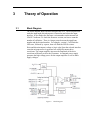
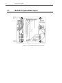
Block Diagram
The block diagram shows the basic design of the 8712. The microprocessor
reads the input mode bits when power is turned on and selects the input
interface. It also flashes the firmware version number on the internal red
LFAULT indicator. To check the firmware version, one has to count the
number of led flashes. There is a longer pause between the significant
number and the decimal number. For example, version 1.5 will flash the
LED once, followed by a pause, then will flash the LED five times.
Pulse and direction inputs (voltage or logic edge) from the selected interface
cause the microprocessor to generate low voltage Picomotor drive
waveforms. The output amplifier increases the amplitude of the drive
waveform sufficiently to drive the Picomotor. An internal power supply
generates the high voltage power for the output amplifier as well as other
supply voltages.
Figure 9
Block Diagram
10
Theory of Operation
When LIDLE is pulled low, the microprocessor shuts down the power supply
and stops generating Picomotor drive pulses. The response to this input is
rapid enough to prevent the generation of more than one pico pulse after
LIDLE goes low. Normal operation resumes after LIDLE is brought high.
3.2
Input Mode Control Bits
MODE0 and MODE1 are decoded when the power is applied. The interface
mode can only be changed by removing power to the 8712, then changing the
mode bits and applying power again. MODE0 and MODE1 define the control
interface as follows:
MODE0
3.2.1
MODE1
Description
0
0
Step/Direction Mode
1
0
Quadrature Mode
0
1
Line Voltage Input
1
1
Bang-Bang Voltage Input
Step/Direction Mode
In this mode, DIR+/A is the direction input. PULSE+/B is the pulse
command input. TTL inputs to the control interface determine pulse
generation and the direction of motion. One Picomotor pulse is generated for
each falling edge of PULSE+/B. PULSE+/B can be left in either a high or
low state because it is edge sensitive. The low state is preferred because the
opto-coupler input diode will be off.
DIR+/A causes clockwise motion when high, and counter-clockwise motion
when low. It is checked before each pulse is made to allow instantaneous
direction reversal. DIR+/A is level sensitive, so it must be in the desired state
when PULSE+/B goes low and remain in that state for a minimum of 100 μs
after PULSE+/B goes low. The pulse rate can be between 0 and 2 kHz. Faster
pulse rates will not result in increased response.
3.2.2
Quadrature Mode
In this mode, DIR+/A is the A-phase input and the PULSE+/B is the B-phase
input. Like the step/direction mode, quadrature mode uses the digital control
interface. In this mode a pulse is generated for every edge transition of both
the A-phase and B-phase control inputs. The direction of motion is
determined by the phase of A with respect to B:
Theory of Operation
11
Figure 10
Quadrature-Mode Operation
In normal operation, the drive pulse rate is 4 times the frequency of the Aphase and B-phase waveforms. Do not exceed the A/B-phase frequency of
500 Hz. The Picomotor drive pulse rate cannot go over 2kHz. A perfect
quadrature phase relationship between A-phase and B-phase will generate
evenly spaced Picomotor drive pulses.
The firmware direction-decoding scheme used in the 8712 rejects edge
chatter on the A and B phase inputs. After the 8712 detects an edge transition
on A or B phase, subsequent edges are ignored until an edge transition is
detected on the other phase.
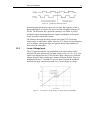
3.2.3
Linear Voltage Input
The 8712 generates a pulse rate proportional to the input voltage on the
ANALOG IN pins in this mode. An input voltage from +10 V to –10 V gives
a pulse rate ranging from 0 to 2 kHz. Positive input voltages give clockwise
motion. Negative input voltages give counter-clockwise motion. There is a
deadband of about ±1 V around 0 V to reject noise. Beyond the deadband
threshold, the pulse rate increases with every 78-mV change in voltage:
Figure 11
Pulse Rate vs. Input Voltage for Linear Voltage Input Mode
12
Theory of Operation
Figure 12
Detailed View of Pulse Rate vs. Input Voltage around the dead-band for
Linear Voltage Input Mode
Voltages between 78-mV steps will cause the pulse frequency to switch back
and forth between two pulse frequencies. Connect ANALOG IN+ to a low
impedance voltage source. Connect ANALOG IN- to the analog signal
ground associated with the source of ANALOG IN+. Ground loop noise can
be introduced into the analog inputs when SYSTEM GROUND is used
instead of analog signal ground. Reverse the ANALOG IN connections to
change the polarity sense of the analog input voltage.
3.2.4
Bang-Bang Voltage Input
In this analog input mode, a voltage exceeding the deadband threshold gives
the maximum 2 kHz pulse rate. Positive input voltages give clockwise
motion. Negative input voltages give counterclockwise motion. This mode
should not be used continuously without forced air cooling of the 8712 at
ambient temperatures higher than 25 °C. The unit has a temperature time
constant of 6 minutes. Operation in Bang-Bang mode is acceptable for less
than 50% duty cycle and less than 3 minutes of continuous operation in still
air at 55 °C.
For heatsink mounting and recommended parts refer to section 3.4.1 and
Figure 14.
3.3
Status Indicators
The red and green LED indicators are visible inside the module’s casing
through small holes. They provide a visual indication of the unit’s status.
Theory of Operation
13
Green and
red LEDs
can be seen
through
these holes.
Figure 13
Status Indicators position
The red LED is tied to LFAULT (pin 15). It will flash the firmware revision
number when the unit is turning on, and will also turn on if the output
amplifier temperature approaches the design limit.(You can also monitor the
temperature using the TEMP MONITOR, pin 21. This pin has a 100 kΩ
output impedance. The relationship between TEMP MON voltage and
output-amplifier temperature is shown in Figure 4.)
The green LED monitors drive pulses. The LED is turned off each time a
Picomotor drive pulse is generated. As the pulse frequency is increased, the
LED is off a greater fraction of time. This dimming effect is used to visually
ensure correct operation.
3.4
Power Supply
The 8712 module can place tremendous stress on the system power supply.
The stress has two components:
3.4.1
Inrush current: The inrush current on power-up charges the internal
filter capacitor. While the energy magnitude of the inrush current is
limited, it can still cause problems with power supplies not designed to
handle it.
Dynamic load: Dynamic current is supplied to the 8712 internal power
supply for each Picomotor drive pulse. The input-filter capacitor will
supply more dynamic current as the resistance between the capacitor and
system power supply increases. Do not increase this resistance: it will
increase ripple-current stress on the internal input-filter capacitor,
leading to early failure of the 8712 module. The best strategy is to keep
the resistance between the power supply and the 8712 below 0.1 Ω and
specify a system power supply that can handle the dynamic current
requirement.
Fault Protection
The 8712 incorporates circuit-protection schemes to protect itself and the
system power supply:
14
Theory of Operation
Over-voltage protection: If the power input voltage exceeds 16.7 to 18.5 V,
a transient voltage suppressor (TVS) shunts the power input to ground. The
internal 2-A fuse will then open. The TVS will also shunt the power input
to ground if an internal fault shorts any high voltage to the power input.
The input fuse will also open if the input power voltage is reversed. Brief
power supply transients will not blow the fuse.
Inrush resistor: A 5.6 Ω resistor handles all input current until the power
supply is operating. This resistor will over-heat and open if an internal
fault occurs before the power supply starts operating.
Over-temperature protection: If the case temperature reaches 80 °C (4 V at
temperature monitor pin 21), the unit will pull LFAULT low to tell the user
that the case, which acts as a heatsink, reached the maximum allowed
temperature. The user is expected to take some measures like decreasing the
pulse rate, air force cool the 8712 case, or use a heatsink. If the case
temperature continues to rise, at 85 °C (4.12 V at temperature monitor) the
output will be turned off. The output will remain off until the case
temperature will decrease to 75 °C (3.86 V at temperature monitor), when the
output will be turned on automatically. If left unattended, the unit will
protect itself cycling between 85 °C and 75 °C.
If a heatsink is needed, 8712 has 4 threaded holes on top (see Figure 14) to
accommodate a standard half brick heatsink. Examples of heatsinks are
Wakefield 528-24AB and 517-95AB. When Wakefield 528-24AB is
mounted on 8712 the unit temperature time constant becomes 10 minutes.
For 517-95AB heatsink the unit temperature time constant becomes 16
minutes.
Heatsink
mounting
holes
Figure 14
3.4.2
Heatsink mounting holes
Power Connections
Special emphasis on proper power-trace routing is needed due to the high
static and dynamic currents demanded by the 8712. Ideally the 8712 will be
placed physically close to its power source. The optically isolated control
interface makes it possible to place 8712 close to the power supply without
Theory of Operation
15
concern for ground loops associated with the control wiring. +V IN and SYS
GROUND should be routed one on top of the other (and with at least 0.5"wide traces).
You can use ground/power planes to route +V IN and SYS GROUND. Use
ground/power planes with caution: continuous planes can allow coupling
between the 8712 power and neighboring circuits. Power planes with
strategically placed slits to control current flow work best. +VIN and SYS
GROUND must not cross any plane slits in their paths to the power source.
The 8712 frame is connected to the internal ground. This connection is made
to improve shielding and reduce leakage currents in the 8712 frame. The four
mounting screws which are connected to the 8712 case should not be
connected to anything on the customer’s printed circuit board.
No additional filter capacitors are needed between +V IN and SYSTEM
GROUND. A common-mode inductor can be used to reduce the effect of
switching power-supply noise and dynamic current.
3.5
Control Interface
This section describes the hardware aspects of the control interface:
MODE1, MODE0. These inputs are not optically isolated and should be
connected to SYSTEM GROUND or +5V OUT at the 8712 connector.
MODE1,0 should be optically isolated if you want to control these inputs
from the host computer. Include the 1 kΩ resistor connected in series to
the +5V OUT pin in any opto-coupler design calculations.
LIDLE, PULSE+/B, DIR+/A. These inputs are optically coupled. They
can be directly driven by an HC-TTL buffer like the 74HC244. A 0.06
W 470 Ω resistor is connected in series with the opto-coupler input diode
to limit current. With 5V input, this resistor only dissipates 0.03 W.
Clearly a higher control voltage could be used to drive the optically
coupled inputs. Calculate the current limiting resistor power dissipation
and add an external resistor if higher drive voltage is used. 3Volt logic
levels are marginal and not recommended for driving the 8712 optically
coupled inputs. When using LIDLE as control signal to activate the
output pulses, depending on power supply inrush current limit, the
typical value of delay time will be typically 400 ms.
LFAULT is an optically isolated output. It presents an open transistor to
the outside world. When on, LFAULT will sink 2.5 mA with 0.2 V
collector-emitter voltage. A 10 kΩ pull-up resistor connected to a +5 V
logic power supply (not +5VOUT) at the termination of LFAULT will
preserve the isolation of this output.
DGROUND is the return signal for all the optically coupled signals
mentioned above. It must be tied to digital ground at the source of
LIDLE, PULSE+/B, DIR+/A and the termination of LFAULT. Do not
16
Theory of Operation
connect DGROUND to SYSTEM GROUND at the 8712 unless you are
just trying to make a simple hook-up to test operation of the 8712.
3.6
Output Connections
PULSE OUTPUT and PULSE RETURN connect the 8712 to the external
Picomotor connector. These signals carry a peak current of 2 A with 15-μs
rise-time and should be routed with care. Route one on top of the other with
minimum 0.15" trace width. Do not route any traces parallel to PULSE
OUTPUT or PULSE RETURN without at least 0.2" of clearance.
Ground/power planes covering these traces can provide excellent shielding at
the risk of increased coupling of the pulse output to the shielding planes.
The 8712 incorporates current-limiting resistors to protect the customer’s
system from serious damage. If the PULSE OUTPUT is shorted, the resistors
will over-heat and open.
3.7
Sockets
The 8712 can be connected to your printed circuit board with female header
sockets:
Make
Model
Digi-Key #
3M
80620078958
929850-01-36-ND
Mill-Max
801-036-10-012000
ED7636-ND
Mill-Max
801-93-050-10-0001
ED7150-ND
These headers come in standard lengths of 36 or 72 pins and can be cut as
needed for the 8712.
The New Focus Picomotor usually comes with a high reliability RJ-11 plug.
The mating receptacle for printed circuit board mounting is available from
many sources:
3.8
Make
Model
Digi-Key #
Hirose (side entry)
TM5RJ3-44
H9081-ND
EMC Considerations
The 8712 was designed for use as a component of a larger system, and
incorporates several design features to improve the overall system’s EMC
performance:
Theory of Operation
17
Output filter: Both PULSE OUTPUT and PULSE RETURN incorporate
inductor capacitor T-networks. The T-networks largely attenuate both
ESD pulses entering the 8712 and microprocessor clock harmonics
leaving the 8712. The bottom of the T-network connects to the 8712
ground.
Frame ground connection: Several pins connect frame ground to the
internal 8712 ground via a 0.1-μF capacitor. This connection is close to
that of the output T-filters mentioned above. Microprocessor clock
harmonics are shunted back to internal ground by the T-network. ESD
energy is shunted to frame ground when the FRAME GROUND pins are
connected to the customers frame ground. This connection must be low
inductance (i.e. short and wide).
Optically coupled control interface: As mentioned above, optical
coupling is used to break the low frequency ground loop inherent in
locating the 8712 close to its power source. Further benefits in the EMC
aspect of system design are the reduction in I/O coupling to the more
sensitive control section of most systems, and the reduction of controller
clock harmonics coupling to the 8712 output.
Additional protection may be needed to provide acceptable EMC
performance of a system incorporating the 8712. An additional set of output
T-filter networks close to the Picomotor connector and equipment bulkhead
will shunt ESD energy before it enters the system. A common-mode powerline filter will reduce radiation/conduction of switching-power-supply
harmonics.
Attention to printed circuit board layout details, as mentioned in previous
sections, will go a long way to ensuring success at the EMC test lab.
4
MODEL 8703 SYSTEM
4.1
Model 8703 System Hook Up
The Model 8703 incorporates the Model 8712 Picomotor Driver Module with
a printed-circuit board for quick and easy hook up into your system. The
board includes connectors and an on-board on-off switch to reset power
whenever necessary. There are four I/O connectors on the Model 8703
system board: J100, J101, J102, and J103. J100 is for the power supply and
J101 is for controlling and monitoring the Model 8703. J102 and J103 are for
pulse output to drive the Picomotor. The terminal functions for J100 and J101
are described below.
4.1.1
I/O Connector Descriptions
Name
J100
J101
J102
J103
Description
2-Pin Header
9-Pin Header
4-Pin
receptacle
3-Position
terminal
Make
Phoenix
Contact
Phoenix
Contact
Hirose
Phoenix
Contact
Model#
MSTBA 2,5/2G-5,08
MSTBA 2,5/9G-5,08
TM5RJ3-44
MKDSN 1,5/3
Digi-Key #
277-1106-ND
277-1113-ND
H9081-ND
277-1237-ND
Model 8703 System
4.1.2
I/O Connector Terminal Functions (Connectors J100 & J101)
Connector
Terminal
J100
Name
Description
1
GROUND
Power return
2
12 VOLTS
Input power, 10–12 V
J101
Voltage-controlled rate input. Connect to analog common.
1
ANALOG IN–
Note: This is connected to the ANALOG IN- of the 8712
module.
2
ANALOG IN+
Voltage-controlled rate input. Connecting to analog
voltage ±10 V gives full-scale rate of 2 kHz. The input
impedance is 14.1 kΩ to ground. Note: This is connected
to the ANALOG IN+ of the 8712 module.
3
OPTO RET
Opto-coupler return. Connect to digital ground close to
control logic.
4
DIR/A
Opto-coupled TTL control input defined by MODE 0,1
inputs. In Step/Direction mode, controls direction:
high=clockwise, low=counterclockwise. In Quadrature
mode, acts as quadrature A.
5
PULSE/B
Opto-coupled TTL control input defined by MODE0,1
inputs. In Step/Direction mode, each falling edge initiates
a step. In Quadrature mode, acts as quadrature B.
6
LIDLE
Opto-coupled TTL input. Low input disables pulse
generation and reduces power consumption. Can also be
used as system interlock.
LFAULT
Open-collector opto-coupler output pulled low when
output amplifier temperature limit is exceeded. On startup, firmware version number is present on this pin in the
form of on/off pulses.
8
TEMP+
Voltage proportional to the output-amplifier case
temperature. A voltage greater than 4 V (at 80 ºC) pulls
LFAULT low. A voltage greater than 4.12 V (at 85 ºC)
turns the output off. The output is turned on if the voltage
decreases to 3.86 V (at 75 ºC).
9
TEMP
RETURN
Ground reference for terminal 11. Do not tie to GROUND
(terminal 1).
7
4.1.3
19
Setting the Control Mode
Set the Model 8703 control mode using the DIP switches located at S100.
These switches control the MODE0 and MODE1 driver inputs.
20
Model 8703 System
4.1.4
Power Input
Supply power to the Model 8703 via the 2-pin connector, J100. Connect Pin
1 to the power source ground, and connect Pin 2 to the +10 V to +12 V power
source. Diode D107 and D108 protect the Model 8703 against reversed
power wiring.
4.1.5
Analog Control
Connector J101 provides interface for control and monitor signals. Pins 1 and
2 are inputs for the analog voltage used to set the pulse rate. These inputs are
only used when the DIP switches at S100 are set for LINEAR (off on) or
BANG-BANG (off off). Connect ANALOG IN+ to a positive voltage and
connect ANALOG IN- to the analog ground associated with the ANALOG
IN+ voltage source: reverse the polarity to change the direction of the
Picomotor. D100 and D101 are bipolar TVS diodes that shunt voltage spikes
to GROUND. D100 and D101 are most useful when long wires are used to
connect Pins 1 and 2 to the pulse-rate-controlling voltage source.
4.1.6
Digital Control
Pin 3 is the return line for the DIR/A, PULSE/B, LIDLE, and LFAULT optoisolators. Connect it to the logic ground for the source of these signals
(destination for LFAULT). Pin 3 can be connected to terminal 1 GROUND if
a simple set-up is needed. DIR/A, PULSE/B, LIDLE, and LFAULT will
function only if terminal 6 is connected to the proper ground.
Pins 4 and 5 are used for step and direction input when the DIP switches are
set for DIR/PULSE (on on) or QUAD (on off). See the data sheet for a
detailed discussion of the digital control modes. R100 and R101 limit the
current flow through the opto-isolator inputs. If 5V logic (TTL) drives Pins 4
and 5, the current-limiting resistors in the Model 8703 are sufficient. R100
and R101 should be increased if higher voltage logic is used. For example,
suppose you want to use 12V logic:
The 8712’s internal 470 Ω 0603-package resistor’s maximum
dissipation=0.063 W.
The opto-isolator diode drop=1.4 V.
You should calculate R such that the internal resistor dissipation is 50% of
maximum, at 0.032W.
0.032 W
8.2mA
470
12V 1.4V 470 8.2mA
822
R
8.2mA
Rounding to the nearest 10% standard resistor value results in a value of
R=820 Ω.
Current I
820 Ω x (8.2 mA2) = 0.055 W, so the 0603 package is marginal and you
should use 0805.
Model 8703 System
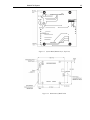
Figure 15
4.1.7
21
Schematic of Model 8703 System Board
LIDLE
Pin 6, LIDLE, is connected to the positive logic voltage to enable 8712
operation and left floating or grounded to disable the 8712. The 8703 will not
operate if Pin 6 is grounded or floating. Opto-isolator U100, Q100, R107-9
light diode D109 to indicate when Pin 6 is grounded or floating while
preserving the isolation barrier. R102 serves the same purpose as R100 and
R101. The same calculations apply for determining the value of R102. You
can just connect an 820Ω resistor between the 12V supply and Pin 6 to
disable LIDLE.
4.1.8
LFAULT
Pin 7 is the open collector opto-isolated LFAULT output. It goes low when
the case temperature limit is exceeded. LFAULT pulses when power is first
applied to indicate the firmware revision number. The data sheet gives an
example of the pulsed startup waveform. The customer must provide a pullup resistor on the LFAULT output. The pull-up resistor is connected to the
logic power supply near the destination of the LFAULT signal.
An example calculation of the pull-up resistor value is given below:
Opto-isolator diode current = 7 mA
Vce saturated = 0.3 V with Ic = 4 mA when the diode current = 7 mA
With 5V logic,
22
Model 8703 System
5V 0.3V
1.18k
4mA
Rounding to the nearest 10% value, 1.2 kΩ,
R
1.2k (4mA) 2 0.019W
Therefore the 0603 package is can be used in this application.
For 12V logic,
12V 0.2V
2.9k
4mA
Rounding to the nearest 10% value, R=2.7 kΩ,
R
2.7 k (4mA) 2 0.043W
So the 0603 package is marginal and you should use 0805.
4.1.9
Temperature Sensor
Pin 8 is connected to the 8712 temperature sensor output. The output
impedance is 100 kΩ, so use a high impedance input to monitor this terminal.
See Figure 4 for a typical voltage vs. temperature plot. The thermistor used in
the 8712 temperature sensing circuit has a ±10% tolerance. C100 is
connected across Pins 8 and 9 to improve noise filtering. TVS diode D106 is
connected across Pins 8 and 9 to attenuate voltage spikes. D106 is not needed
if short wires are used to connect Pins 8 and 9 to the input of the voltage
measuring circuit.
Pin 9 is the ground reference for the temperature sensor.
4.2
Picomotor Connections
For the convenience of your application, the Model 8703 system board
provides two connectors, J102 and J103, to connect the 8703 Drive Module
to the Picomotor.
J103 has 3 screw terminals for connection to the Picomotor wires and an
optional cable shield.
Terminal
Name
Description
1
FRAME GROUND
Return for EMI T-filter on PULSE
RETURN and PULSE OUTPUT.
2
PULSE OUTPUT
Drive pulse.
3
PULSE RETURN
Drive pulse return.
Model 8703 System
23
CAUTION
The Picomotor will be damaged if the PULSE RETURN and
PULSE OUT connections are reversed. Check with New Focus if
you have any questions about Picomotor wiring when using
J103.
Also, be careful when connecting a scope probe to the unit
output. The probe clip is connected to the scope chassis
ground. If the probe clip is accidentally connected to the 8712
Pulse Output, the output stage may be damaged.
4.2.1
Isolation
The system board includes some circuitry to isolate the 8712 from the
Picomotor cabling. L102 and L101 ferrite beads increase the impedance to a
few hundred Ohms at high frequencies. D111 and D110 TVS diodes shunt
high voltage pulses to the frame ground terminal PX600. The frame ground is
also connected to the 8712 to ground the internal filter-T networks.
The pulse output, pulse return, and frame traces are low inductance. Pulse
output and return carry 2 A transient currents and must be tightly coupled.
The frame connection is also low inductance; it carries high current with
wide bandwidth when ESD events occur. The connection to system frame
ground is made with screw terminal PX600. Use a short wire or metal
binding post to connect PX600 to the equipment frame.
24
Model 8703 System
4.3
Model 8703 System Board Layout
Figure 16
System Board (Upper Layer, Top View)
Model 8703 System
25
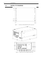
Figure 17
System Board (Bottom Layer, Top View)
Figure 18
Dimensions of Model 8703.
5
Safety Precautions
5.1
Definitions and Symbols
The following terms and symbols are used in this documentation and also
appear on the Models 8712 and 8703 where safety-related issues occur.
5.1.1
General Warning or Caution
Figure 19
General Warning or Caution Symbol
The Exclamation Symbol in the figure above appears on the product and in
Warning and Caution tables throughout this document. This symbol
designates that documentation needs to be consulted to determine the nature
of a potential hazard, and any actions that have to be taken.
5.1.2
Electric Shock
Figure 20
Electrical Shock Symbol
The Electrical Shock Symbol in the figure above appears throughout this
manual. This symbol indicates a hazard arising from dangerous voltage.
Any mishandling could result in irreparable damage to the equipment, and
personal injury or death.
5.1.3
European Union CE Mark
Figure 21
CE Mark
The presence of the CE Mark on Newport Corporation equipment means that
this instrument has been designed, tested and certified compliant to all
applicable European Union (CE) regulations and recommendations.
Safety Precautions
5.1.4
27
Waste Electrical and Electronic Equipment (WEEE)
Figure 22
WEEE Directive Symbol
This symbol on the product or on its packaging indicates that this product
must not be disposed with regular waste. Instead, it is the user responsibility
to dispose of waste equipment according to the local laws. The separate
collection and recycling of the waste equipment at the time of disposal will
help to conserve natural resources and ensure that it is recycled in a manner
that protects human health and the environment. For information about
where the user can drop off the waste equipment for recycling, please contact
your local Newport Corporation representative.
5.1.5
Control of Hazardous Substances
Figure 23
RoHS Compliant Symbol
This label indicates the products comply with the EU Directive 2002/95/EC
that restricts the content of six hazardous chemicals.
5.2
Warnings and Cautions
The following are definitions of the Warnings, Cautions and Notes that are
used throughout this manual to call your attention to important information
regarding your safety, the safety and preservation of your equipment or an
important tip.
WARNING
Situation has the potential to cause bodily harm or death.
CAUTION
Situation has the potential to cause damage to property or
equipment.
28
Safety Precautions
NOTE
Additional information the user or operator should consider.
5.2.1
General Warnings
Observe these general warnings when operating or servicing this equipment:
Heed all warnings on the unit and in the operating instructions.
Do not use this equipment in or near water.
Although the input power to this equipment is below 20 VDC, this
5.2.2
equipment internally generates much higher voltages that are present on
the Model 8712 connector pins AND various components and connectors
on the Model 8703 System Board. Only properly trained personnel
should touch either of these items.
The Model 8712 is intended to be used as a component in a larger
system. When this product is included as part of a larger assembly, the
user MUST ensure that appropriate additional safety and EMCcompliance features are incorporated the assembly.
The Models 8712 and 8703 are powered from an external DC source that
is not part of either product. When the external power source is
connected to MAINS power, the user must ensure that an appropriate
disconnect switch and fuse are incorporated into the external power
source.
Disconnect power before cleaning the equipment. Do not use liquid or
aerosol cleaners; use only a damp lint-free cloth.
Lockout all electrical power sources before servicing the equipment.
There are no user-replaceable fuses in this equipment. The user must
ensure that appropriate current-limiting protection is provided by the
external DC power source.
To avoid explosion, do not operate this equipment in an explosive
atmosphere.
Qualified service personnel should perform safety checks after any
service.
General Cautions
Observe these cautions when operating this equipment:
If this equipment is used in a manner not specified in this manual, the
protection provided by this equipment may be impaired.
Do not block ventilation openings.
Use only the specified replacement parts.
Follow precautions for static sensitive devices when handling this
equipment.
Safety Precautions
29
This product should only be powered as described in the manual.
There are no user-serviceable parts inside the Model 8712 Picomotor
Drive Module.
5.2.3
Summary of Warnings and Cautions
The following general warning and cautions are applicable to this instrument:
WARNING
The Picomotor Driver is incomplete in constructional features
and is considered only to be a component for the purposes of
regulatory compliance. It is “equipment for building in;” a
suitable enclosure must be provided so that the unit is not user
accessible when incorporated into the final product.
WARNING
The Model 8712 Picomotor Driver internally generates non-SELV
voltages and shall be installed with the enclosure, mounting,
spacings, and marking requirements of the end-use application.
WARNING
The Model 8703 Picomotor Driver kit has exposed non-SELV
voltages that may exceed 130 volts. This unit is only for use by
trained, experienced personnel. The unit should not be powered
when untrained personnel can access it.
WARNING
Do not attempt to operate this equipment if there is evidence of
shipping damage or you suspect the unit is damaged. Damaged
equipment may present additional hazards to you. Contact
Newport technical support for advice before attempting to plug
in and operate damaged equipment.
WARNING
Before operating the Model 8712 Picomotor Driver, please read
and understand all of Section 5.
30
Safety Precautions
WARNING
Do not attempt to operate this equipment if there is evidence of
shipping damage or you suspect the unit is damaged. Damaged
equipment may present additional hazards to you. Contact
Newport technical support for advice before attempting to plug
in and operate damaged equipment.
WARNING
Do not apply external DC power to this equipment in excess of
16 VDC.
CAUTION
There are no user serviceable parts inside the Model 8712
Picomotor Driver. Work performed by persons not authorized by
Newport Corporation will void the warranty.
WARNING
If this equipment is used in a manner not specified in this
manual, the protection provided by this equipment may be
impaired.
WARNING
This instrument is intended for use by qualified personnel who
recognize thermal, shock, or laser hazards and are familiar with
safety precautions required to avoid possible injury. Read the
instruction manual thoroughly before using, to become familiar
with the instrument’s operations and capabilities.
CAUTION
The Models 8712 and 8703 Picomotor Driver are designed to be
safe when operated under Normal Environmental Conditions as
defined in EN61010-1:2010. Operation under harsher
environmental conditions can result in severe injury.
Safety Precautions
31
CAUTION
When operated at higher pulse rates for extended periods of
time, the temperature on the outside of the Model 8712’s case
may rise above the “surface temperature limits in normal
operation” as defined in EN61010-1:2010 unless the user takes
appropriate measures. These may include the addition of an
external heat sink, barriers to contact, reducing the pulse
frequency, or other appropriate mitigations. Failure to take
appropriate action when operating the Model 8712 under these
conditions can result in severe injury.
The Models 8712 and 8703 Picomotor Drivers are intended for
use in an industrial laboratory environment. Use of this product
in other environments, such as residential, may result in
electromagnetic compatibility difficulties due to conducted as
well as radiated disturbances.
The Models 8712 and 8703 Picomotor Drivers are designed to
operate in a controlled electromagnetic environment; i.e., where
R.F. transmitters such as mobile telephones may not be used in
close proximity.