1
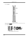
7072 Dual 500ns ADC User Manual copyright FAST ComTec GmbH Grünwalder Weg 28a, D-82041 Oberhaching Germany Version 2.3, May 11, 2009 Copyright Information Copyright Information Copyright 2001-2009 FAST ComTec Communication Technology GmbH, D-82041 Oberhaching, Germany. All rights reserved. This manual contains proprietary information; no part of it may be reproduced by any means without prior written permission of FAST ComTec, Grünwalder Weg 28a, D-82041 Oberhaching, Germany. Tel: ++49 89 6651800, FAX: ++49 89 66518040. The information in this manual describes the hardware and the software as accurately as possible, but is subject to change without notice. ComTec GmbH II Table of Contents Table of Contents 1. Introduction .............................................................................................................................. 1-1 2. Hardware Description .............................................................................................................. 2-1 2.1. Overview ..................................................................................................................... 2-1 2.2. Front panel .................................................................................................................. 2-1 2.2.1. Inputs.............................................................................................................. 2-2 2.2.2. Outputs ........................................................................................................... 2-2 2.2.3. Controls .......................................................................................................... 2-2 2.2.4. Indicators........................................................................................................ 2-3 2.3. Rear panel................................................................................................................... 2-4 2.3.1. ADC port connectors ...................................................................................... 2-4 3. Functional Description ............................................................................................................. 3-1 3.1. Introduction ................................................................................................................. 3-1 3.2. Modes of operation ..................................................................................................... 3-1 3.2.1. Pulse Height Analysis..................................................................................... 3-1 3.2.2. Sampling Voltage Analysis............................................................................. 3-1 3.3. Setting device parameters .......................................................................................... 3-1 3.3.1. Adjust DAC output voltage ............................................................................. 3-2 3.3.2. Adjust ADC threshold ..................................................................................... 3-2 3.3.3. Adjust LLD...................................................................................................... 3-2 3.3.4. Adjust ULD ..................................................................................................... 3-2 3.3.5. Adjust Coincidence / Anti Coincidence .......................................................... 3-2 3.3.6. Normal operation............................................................................................ 3-2 3.3.7. Factory reset .................................................................................................. 3-2 4. Appendix .................................................................................................................................. 4-1 4.1. Specification................................................................................................................ 4-1 4.1.1. Absolute maximum ratings............................................................................. 4-1 4.1.2. Recommended operating conditions.............................................................. 4-1 4.1.3. Power Requirements...................................................................................... 4-1 4.1.4. Connectors ..................................................................................................... 4-1 4.1.5. ADC Signal Timing ......................................................................................... 4-2 4.2. Performance characteristics ....................................................................................... 4-3 4.3. Physical ....................................................................................................................... 4-4 ComTec GmbH III Table of Figures Table of Figures Figure 2.1: Front panel.................................................................................................................. 2-1 Figure 2.2: MONITOR output signals............................................................................................ 2-2 Figure 2.3: Rear panel .................................................................................................................. 2-4 Figure 2.4: ADC port connectors .................................................................................................. 2-4 Figure 4.1: General ADC Signal Timing........................................................................................ 4-2 ComTec GmbH IV Introduction 1. Introduction The Model 7072 is an unique dual channel device that can operate either as an ultra fast pulse height analyzing analog-to-digital converter (PHA ADC) with a fixed conversion time of 500 ns or a sampling voltage analyzer (SVA ADC). The 7072 is ideally suited for high counting rate applications in Energy Spectroscopy. The built-in Single Channel Analyzer (SCA) has a separate output on the front panel. This output can be used in such applications as Moessbauer Spectroscopy. The same connector is used as analog output for monitoring the different threshold levels when they are set in the adjust mode. In the SVA mode a voltage level or wave form can be sampled when a gate signal is applied. The 7072 can be used in any NIM-BIN that supplies +6, +12 and +24 V with 600 mA each. Ample airflow must be provided for sufficient cooling. Do not cover the top or bottom of the NIMBIN. ComTec GmbH 1-1 Hardware Description 2. Hardware Description 2.1. Overview The Model 7072 is a single width NIM module. It has two fully equal and independent channels. Both channels are controlled using the front panel buttons and switches. No jumper or switch inside is necessary. 2.2. Front panel Figure 2.1: Front panel ComTec GmbH 2-1 Hardware Description 2.2.1. Inputs Signal inputs: Two BNC connectors accept +25 mV to +10 V (standard / +8 V optional) positive unipolar (positive lobe leading) pulses, (input impedance = 1 k Ohm, optimized for gaussian shaped pulses with shaping times from 250 ns to 25 µs, dc coupled or a varying voltage level when used in SVA mode. Gate inputs: Two BNC connectors accept positive TTL signals as Gate (input impedance = 10 k Ohm, pull-up in coincidence and pull-down in anti coincidence). Due to the corresponding change from pull-up to pull-down and vice versa PHA analysis does not require any gate input signal connected. 2.2.2. Outputs DAC outputs: Two BNC connectors provide +2.5V variable dc output. Settable in the adjustment mode via the UP/DOWN push buttons. MONITOR outputs: Two BNC connectors. Mode Function Output Operation PHA SCA (Single Channel Analyzer) TTL out SVA Not used DAC output DAC dc output voltage level ADC Threshold ADC threshold level LLD Lower level discriminator level ULD Upper level discriminator level C/A SEL Not used Adjustment Figure 2.2: MONITOR output signals SCA: TTL outputs in PHA mode (TTL pulses of approx. 0.5 µs duration. One output pulse for each input signal that falls between the ULD and LLD thresholds. 2.2.3. Controls Device control is performed using five buttons and two 2-position switches. The 4 main buttons (yellow) on the front panel are used to control the device parameters.These buttons are Up/Down for each of the channels. There is also a Mode button, used to switch between Normal operation mode and different Adjust modes. To prevent accidental changes this button is hidden and accessible with a small screw driver, pencil etc.through a hole in the front panel. Two switches define the functionality of each channel: PHA, SVA. ComTec GmbH 2-2 Hardware Description 2.2.4. Indicators Two 10-LED bars are used as instant deadtime / level indicators. In normal operation mode these LED-bars indicate the deadtime in %. In the different adjust modes the LED-bars provide a raw indication of the currently adjusted parameter in % of the maximum value. There is no sign. The real value can be measured with a voltmeter at the front panel MONITOR output. Two additional sets of LEDs indicate the adjusted parameter (if Adj LED is lit) or currently selected range of operation in normal mode. ComTec GmbH 2-3 Hardware Description 2.3. Rear panel Figure 2.3: Rear panel Data: 13 bit binary data lines and data transfer command lines, 25-pin female D-Sub connector on the rear panel (ref. Figure 2.4). 2.3.1. ADC port connectors Figure 2.4: ADC port connectors ComTec GmbH 2-4 Functional Description 3. Functional Description 3.1. Introduction The 7072 has two different modes of operation: • PHA: Pulse Height Analysis • SVA: Sampling Voltage Analysis Any channel can be set in any mode of operation independently. All settings of each channel are done via push buttons on the front panel. In normal operation the range and conversion gain are set using the corresponding UP/DOWN push buttons of each channel. To change any voltage level or the GATE mode from coincidence to anti-coincidence pressing the MODE button will switch into the adjustment mode indicated by the ADJUST LED lit. Now the corresponding voltage level is changed by the UP/DOWN buttons.Subsequent pressing the MODE button cycles through the different adjustments until you are back to normal operation. 3.2. Modes of operation 3.2.1. Pulse Height Analysis In this mode of operation both channels accept analog input signals between 0.025 and 10 V and measure the peak amplitudes that are higher than LLD and lower than ULD thresholds. Outside of that range there is no conversion. To prevent triggering from noise and to adjust for small input offset voltages an ADC threshold is settable in the range of –781 mV … ULD or +1 V whichever is greater. The default value is +78 mV. PHA is triggered only when the input signal rises over this ADC threshold. A subsequent conversion is enabled only when the signal has been fallen under this threshold again. Thus, pileup rejection is provided. When adjusting the ADC threshold it "pushes" the LLD if reached. Thus, the LLD level is always greater or equal to the ADC threshold. 3.2.2. Sampling Voltage Analysis In this mode of operation the corresponding channel accepts analog input signals between 0 and +10 V and measures the voltage when the GATE signal goes low to high in coincidence and high to low in anti-coincidence. In the SVA mode of operation, if the analog input voltage to the ADC is outside of the normal 0-10 volt range (exact range may vary slightly from unit to unit), the converted digital output will be channel zero if the voltage is greater than the normal range, and channel 8191 if it is below the normal range (firmware version V84 starting Feb 2007). The firmware version and date can be found on a label at the backside of the 7072 board. 3.3. Setting device parameters Pressing the MODE button with a small screw driver, pencil or similar will cycle through the following adjust modes: Adjust DAC output voltage --> Adjust ADC threshold --> Adjust LLD --> Adjust ULD --> Adjust Coincidence / Anti Coincidence --> Normal operation An indication of beeing in the adjustment mode is the AGJUST LED lit. All of the levels are set in steps of 4.88 mV. ComTec GmbH 3-1 Functional Description During adjustment the monitor output corresponds to the real level at the analog input. I.e. if the measured monitor level of ULD is 8 V, the ADC will not convert any input pulse with an amplitude over 8 V. 3.3.1. Adjust DAC output voltage Using the yellow UP/DOWN buttons the DAC output voltage of the corresponding channel is set in the range of -2.5 to +2.5V. 3.3.2. Adjust ADC threshold Using the UP/DOWN buttons the ADC threshold of the corresponding channel is set in the range of -780 mV upto +1 V. If the ADC threshold reaches the LLD threshold the LLD level is “pushed” to keep it equal (not lower!) to the ADC threshold. 3.3.3. Adjust LLD UP/DOWN buttons set the lower level discriminator, continuously adjustable from ADC threshold to ULD threshold. If the LLD threshold reaches the ADC threshold on the way down the ADC threshold is “pushed” down to keep it equal (not higher!) to the LLD threshold. 3.3.4. Adjust ULD UP/DOWN buttons set the upper level discriminator, continuously adjustable from LLD threshold to +10 V. 3.3.5. Adjust Coincidence / Anti Coincidence UP/DOWN buttons set the coincidence/anti-coincidence for ADC and SVA modes. 3.3.6. Normal operation When the device is in normal operation mode the UP/DOWN buttons select the conversion range of the ADC. The conversion range of each channel cycles through 8k - 4k - 2k - 1k - 512 - 256 8k - etc. 3.3.7. Factory reset To reset all device parameters to the default values as the 7072 was shipped from the factory press both DOWN BUTTONS simultanously during power-up. ComTec GmbH 3-2 Appendix - Specification 4. Appendix 4.1. Specification 4.1.1. Absolute maximum ratings Input voltage: any analog signal input: ......................................................... +12 V any other input: ............................................................-0.5 ... +5.5 V DC input current: any analog signal input: ...................................................... +15 mA any other input: .................................................................... +15 mA 4.1.2. Recommended operating conditions Supply voltage: (from NIM-BIN supply) .................... +6 V, -6 V, +12 V, -12 V, +24 V Temperature range: ........................................................................................... 0 to 50 °C PHA mode: Amplitude: .................................................................................. 0.025 … +10 V Pulse form: .............................................................................. Gaussian shaped Signal shaping time: ................................................................................. 250 ns … 25 µs GATE setup time: to peak................................................................................... >32 ns GATE hold time: after peak .............................................................................. >32 ns GATE width: ............................................................................................... >65 ns SVA mode: Amplitude: ......................................................................................... 0 … +10 V GATE width: ............................................................................................... >65 ns GATE to sampling delay: ............................................................................................... <32 ns 4.1.3. Power Requirements Supply current: 4.1.4. .................................................................................... +24 V / 40 mA .................................................................................... +12 V / 20 mA ................................................................................... +6 V / 700 mA .................................................................................... -6 V / 120 mA ................................................................................... -12 V / 150 mA Connectors SIGNAL Input Accepts positive unipolar (positive lobe leading) pulses for PHA, optimized for gaussian shaped pulses with shaping times from 250 ns to 25 µs, dc level or pulses for the SVA mode; amplitude 0 to +10 V, +12 V maximum; Zin =1 k, direct coupled; front panel BNC. ComTec GmbH Appendix 4-1 Appendix - Performance characteristics GATE Input Accepts a positive logic pulse or dc level; high amplitude >+2.5 V, Low amplitude <400 mV, 0 to +6 V maximum; dc coupled; Loading with COINCidence selected is 4.7 k to +5 V and 4.7 k to 0 V for ANTIcoincidence; width >100 ns; PHA analysis does not require a gate input. DAC Output Voltage range: ................................................................................................ +2.5 V Output impedance: ...................................................................................... approx. 50 Ω MONITOR Output ..................................................................................... approx. 50 Ω Output impedance: 4.1.5. ADC Signal Timing General ADC Signal Timing 7072: THRESHOLD ANALOG INPUT DEADTIME COINC GATE SCA /DRDY /DACC DATA VALID TIME TO PEAK CONVERSION TIME DECAY TIME DEADTIME = Time-to-peak + MAX(DecayTime; ConversionTime) Figure 4.1: General ADC Signal Timing ComTec GmbH Appendix 4-2 Appendix - Performance characteristics 4.2. Performance characteristics Range: .................................................... 256, 512, 1024, 2048, 4096, 8192 Conversion time: fixed conversion time ........................................................... 500 ns Countrate capability: ......................................................................... > 1.000.000 events/s ADC deadtime: time-to-peak + 500 ns fixed conversion time + data transfer time of 100 ns to buffer (there could be an additional dead time if the MCA can not accept the data rates generated by the 7072T - this depends on the MCA used) ............................................................. Typical ADC deadtime for fast rising input pulses is less than 2 us per event using FAST ComTec MCAs Resolution: 8k range, 500ns flat top pulses ........................... ≤ 3.4 chs1 FWHM Integral non-linearity: linear fit...................................................... typ. +0.16% @ 8k range linear fit...................................................... typ. +0.16% @ 4k range Differential non-linearity: including effects from integral non-linearity........ for 99% of usable channels ............................... including effects from integral non-linearity........ for 99% of usable channels ............................... Peak shift: upto 700 kcps, SVA mode ................................................. +0.006% upto 1000 kcps, SVA mode.................................................. +0.08% Unused channels: .................................................................... approx. top 1% of range Analog bandwidth: ............................................................................................. 3.3 MHz GATE to sampling delay: SVA mode: ...................................................................... 0 … 32 ns ±1.1% @ 8k range ±0.7% @ 8k range ±0.7% @ 4k range ±0.5% @ 4k range ADC 120000 Counts 100000 80000 60000 40000 20000 0 50 10 0 0 15 0 00 20 0 25 0 0 30 0 00 35 0 40 0 00 45 0 50 0 00 55 0 60 0 00 65 0 70 0 0 75 0 00 80 00 0 Channel Figure 4.2: PHA, typical noise spectrum 1 channels ComTec GmbH Appendix 4-3 Appendix - Physical ADC 2,0% Diff. Lin. (: 3 chs) 1,5% 1,0% 0,5% 0,0% -0,5% -1,0% -1,5% 10 00 15 00 20 00 25 00 30 00 35 00 40 00 45 00 50 00 55 00 60 00 65 00 70 00 75 00 80 00 -2,0% Channel Figure 4.3: ADC, typical differential linearity plot 4.3. Physical Physical size: single width NIM module (1.35 x 8.71 inches; 3.43 x 22.13 cm) as per TID - 20893 (rev.) Shipping weight: ............................................................................. 1.8 kg (net 1.0 kg) ComTec GmbH Appendix 4-4